HAL Id: tel-01343937
https://tel.archives-ouvertes.fr/tel-01343937
Submitted on 11 Jul 2016
HAL is a multi-disciplinary open access archive for the deposit and dissemination of sci-entific research documents, whether they are pub-lished or not. The documents may come from teaching and research institutions in France or abroad, or from public or private research centers.
L’archive ouverte pluridisciplinaire HAL, est destinée au dépôt et à la diffusion de documents scientifiques de niveau recherche, publiés ou non, émanant des établissements d’enseignement et de recherche français ou étrangers, des laboratoires publics ou privés.
cells
Jie Zhang
To cite this version:
Jie Zhang. Roles of the n-type oxide layer in hybrid perovskite solar cells. Chemical Physics [physics.chem-ph]. Université Pierre et Marie Curie - Paris VI, 2015. English. �NNT : 2015PA066634�. �tel-01343937�
Université Pierre et Marie Curie - Paris VI
École doctorale de Chimie Physique et de Chimie Analytique de Paris Centre
(ED 388)
ROLES OF THE n-TYPE OXIDE LAYER IN HYBRID
PEROVSKITE SOLAR CELLS
Présentée par
Jie ZHANG
Pour obtenir le grade de docteur
Soutenance le 22 Octobre 2015
Devant un jury composé de:
Dr. Thierry Pauporté Directeur de Recherche CNRS–
ENSCP – Paris
Directeur de thèse
Pr. Bernard Ratier. Professeur – Université de Limoges Rapporteur
Dr. Samir Farhat Maître de Conférence – Université
Paris XIII – Villetaneuse
Rapporteur
Dr. Zhuoying Chen Chargée de Recherche CNRS– ESPCI
– Paris
Examinateur
Pr. Christel Laberty Professeur – Université P. et M. Curie
– Paris
Examinateur
I dedicate this thesis to my family for their constant support and unconditional love. I love you all dearly.
ACKNOWLEDGEMENTS
It would not have been possible to write this doctoral thesis without the help and support of the kind people around me. Though many individuals aided me, I would like to highlight and thank in particular the following people.
I would like to acknowledge the Guangzhou Government for financing my scholarship (Oversea Study Program of the Guangzhou Elite Project).
I would like to express my deepest appreciation to my thesis director, Dr. Thierry Pauporté, for giving me the chance to work on this interesting topic. I would like to thank him for his guidance and advice during these past three years of research, investigation and his help in writing publications. I am grateful for his patience and endless support while correcting my thesis manuscript. I feel I have developed a stronger understanding of research and scientific writing.
I would like to thank Dr. Odile Majérus, Dr. Bruno Viana, and Patrick Aschehoug for assistance in performing the Raman, the PL measurements and other characterization techniques during these three years.
I would like to thank Pr. Bernard Ratier, and Dr. Samir Farhat for accepting to be my rapporteurs, as well as Dr. Zhuoying Chen and Pr. Christel Laberty for being my examiners.
I am deeply grateful to all my colleagues and friends for their help, their support, for all the great times we shared, and the many scientific discussions. I would like to thank in particular Dr. Yuly Kusumawati, Ricardo D’Angelo, Alexandra Szemjonov, Sana Koussi, Fan Sun, Dr. Mongia Hosni, Ronghua Li, Yanpeng Xue and many others.
Lastly I would like to thank my family for all their love and encouragement. For my parents, who raised me with love and always supported me in all my pursuits.
vii
Abstract
Solar energy is one of the most important resources in our modern life. Photovoltaic is the most important technology to render the solar energy usable since photovoltaic solar cells harvest light coming from sun and convert sunlight into electrical energy.
Dye sensitized solar cells have gained widespread attention due to their low cost, easy fabrication technique and tunable choice for the device. A traditional DSSC device includes a dye-sensitized photo-anode, a counter electrode and an electrolyte containing a redox couple system and additives. To improve the device stability, the liquid electrolyte replacement by a solid state hole transport material has been studied in so-called solid-state dye sensitized solar cells (ssDSSCs). Recently, an amazing light perovskite absorber was introduced into the ssDSSC system to replace the dye, opening the new field of research. Perovskite solar cells (PSCs) open a new era in photovoltaic due to the low cost of this material and the high efficiency of these cells. The power conversion efficiency has risen from 3.8% to a certified 20.1% within a few years.
The components in the perovskite solar cell include: the compact metal oxide blocking layer, the electron transport layer, the lead halide perovskite layer, the hole transport layer and the back contact. In this thesis, we focused on the preparation and improving the properties of the electron transport layer and the perovskite layer.
In Chapter 2, we describe the technique that we have developed in this thesis for the preparation of various ZnO and TiO2 nanostructures. Anatase TiO2 is n-type semiconductor
with a bandgap of 3.2 eV, and ZnO is also a wide bandgap n-type semiconductor with a large bandgap of 3.37 eV at room temperature. Compared to TiO2, ZnO has a higher electronic
mobility which is favorable for the electron transport. High quality and well-covering i-ZnO layers electrochemically deposited from zinc nitrate precursor solution have been developed. In Chapter 4, we describe a fast and low temperature technique to prepare ZnO layer in a zinc nitrate medium. The morphology and thickness of ZnO nanostructure were controlled through changing the deposition time. The ZnO/perovskite CH3NH3PbI3/ HTM
(spiro-OMeTAD)/Ag cells were fabricated at low temperature, and their properties were characterized. An optimized cell efficiency close to 11% has been achieved with ZnO layer prepared using very fast 120 s of ZnO deposition time. Well-conducting ZnO nanostructures
viii
have also been deposited in chloride/oxygen medium, ranging from arrays of NWs/NRs to the dense, well-covering columnar layers. The surface properties of these ZnO NW/NR structures have been improved by the electrodeposition of a very thin i-ZnO conformal overlayer. In Chapter 3, the two-step technique to prepare CH3NH3PbI3 perovskite for ZnO
NWs/NRs is described. The NWs/NRs structures favor the perovskite sensitizer loading and give rise to the higher short circuit current. Moreover, the cell performance of ZnO NWs/NRs with the thin intermediate overlayer of ZnO could be improved and enhanced.
We also prepared TiO2 nanotube array layers and mesoporous TiO2 nanoparticle films.
One-dimensional TiO2 nanotube array layers were synthesized from single-crystalline ZnO
nanowire (NW) arrays. The ZnO NW layer was converted into anatase TiO2 NTs using a
titanate solution adjusted at an ad-hoc pH. The tubes were polycrystalline and their diameter and length could be tuned to get dimension-tailored nanostructures. In Chapter 6, we investigated the effect of the thickness of TiO2 nanotube layers and improved the cell
performance through improvement of the surface of TiO2 NT layer.
CH3NH3PbI3 perovskite is the most important component in the perovskite solar cell. In
Chapter 5, we compare two kinds of techniques for the preparation of the CH3NH3PbI3
perovskite layers. In the "one-step" technique, a solution is used for the deposition of a precursor layer which is dripped and subsequently annealed. In the "two-step" sequential technique, a PbI2 precursor layer is converted into perovskite. We show that on ZnO, the
annealing treatment of the "one-step" deposited layer is optimum for a duration time of only 2 min. This duration is much less critical for the TiO2 underlayer. Long annealing times
produce the degradation of the pigment and formation of PbI2. It is also shown that the
"one-step" technique gives better results for the sensitization of smooth oxide underlayers whereas the "two-step" one must be utilized for rough or structured underlayer sensitization. The best solar cell performances were achieved by combining a low-overvoltage electrodeposited ZnO layer, a planar architecture and a perovskite layer prepared by a "one-step" deposition-dripping route. A maximum overall conversion efficiency of 15% was measured for the ZnO-based perovskite solar cell. Cell impedance spectra have been measured over a large applied voltage range. Their analysis, using an ad-hoc equivalent circuit, shows that charge recombinations are reduced for the "one-step" perovskite and that a better interface with the oxide is produced in that case.
ix
Briefly, several ZnO and TiO2 nanostructures have been developed in this work applied
to perovskite solar cells. We have characterized the properties of these structures and fabricated perovskite solar cells. Some effects of cell performances have been investigated and used to improve the cell efficiency for the future work.
Keywords: ZnO, TiO2, CH3NH3PbI3, perovskite solar cell, electrochemical deposition,
xi
Contents
Abstract ... vii Chapter 1: Context ... 1 1.1 Introduction ... 1 1.1.1 Solar energy ... 11.1.2 Photovoltaic solar cells ... 2
1.2 Dye-Sensitized solar cells ... 4
1.3 Electron transport process in the ssDSSCs ... 7
1.4 Solar cell photovoltaic characteristics ... 8
1.4.1 Standard solar spectral irradiance ... 8
1.4.2 Current-voltage characteristics ... 9
1.4.3 Quantum efficiency measurement ... 12
1.4.4 Impedance Spectroscopy ... 13
1.5 Perovskite sensitized solar cells ... 19
1.5.1 Introduction of perovskite component ... 20
1.5.2 Recent milestones in the halide perovskite solar cell ... 22
1.6 The components in the perovskite solar cell ... 28
1.6.1 The compact metal oxide blocking layer ... 28
1.6.2 The electron transport layer ... 28
1.6.3 The halide perovskite layer ... 29
1.6.4 The hole transport layer ... 30
1.6.5 The back contact ... 32
References ... 33
Chapter 2: Synthesis and morphological properties of oxide contact layers ... 41
2.1 Introduction ... 41
2.2 ZnO layers electrodeposited from nitrate precursor ... 42
2.2.1 Experimental ... 42
2.2.2 Results ... 43
2.3 Electrodeposition of ZnO in the Chloride/Oxygen System ... 45
xii
2.3.2 Results ... 45
2.4 One-dimensional TiO2 nanotube arrays ... 50
2.4.1 Experimental ... 50
2.4.2 Results and discussions ... 51
2.5 Thin mesoporous TiO2 layer ... 52
2.5.1 Experimental ... 52
2.5.2 Results ... 53
2.6 Conclusion ... 53
References ... 54
Chapter 3: Electrochemical design of ZnO structured layers for efficient PSC application ... 58
3.1 Sensitization of ZnO electrodeposited structures by CH3NH3PbI3 perovskite layers .... 58
3.1.1 Experimental ... 59
3.1.2 The characteristics of CH3NH3PbI3 layer ... 60
3.2 Perovskite sensitized solar cells ... 62
3.3 Conclusion ... 66
References ... 66
Chapter 4: A fast and low temperature preparation method of ZnO films for PSC applications ... 77
4.1 Perovskite sensitized solar cells based on i-ZnO ETL ... 77
4.1.1 Effect of the deposition time of i-ZnO layer ... 77
4.1.2 Effect of the transparent conductive oxide (TCO) substrate ... 79
4.2 Conclusion ... 83
References ... 83
Chapter 5: Effect of oxide contact layer on the properties of CH3NH3PbI3 for PSC applications ... 97
5.1 The preparation and properties of oxide contact layer ... 97
5.1.1 Preparation of oxide contact layer ... 98
5.1.2 Oxide layer characterizations ... 98
5.2 Effect of oxide substrate on the perovskite preparation ... 102
5.2.1 Effect of oxide substrate on the one-step perovskite preparation ... 103
5.2.2 Effect of oxide substrate on the two-step perovskite preparation ... 106
xiii
5.3 Effect of ETL and perovskite preparation route on the solar cell performances ... 111
5.3 Conclusion ... 116
References ... 117
Chapter 6: One-dimensional self-standing TiO2 nanotube arrayed layers designed for PSC applications ... 119
6.1 The preparation and properties of TiO2 layers ... 120
6.1.1 The preparation of TiO2 nanotube arrays. ... 120
6.1.2 The properties of TiO2 nanotube arrays. ... 121
6.2 The properties of perosvskite sensitized solar cells ... 125
6.3 Conclusions ... 129
References ... 129
General conclusion and perspectives ... 132
Annexe I: The preparation and properties of CH3NH3I ... 136
Annexe II: The properties of TiO2 NT layers based dye sensitized solar cells ... 138
List of figures ... 141
List of tables ... 147
List of the abbreviations and symbols ... 149
1
Chapter 1: Context
1.1 Introduction
1.1.1 Solar energy
Energy is one of the most important needs in our modern life. The traditional source of energy, coming from fossil fuels, has been identified as the main reason for the environmental damages caused by the global warming, a consequence of the CO2
concentration increase. Moreover, the fossil fuels are not a renewable source of energy and is rapidly exhausting.[1], [2] Green and renewable energies, such as wind, photovoltaics and hydropower, have been considered as important resources in many countries.[3]–[6] The IEA (International Energy Agency) has estimated that renewable energies are expected to contribute to 450 billion kWh per year by 2030, and the electricity coming from photovoltaic will reach 4572TWh (Figure 1.1).[7] Solar energy has many advantages including: low carbon emission, cleanness, long term resources, low cost and so on….
2
1.1.2 Photovoltaic solar cells
Photovoltaic (PV) solar cells harvest light coming from sun and convert sunlight into electrical energy. PV is the most important technology to render usable the solar energy.[9] In order to enhance the device properties, the understanding of the photo-process mechanisms is necessary. In a crystalline semiconductor, without any dopants, the Fermi energy level lies between the valence band and conduction band. When the material is doped
Figure 1.2 The Band pictures of n-type and p-type semiconductors before (a) and after (b) joining resulting in a p-n junction. (c) Schematic of a classical sandwich solar cell composed of
p- and n-type semiconductor under illumination.
with an electron-donor, the material becomes electron rich and the Fermi level moves closer to the conduction band. This material is called n-type semiconductor. Similarly, when the semiconductor is doped by an electron-acceptor, the Fermi level moves closer to the valence band, and the material is called p-type semiconductor. When an n-type semiconductor is contacted with a p-type semiconductor, the excess electron in the n-type material flows into
3
p-type to recombine the excess holes in the p-type material and similarly the holes flow toward the n-type semiconductor until an equilibrium is reached (Figure 1.2a). Then, the atoms of p-type semiconductor, near the p-n junction, become negatively charged, whereas the atoms of n-type semiconductor, near the p-n junction, become positively charged, an electric field is built (Figure 1.2b). In a classical sandwich solar cell illuminated by photons with an energy level higher than the absorber bandgap, electrons of the valence band are excited and prompted to the conduction band. Due to the presence of an electric field, the electrons drift towards the n-type material and the holes drift toward the p-type material. Finally, the electrons will travel through external wire from the n-type to p-type material and generate a current (Figure 1.2c).
Crystalline silicon photovoltaic devices are called “first generation solar cells” and represent the main photovoltaic products on the market. This technology has limitations due to the high cost of starting material which requires a high purity.[10] The thin film solar cells are classified as “second generation solar cells”, this technology is cheaper but less efficient than silicon photovoltaic. Moreover, its development in the commercial market is limited by the rare (indium…) or toxic (cadmium…) elements.[11] The emerging photovoltaic technologies, called “third generation photovoltaic”, offers the possibility of very low cost fabrication. The dye sensitized solar cells (DSSCs) or the organic photovoltaics (OPV) belong to this category. They are based on cheap starting materials, such as organic molecules, ZnO and TiO2.[12]
Figure 1.3 Images of photovoltaic devices: (a) silicon solar cells, (b) thin-film solar cells, (c) dye-sensitized solar cells.
4
1.2 Dye-Sensitized solar cells
Dye-sensitized solar cells have gained widespread attention due to their low cost, easy fabrication technique and tunable choice for the device.[13] A first low cost, high-efficiency dye-sensitized solar cell was reported in 1991 by M. Grätzel group.[14] Until now, a highest efficiency of 13% has been achieved using a porphyrin-sensitizer and a liquid electrolyte.[15] In the Figure 1.4, the chart affirms the DSSCs’ place as the improving solar technology since silicon. Multicrystalline silicon solar cells, for instance, have crawled up the efficiency ladder from 14% to 20% over two decades. In this chart we also observe that the efficiency of perovskite sensitized solar cell (PSC) has reached a power conversion efficiency of 20% within just two years. PSC are solid-state devices derived from the DSSCs in which the dye is replaced by an hybrid organometal halide and the hole transport is ensured by a solid hole transport material.
Figure 1.4 Performance evolution chart of the best certified research cell efficiencies.[16]
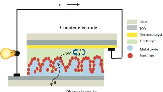
A traditional DSSC device includes a dye-sensitized photo-anode, a counter electrode and an electrolyte containing a redox couple system and additives. The typical DSSC device, architecture is shown in Figure 1.5.
5
Figure 1.5 The device architecture of a typical liquid dye-sensitized solar cell.
Usually, the main active layer is made of a porous, n-type, ZnO or TiO2 semiconductor
film, which is sensitized to the solar light by the adsorption of a monolayer of dye. The oxide receives the electrons photogenerated in the dye and transports the charge carrier from the photo-exited sensitizer to the TCO front contact. The sensitizer is responsible for the light harvesting, and injecting electrons into the oxide conduction band. Then an oxidized sensitizer is produced. This charge separation process is an important step in the solar cell device operation. The other important component in the DSSCs is the electrolyte, which is usually an organic solvent containing a redox system, such as the iodide/triiodide couple or the Co(II/III)tris(bipyridyl), which acts as an efficient electron donor.[17] After the charge separation in the sensitizer, the oxidized sensitizer is regenerated by the electron donor from redox system, and the reduced redox species in the electrolyte is regenerated by an electron provided by the counter electrode.
In the typical DSSC, a liquid electrolyte is used as a redox system. This electrolyte can be replaced by a hole transport material (HTM) contacted by a top metal layer (silver, gold…). The derived device architecture is shown in Figure 1.6. Under light, an electron-hole pair is generated in the sensitizer, the electrons are transported to the TCO contact through the metal oxide, and the holes are transported to the back metal contact through the HTM. The charges can be collected by an external circuit. These devices are called solid-state dye-sensitized solar cells (ssDSSCs).
6
Figure 1.6 The device architecture of a typical solid state dye-sensitized solar cell.
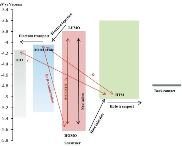
Figure 1.7 Charge generation, transfer and recombination processes occurring in a ssDSSC under illumination.
7
1.3 Electron transport process in the ssDSSCs
This thesis is focused on the solid state perovskite sensitized solar cell, which are derived from the ssDSSCs. Therefore, it is important to understand the electron transfer process in the solid state dye sensitized solar cells. The relevant photo-physical and electron transfer steps are illustrated in Figure 1.7. The basic processes occurring in DSSCs include: photo-excitation, electron and hole injections, electron-hole transports and electron-hole recombination.
Photo-excitation: As mentioned previously, the sensitizer is responsible for the light absorbance and an electron is excited under light from the highest occupied molecular orbital (HOMO) to the lowest unoccupied molecular orbital (LUMO) of sensitizer. When the incident photon energy is higher or equal to the HOMO-LUMO gap energy, the electrons are promoted from a ground state (S) to an excited state (S*).
S S*
Charge carrier injections: after the photo-excitation, the excited sensitizer injects electron into conduction band of the metal oxide semiconductor.[18] After the charge injection process, the sensitizer is regenerated by an electron transfer from the HTM, which is described as a hole transfer from the positively charged sensitizer to the HTM.
S* S+ + e- (electron injection) S+ S+ h+ (hole injection)
Electron-hole transport: subsequent to the electron-hole injection, the electron injected from sensitizer is transported by diffusion to the front contact through the metal oxide layer, and the hole is transported through the HTM and collected at the back contact.
Electron-hole recombination: after charge separation, the electron-hole recombination can also happen. It is a parasitic process that reduces the cell performances. The main recombination pathways occur between electrons in the metal oxide conduction band and holes in the HOMO of the sensitizer (line B), electrons in the TCO and holes in the HTM (line C) and electrons in the metal oxide and holes in the HTM (line D). Another possible loss is when the excited sensitizer goes back to the initial state instead of electron injected into
8
metal oxide (line A). However, the latter phenomenon is avoided by the fast charge injection to the oxide conduction band, this step being much faster than the relaxation one.
In order to reduce the recombination and increase the relative rates of the electron process, the materials selected to fabricate the solar cell are of utmost importance. Many works have been done to improve the charge transport rate and reduce the charge recombination by developing new sensitizers, using different semiconductors, treating the metal oxide surface and so on….
1.4 Solar cell photovoltaic characteristics
1.4.1 Standard solar spectral irradiance
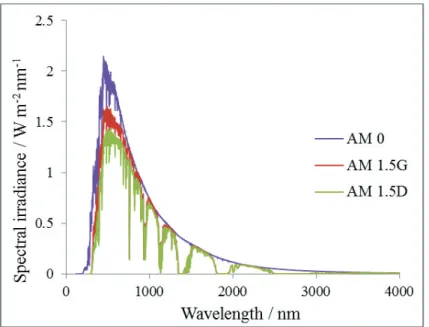
Classical photovoltaic solar cells are electronic devices that use p-n junctions to directly convert sunlight into electrical power. The purpose of the solar cell research is to develop photovoltaic devices that can efficiently convert the energy coming from sun into a usable electrical energy. Because the actual solar spectrum received by a device will vary due to the weather, season, time of day, and location, a standard spectrum has been defined for the determination of the solar cell characteristics and to permit the comparison of devices prepared in various laboratories.
The spectra are standardized by the American Society for Testing and Materials (ASTM). In the Figure 1.8, the solar spectrum used for extraterrestrial application is denoted as Air Mass zero (AM0) based on ASTM standard E 490, and the integrated power of AM0 is 1366.1W m-2. Due to the absorption and scattering when passing through the atmosphere, the solar spectral irradiance is decreased. In the case a solar zenith angle of 48.2°, this solar spectrum is denoted as the AM1.5G (global) standard by ASTM G173, and used for terrestrial applications including direct and diffuse light. The integrated spectral power of the AM1.5G is taken at 1000 W m-2. The AM1.5D spectrum, also based on ASTM G173, is for terrestrial applications but only includes direct light. It integrates to 888 W m-2.[19]
9
Figure 1.8 Reference solar irradiation spectra according to the standards by American Society for Testing and Materials (ASTM).
1.4.2 Current-voltage characteristics
The current-voltage characteristics (J-V curves) are measured in the dark and under illumination, for evaluating the performance of solar cells. This process is done by applying an external potential bias when measuring the current-voltage characteristics. They are measured in the dark and under AM1.5G calibrated illumination. Basically, the forward current, for which the applied potential is referred to as forward bias, involves electrons injection into the cell from the photoanode. The reverse current, for which the applied potential is referred to as reverse bias, involves electrons injection from the counter electrode side.
An ideal dye sensitized solar cells shows a typical diode behavior, the corresponding dark current is shown in the Figure 1.9 (curve 1, red dash line). We found that at low applied potential, very little current (even no current) flow through the device due to the low charge density in the dark. When increasing the applied potential, the charge density increases and the quasi Fermi level is also increased in the metal oxide. When the quasi Fermi level reaches the conduction band of the semiconductor, the electron flow unhindered to the HTM (or liquid electrolyte). So the electrons are injected into the metal oxide and it results in the dark current increase. We can conclude that the dark current is governed by the same electron-hole recombination process as described in the Figure 1.7.
10
Figure 1.9 I-V curve of a typical solar cell under illumination (line) and in the dark (dashed line).
Under illumination, the photocurrent is generated and flows opposite to the diode (dark) current. A typical I-V curve is displayed in the Figure 1.9 (curve 2, red full line). It is governed by two competing processes: the photocurrent generation and electron-hole recombination. At the low potential, most of the charge carriers are collected before they recombine. In that case, the photocurrent does not change with the increasing applied potential. With increasing applied potential, the recombination rate is increased whereas the charge carrier rate is decreased, the photocurrent starts to decrease until without net current flowing to the photoelectrode. When the current is zero, the applied potential point is denoted as the open-circuit potential (Voc). When the external bias is zero, the current is denoted as
the short-circuit photocurrent (Jsc).
The power conversion efficiency (PCE) is the most important parameter for comparing the performance of solar cells. PCE is defined as the ratio of maximum output electrical power (Pmax) to incident power (Pin), as described in the Equation 1.1. The electrical power (P)
is defined as the product of J and V, which is displayed in the Figure 1.9 (curve 3, green line). The maximum of the power curve is called the maximum power point (Pmax), the
corresponding voltage and current are denoted as Jmax and Vmax, described with the Equation
1.2.
PCE=Pmax
11
Pmax=JmaxVmax (1.2)
Another parameter is the fill factor (FF), defined as the ratio between the maximum electrical power (Pmax) to the product of Voc and Jsc. Graphically, the FF also is a measure of
“squareness” of the solar cell characteristic and defined as the ratio of area A to the area B. Finally, the PCE is defined as the Equation 1.4.
FF= Pmax JscVoc= JmaxVmax JscVoc (1.3) PCE=Pmax Pi n = JmaxVmax Pi n = FF JscVoc Pi n (1.4)
The I-V curve of a solar cell can be described by the ideal diode Equation 1.5. In this equation, Jph is the generated photocurrent, Jsat is the saturation current, e is the elementary
charge, k is the Boltzmann constant, T is the temperature and m is an ideality factor (m=1 for an ideal cell).[20] Rs is the series resistance including the contact resistance at interface, the
bulk resistance and the sheet resistance of the transparent electrodes. Rp is the shunt
resistance coming from non-idealities in the p-n junction, recombination at short circuit and presence of electronic defects leading to a leakage current. [21] The equivalent electrical circuit with the resistances Rs and Rp is illustrated in the Figure 1.10.
Figure 1.10 Equivalent circuit of a solar cell.
Considering m, Rs and Rp, the diode equation is modified to Equation 1.6. In the
ssDSSCs, Rs is additionally affected by the transport resistance of the HTM. In contrast to
that, Rp arises from loss processes within the solar cell, leading to a leakage current. In
12
entirely prevent the contact between the TCO and the HTM.
(1.5) (1.6)
1.4.3 Quantum efficiency measurement
In order to determine the ratio of collected charge to the incident photons, the quantum efficiency was introduced. The quantum efficiency can be expressed as the external quantum efficiency (EQE) and internal quantum efficiency (IQE).
The EQE (external quantum efficiency), is also noted as IPCE, for incident photon-to-electron conversion efficiency. This measurement also includes photons which have been lost by optical transmission and reflection. The IPCE is usually measured at the short circuit and can be calculated according to the Equation 1.7, where Jsc is the short circuit current of the
cell under the incident monochromatic light with wavelength (l) and photon flux (J0), and e
is the elementary charge. 0 ( ) ( ) Jsc IPCE eJ l l = (1.7)
The IPCE also can be expressed as the product of the efficiency of four separate physical processes, as shown in the Equation 1.8. Where ηlh is light-harvesting efficiency of
sensitized oxide layer, ηinj is the efficiency of electron injection from the sensitizer into the
oxide, ηcol is the electron collection efficiency, and ηrej is the absorber regeneration
efficiency.[20]
IPCE( )l =h l h l hlh( ) inj( ) col( )l h lrej( ) (1.8)
The internal quantum efficiency (IQE) also referred to as the absorbed photon-to-current conversion efficiency (APCE), corresponds only to the photons absorbed by the device. The equation is:
IQE( )l =h l hinj( ) col( )l h lrej( ) (1.9)
(exp( ) 1) ph sat eV J J J kT = - -( ) (exp( s ) 1) s ph sat p e V JR V JR J J J mkT R + + = - - +
13
A typical quantum efficiency curve is shown in Figure 1.11, for an ideal quantum efficiency, the IPCE would be always 100% for the whole absorbance wavelength resulting as a square shape, but in real solar cells, the quantum efficiency is reduced due to the recombination effects, where the charge carrier are not available to move to the external circuit. The quantum efficiency could be improved by modifying the size of particles, surface of semiconductor and other methods which could affect the charge transport and collection.[22], [23]
Figure 1.11 The typical incident photon to electron conversion efficiency curve.
1.4.4 Impedance Spectroscopy
Impedance spectroscopy (IS) has become a major tool for investigating the properties and quality of solar cell devices. It consists of a measurement of the ac electrical current (I) and a certain ac voltage (V). The electrical resistance (R) is determined from the ratio between the voltage and the current. This is known as Ohm’s law:
R V I
= (1.10) In this law, the resistance is constant. For an ideal conductor, the resistance is zero, and an ideal dielectric (a material that does not conduct electricity) has infinite resistance. In order to
14
extend this concept to alternating current (ac) circuit, the voltage (V) and current (I) need to be treated as time (t), the equations described as:
V( )w =V exp (
[
i w ft+ V)]
(1.11) I( )w = I exp ([
i w ft+ I)]
(1.12) w=2 fp (1.13) where w is angular frequency. For the real conductor, the electrical impedance Z is the complex ratio of the voltage and the current (Equation 1.14) and taken into account both magnitude and phase, j is the phase difference between the voltage and current. For a direct current (dc) circuit, the resistance of the system can be taken as impedance with the same magnitude and zero phase angle.
[
]
[
]
exp ( ) ( ) exp( ) exp ( ) '( ) ''( ) V I V i t Z Z i I i t Z iZw f
w
f
w f
w
w
+ = = -+ = + (1.14)f
V =f f
I+ (1.15) In ac circuit, in addition to the resistance present in the dc circuit, two other impedance phenomena must be considered:(1) The inductance by which voltage are induced in conductor by the magnetic field generated by current.
(2) The capacitance, the electrostatic storage of charge induced by an applied voltage between conductors. Collectively the inductance and the capacitance form the imaginary part of the complex impedance Z” in Equation 1.14, which is referred to as the reactance while the resistance forms the real part Z’.
The capacitance can be determined from the measurement of the change in the electrical charge, which is described by the equation 1.16.
( ) ( ) 1 ( ) ( ) I C i V i Z w w w w w w = = (1.16)
15
Many measure of IS can be described by equivalent circuits composed of combinations of a few elements that are indicated in Table 1.1.
Table 1.1 Relationship and impedance corresponding to bulk electrical elements. Furthermore, the corresponding electrical equivalent circuit symbols are presented. The graphical representation of the impedance is displayed in the Nyquist plots where Z¢ and Z¢¢ are the real
and imaginary components respectively.
Element Relation Impedance Symbol Nyquist
Resistor R V = IR ZR = R Capacitor C I CdV dt = Zc 1 i i C
w
w
C = = -Constant Phase Element Q 1 ( ) 1 CPE n Z i Q Q Zw
= = Inductor L V LdI dt = ZL =i Lw
Equivalent circuits are formed by connecting these elements by wires, representing low resistance paths in the system. When connected in series the current passing through components is the same, while when in parallel they experience the same voltage. The impedance of element in series is additive, and for parallel elements the total impedance is the inverse of the sum of the inverse impedance of the individual components. The impedance for the parallel combination of a resistor and a capacitor is described in Equation1.17. 1 0 1 ( ) ( ) 1 1 1 R R Z i C R i RC i RC w w w wt t w -= + = = + + = = (1.17)
16
An equivalent circuit consisting of the parallel combination of a R and a C element in addition to a simple series resistance R1 is shown in the Figure 1.12a. Figure 1.12b-d display
the perspective of the individual planes. The complex Nyquist plot (Figure 1.12c) of the imaginary impedance component as a function of the real component manifests as an arc, often called RC-arc. The top of the arc occurs at the characteristic frequency w0
corresponding to a relaxation time t (Equation 1.17).
Figure 1.12 (a) Equivalent circuit. (b) Nyquist plot of the spectrum (imaginary as a function of real component). The maximum of the RC-arc takes place at the characteristics angular
frequency w0 as indicated. (c, d) Bode representations of the impedance spectrum: (c)
Magnitude versus the frequency and (d) phase versus the frequency. The simulation was conducted from 1 MHz to 1 mHz.
The high frequency intercept of the arc on the real axis provides a measure of the magnitude of the resistance R1 associated with the system and the low frequency intercept is
equal to R1 + R2. The addition of a series resistance, R1 results in the shift of the RC-arc along
the real axis. Consequently the dc resistance of this system is the sum of the individual resistors, Z(0)= Rdc = R1 + R2, which in this case is 210 W. Hence the data representation in
17
resistances within a system. The frequency dependence of the real and imaginary components presented in Figure 1.12 gives a first indication of the behavior of the magnitude |Z| and phase j of the impedance as a function of the frequency. This is useful in the identification of relaxation processes with different time constants, which therefore manifest at different frequencies.
The definitions discussed above correspond to the ideal cases. To take into account the deviation from ideality, constant phase elements (CPEs) are employed in place of ideal capacitors. The electrical symbol and impedance expression for a CPE are given in the Table
1.1 and Figure 1.13a. A CPE is typically used to describe a capacitive process which is
accompanied by frequency dispersion. The exponent, n accounts for the deviation from the ideal case where n = 1 describes an ideal capacitor while n = 0 corresponds to a pure resistor. In the fitting procedure of IS measurements the CPE exponent is typically fixed or left non-restricted, constraining it between 0.5 and 1. The deviation from ideality manifests in a suppression in the RC-arc in the Nyquist plot as depicted in Figure 1.13b. Furthermore, a decrease in the exponent of the CPE results in slower response times of the capacitor as evident by the shift in the position of the 10000 Hz mark in the Nyquist plot. This is reflected in a decrease in the characteristic frequency with increased deviation from ideality. Where Q is the uncorrected capacitance associated to the CPE (also denoted as CPET) and becomes
equal to the real capacitance when the exponent n (also denoted CPEp) is equal to 1. To determine the correct capacitance C of the system the CPE capacitance needs to be corrected to take into account the associated resistance R:
(
)
1 1 1 1 1 2 n nC
=
é
ê
Q R
-+
R
- -ù
ú
ë
û
(1.18)18
Figure 1.13 (a) Equivalent circuit. (b) Nyquist plot. Bode (c) Magnitude and (d) Phase plot versus the frequency from simulation using the presented values for R1, R2 and CPE. The
exponent of CPE was changed from the ideal case between 1 and 0.5. The red points in the Nyquist plot correspond to the 10000 Hz freqency. The simulation was conducted from 10 MHz
to 1 mHz.
In order to use IS as a tool to examine real system it is necessary to correlate its physical properties with electrical circuit elements. This allows the system to be represented by an equivalent circuit model that can be used to interpret and analyze the IS response of the system. To establish this relationship for solar cells, it is necessary to associate the potentials of the model circuit with the electrochemical potential of the charge carriers in the device.
19
Figure 1.14 Equivalent circuit employed for fitting the impedance spectra.
The simplest IS model of a solar cell consists of a two series combination of CPE//R in series with a high frequency resistance (Rs), as shown in Figure 1.14. Rs is due to the
contacts and FTO layer. In the case of the PSCs, we will see that the high frequency resistance, Rsc is due to the selective contacts and CPE-sc is related to interfacial the
capacitances between the ETM and the HTM and the perovskite. The low frequency loop is assigned to the recombination due to perovskite which gives rise to a resistance noted Rrec
and a CPE-dr which is related to the perovskite dielectric relaxation capacitance. Csc is
determined from Equation 1.18 using Rs as R1 and Rsc as R2. For the determination of Cdr,
(Rs+Rsc) is used as R1 and Rrec as R2.
The recombination resistance needs to be sufficiently large to allow the accumulation of charge carriers in the capacitive element to produce a large solar cell Voc. Selective contacts
are essential to direct the flow of charges and prevent the internal short-circuiting of the device. The low frequency capacitance is a measure of the charge density and is associated with the splitting of the Fermi levels, thus generating a photovoltage.
1.5 Perovskite sensitized solar cells
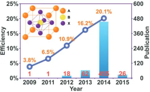
Solar cells employing the perovskite absorber are regarded as a new era in photovoltaic because they combine both a low cost and a high efficiency.[24], [25] Many researches have been focused on the hybrid perovskite solar cells, the power conversion efficiency has risen from 3.8% to 20.1% within a few years [26], [27] as shown in Figure 1.15. In 2009,Tsutomu Miyasaka group reported perovskite’s potential as a light absorber and possible material for a solar cell, noting a 3.8% conversion efficiency.[26] In 2011, Nam-Gyu Park reported a 6.5% efficiency perovskite solar cell.[28] In 2012, several researches have been reported on the
20
improving of perovskite performances. Such as, Michael Grätzel reported a conversion efficiency of exceeding 9% with perovskite in the journal Nature Scientific Reports.[29] Henry J. Snaith reported a “meso-superstructured solar cell” with a power conversion efficiency of 10.9% in a single-junction device under simulated full sunlight. This perovskite solar cell exhibited exceptionally few fundamental energy losses and generated an open-circuit photovoltages of more than 1.1 volts.[30] In the 2013, the efficiency have climbed up to more than 15%.[31], [32] Until now, the highest certified efficiency reached up to 20.1%.[33]
Figure 1.15 Number of publications and efficiency evolution of the perovskite solar cells (updated up to 2015.02.01). The inset is the crystal structure of perovskite (ABX3) with a cubic
symmetry.[34]
1.5.1 Introduction of perovskite component
Historically, the term perovskite has been used to describe the materials with same type of crystal structure as calcium titanium oxide (CaTiO3), which was discovered in 1839 by
Lev Alexeïevitch Perovski.[35]
The chemical formula of the perovskite compounds is AMX3, where A is a large cation
coordinated to 12 X anions and filled in the holes among the octahedral, M is a metal bonded to 6 X anions and X is the anion bonds to A and M. The ideal cubic-symmetry perovskite structure has the M cation in 6 fold coordination, surrounded by the MX6 octahedron anions,
21
1.16). Consequently, only small organic cations, for example those consisting of three or less
C-C or C-N bonds, could be fitted into the structure. Mostly, a slightly perovskite structure distortions can be observed with larger A cation, many physical properties of perovskites, particularly the electronic, magnetic or ferrimagnetism depend on the details of these distortions, which are important for the application of perovskite material.[36]–[38]
Figure 1.16 (a) Ball and stick model (b) three dimensional of cubic perovskite of general formula AMX3.
Halide perovskite (AMX3) is a large perovskite family with X representing halogen
anions (F-, Cl-, Br-, I-). A+ can be a monovalent alkali (Li+, Na+, K+, Rb+, Cs+) or an organic cations (aliphatic amine or aromatic ammonium), M2+ is a divalent metal cation (Cu2+, Fe2+, Pb2+, etc). They form the alkali metal halide perovskite and organo-metal halide perovskite.[39] In 1980, Salau first reported that the direct energy gap of KPbI3 ranges
between 1.4 and 2.2 eV, suggesting its potential used as a solar energy converter.[40]
Distinct from the alkali metal halide perovskite, the organo-metal halide perovskite family has been discovered more recently but has attracted more interest due to its good optoelectronic properties and its potential for application in low temperature device fabrication.[41], [42] The interest about the organo-metal halide perovskite was focused on the photo- and ionic conductivity and semiconducting properties for organic light emitting diodes and thin film transistors applications.[14], [32]
22
1.5.2 Recent milestones in the halide perovskite solar cell
In 2009, Miyasaka first reported the use of organo-lead halide perovskite compounds to efficiently sensitize TiO2 for visible-light conversion in solar cell. The resulting PCEs were
3.81% for CH3NH3PbI3 and 3.31% for the CH3NH3PbBr3.[26]A schematic of the perovskite
sensitized TiO2 and the IPCE action spectra are shown in Figure 1.17. In 2011, N.G. Park
and co-authors fabricated solar cells using TiO2 layer sensitized by about 2-3 nm sized
CH3NH3PbI3 pigment and bumped up the conversion efficiency to 6.54%.[28] However, the
stability of these cells was poor and they were degraded in a few minutes due to the perovskite dissolution in the liquid electrolyte.
Figure 1.17 (a) A schematic illustration of perovskite-sensitized TiO2 undergoing
photoexcitation and electron transfer. (b) IPCE action spectra for photoelectrochemical cells using CH3NH3PbBr3/TiO2 (solid line) and CH3NH3PbI3/TiO2 (dashed line).[26]
In 2012, M. Grätzel and N. G. Park reported the heterojunction solar cell using CH3NH3PbI3 nanoparticles as the light harvesters, and introducing the
2,2’,7,7’-tetrakis-(N,N-di-p-methoxyphenyl-amine)-9,9’-spirobifluorene (spiro-OMeTAD) as a hole transport material to replace the liquid electrolyte. This breakthrough step allowed to boost the power conversion efficiency up to 9.7%, the relative cell device scheme and the I-V curve are shown in Figure 1.18.[29]
23
Figure 1.18 CH3NH3PbI3 perovskite sensitized solar cell device and its photovoltaic
characteristics. (a) Real solid-state device. (b) sectional structure of the device. (c) Cross-sectional SEM image of the device. (d) Photocurrent density as a function of the forward bias
voltage.[29]
In the same year, Henry J. Snaith’s group constructed solar cells where the mesoporous TiO2 was replaced by insulating mesoporous Al2O3 to study their performance. They showed
that the charge transport was faster and the photocurrent unaffected when TiO2 was replaced
by Al2O3. The open-circuit voltage increased to more than 1.1 volts, the power conversion
efficiency increased to the 10.9%. The interesting aspect of this discovery is that the fundamental loss in energy is very low, which gives great promise for significant future increases in efficiency. A schematic illustration of the operating principles of a TiO2-based
perovskite-sensitized and alumina-based meso-superstructured solar cell (MSSC) is shown in
Figure 1.19.[24], [30]
24
Figure 1.19 Schematic illustrating the charge transfer and charge transport in a perovskite-sensitized TiO2 solar cell (left) and a noninjecting Al2O3-based solar cell
(right); a representation of the energy landscape is shown below, with electrons shown as solid circles and holes as open circles.[30]
A year later, M. Grätzel and S. Seok introduce a layered sandwich-type architecture, which comprises a bicontinuous three-dimensional nanocomposite of mesoporous (mp)-TiO2,
with CH3NH3PbI3 perovskite as light harvester, and a polymeric hole conductor, the SEM
image and the schematic of device is shown in Figure 1.20. The use of a polymeric hole conductor improved the performance of solar cells, yielding a power conversion efficiency of 12% under standard AM 1.5 conditions.[31]
Figure 1.20 (a) SEM cross-sectional image of inorganic–organic hybrid heterojunction solar cell. (b) Schematic of device architecture.[31]
25
Before the middle of 2013, the perovskite pigment was deposited using a single step technique by spin coating a mixture solution of PbX2 and CH3NH3X in a common solvent
onto a mesoporous film of TiO2. Due to a wide dispersion of the measured photovoltaic
performance of these devices, J. Bueschka introduced a sequential deposition method to form the perovskite pigment within the porous metal oxide film, and achieve a PCE of 15% with 12% of average efficiency.[32] The cross-sectional SEM of a complete photovoltaic device and J-V curve for a best performance cell is shown in Figure 1.21.
Figure 1.21 The cross-sectional SEM of a complete photovoltaic device (a) and J-V curves for a best performance cell (b).[32]
Usually, a meso-structured semiconductor is used as a selective contact to receive the electrons and transport the negative charge as it is the case in the dye-sensitized solar cells. The holes are collected and transported by the contact with the hole transport material.[14], [43] In the case of DSSCs, the prepared porphyrin sensitized TiO2 mesoporous film solar cell
had a record efficient of 12.3%, whereas the organometal halide perovskite sensitized TiO2
film solar cell also present an efficiency ranging between 10.9% and 16.2%.[23], [24]
After that, H. Snaith and co-authors introduced the simple planar heterojunction (without the complex nanostructures) solar cell incorporating vapor deposited perovskite as the light absorbing layer. They could achieve a solar-to-electrical power conversion efficiency of over 15%.[44] In 2014, Y. Yang group fabricated a perovskite solar cell with high efficiency of about 19.3% through improving the electron transport channel by doping the TiO2 with Yttrium to form the Y-TiO2 ETL, and modifying the ITO with
26
polyethyleneimine ethoxylated (PEIE) to reduce the work function of ITO.[27] The device structure and energy level of each functional layer is shown in the Figure 1.22.
Figure 1.22 Cross-sectional SEM images of the cell device (A), and diagram of energy level of each layer in the device (B).[27]
They also investigated the stability of their perovskite solar cells, when the cell was stored in dry air or nitrogen, the efficiency of device retain 80% of the initial performance in 24h, but only retain 20% of initial efficiency after 6 days of storage in dry air or N2
atmosphere, as shown in Figure 1.23. In that case, stabilizing techniques will be needed for the practical use of these perovskite solar cells.
27
The humidity in the air is an important factor that induces the decomposition of perovskite, and is supposed to explain why the PSC devices are not stable in the ambient air atmosphere. H. Han and co-authors [45] fabricated a perovskite solar cell composed of a double layer of mesoporous TiO2 and ZrO2 as a scaffold infiltrated with perovskite without a
the hole-conducting layer but with a 10-µm-thick carbon layer acting as a water-retaining layer, protecting the perovskite from decomposition in air. This layer also acted as the counter electrode in the device (Figure 1.24 A). The cell achieved a power conversion efficiency of 12.8% and was stable for >1000 hours in ambient air under full sunlight (Figure
1.24 B).
Figure 1.24 (A) Schematic of the triple layer (5-AVA)x(MA)(1-x)PbI3 perovskite based solar cell.
(B) Stability test of a triple layer perovskite sensitized mesoscopic solar cell.[14] B
28
1.6 The components in the perovskite solar cell
1.6.1 The compact metal oxide blocking layer
In order to prevent the direct contact between the TCO and perovskite, a dense metal oxide blocking layer, which fully covers the TCO surface is first deposited on the TCO substrate. Usually, the blocking layer and mesoporous film (electron transport layer) are made of the same material.
Several techniques have been developed to fabricate the metal oxide blocking layer. Aerosol spray pyrolysis and spin-coating are most commonly techniques used.[29], [32] The typical thickness of a blocking layer ranges between 20 and 100 nm, which can be controlled by the concentration of the precursor solution and the spin-coating time.
1.6.2 The electron transport layer
Basically, the metal oxide layer works as a scaffold for the sensitizer and as an electron transport layer for the transfer of the electrons from the sensitized surface to the conductive front substrate. So far, the TiO2 mesoporous layer, which pores are filled with the perovskite
material, yield to a higher PCE, and is the most popular structure for the perovsktie solar cell.[29] TiO2 nanorods[46] and TiO2 nanowire[47], which have the higher electron mobility
in the one dimensional structure compared the TiO2 nanoparticle, have been used to fabricate
a perovskite sensitized solar cell with efficiency of 9.4% and 4.29%. For the other morphology, a TiO2 nanotube,[48] TiO2 nanofiber[49] and TiO2 nanoplatelets[50] have also
been used for the PSSC device.
Compared to TiO2 nanostucture, the ZnO nanostructure is second in popularity. A close
inspection of the perovskite sensitized ZnO show that they can achieve a higher short circuit current, but a lower recombination resistance and a higher recombination rate induces a lower fill factor, which resulted a lower PCE for the ZnO.[51] D. Liu fabricated the CH3NH3PbI3
-based solar cell on ZnO planar nanostructure, and got a conversion efficiency as high as 15.7% on ITO glass and 10.2% on a flexible substrate.[52] Except the TiO2 and ZnO, m-Al2O3 or
ZrO2 and also phenyl-C61-butyric acid methyl ester (PCBM), an organic ETL could work as
29
1.6.3 The halide perovskite layer
Material for the solar light harvesting must have a broad and strong absorbance over the visible to near infrared region of the solar spectrum, this implies a bandgap optimum of 1.4-1.5 eV. This bandgap determines the strength of electrical field which is the voltage. When it is too low, the cell with this semiconductor will collect extra current by absorbing more photons, but having a small voltage. In this case, to balancing these two effects, the optimal band gap for a single junction solar cell is between about 1.4-1.5 eV.[53]
Halide perovskite (AMX3) optical bandgap can be varied by changing the A cation, the
metal cation and the halide cation. The bandgap of perovskite (CH3NH3PbI3 and
CH3NH3PbI3-xClx), usually used in the literature, is 1.58 eV[29] and 1.55 eV[30], respectively.
For the small A cation, such as Cs+, methylammonium (MA+) or formanidinium (FA+), APbI3 prefer to form a three dimensional framework with PbI6 network, and an increase in
the cation size (RCs+ < RMA+ < RFA+) results in a reduction in the band gap, since the values
are 1.73 eV, 1.58 eV and 1.48 eV for the CsPbI3, MAPbI3 and FAPbI3, respectively.
Therefore, a higher efficiency is expected for the FAPbI3 compound compared to
MAPbI3.[53] For the influence of the metal cation, taking the example of AMI3 (M=Sn, Pb),
the band gap of AMSnI3 (1.20 eV) is lower than AMPbI3 (1.58 eV).[54] People have
investigated the influence of the halide anion, the band gap of this group follows the trend AMPbI3 (1.5 eV) < AMPbBr3 (2.2 eV), but the efficiency depends on the ratio of I and Br in
AMPbI3-xBrx.[55]
Compared to the traditional dye solution, the fabrication techniques of the perovskite layers are diverse. The common and simple film deposition methods are one-step precursor solution depositions[56] and the two-step sequential deposition,[32] which two methods have reported the highest efficiency of 19.3% [27] and 15% [32]. The dual-source vapor deposition method permits to prepare an extremely uniform perovskite layer without pin-holes. An efficiency of 15.4% was reported by Liu et al.[44] Y. Yang group reported a low-temperature vapor-assisted solution process to get perovskite film with full surface coverage, small surface roughness and grain size up to the micron scale. The device in a planar architecture with excellent CH3NH3PbI3 film achieved a PCE of 12.1%.[57]
30
1.6.4 The hole transport layer
The hole transport material (HTM) is one of the key components in the solid state solar cells, which is used to transport holes away from the sensitized junction to the back contact of the solar cell. Various materials have been explored as HTM, ranging from low HOMO molecular[58], polymer[31], [59] and inorganic component CuI or CuSCN.[60], [61] In a typical perovskite solar cell, the most commonly used hole transport material is 2,2’,7,7’-tetrakis-N,N-di(4-methoxyphenyl)amine-9,9’-spirobifluorene (spiro-OMeTAD), the molecular structure of spiro-OMeTAD is depicted in the Figure 1.25. Spiro-OMeTAD is an amorphous organic p-type semiconductor with a large bandgap and almost colorless when deposited from solution as a thin film on the substrate. The advantage of spiro-OMeTAD is its good ability to pore filling due to the high solubility in toluene and chlorobenzene organic solvent. Spiro-OMeTAD has a hole mobility in the range of 1 ´ 10-5 to 1 ´ 10-4 cm2 V-1 s-1 as reported in literature.[62]–[65]
Figure 1.25 Molecular structure of 2,2’,7,7’-tetrakis-N,N-di(4-methoxyphenyl)amine-9,9’-spirobifluorene (spiro-MeOTAD), utilized as the HTM in PSCs.
Pristine spiro-OMeTAD has high resistivity and needs to be partially oxidized to decrease the intrinsic charge-transport resistance of the bulk material. This has been achieved through the addition of chemical p-type dopants or through the facile oxidation of the material in the presence of oxygen and light (photodoping).[66]
31
Several additives are added to the spiro-OMeTAD solution to improve its transport properties.[64] The common additives are: 4-tert-butylpyridine (TBP), lithium bis(trifluoromethylsulfonyl)imide (LiTFSI) attributed, or a p-dopant.[32] Usually, the effect of the TBP is believed to be an upward shift of the metal oxide conduction band or a retardation of the electron-hole recombination rate, which leads to an increase in the Voc.[67]–[69] In contrast, the effect of an addition of LiTFSI is a downwards shift of the
metal oxide and accelerate the electron injection. The result is an increase in Jsc.[70], [71]
Furthermore common additives such as Li+ ions have been shown to also contribute to the oxidation and increased hole mobility of spiro-OMeTAD.
Figure 1.26 Time-dependent evolutions of (a) short-circuit current density, Jsc, (b) fill factor, (c)
open-circuit voltage, Voc, and (d) efficiency of the solar cells without encapsulation stored in the
dark and under different atmospheric conditions.[72]
Tom Wu’s group has investigated the effect of different atmospheric storage conditions, particularly vacuum, dry nitrogen, and dry air, on the photovoltaic performance of TiO2/CH3NH3PbI3-xClx/spiro-OMeTAD solar cells. They found the device efficiency affected
32
by the ambient atmospheric conditions during the drying process of spiro-OMeTAD (Figure
1.26). The results demonstrated the important role of fully functionalizing hole-transporting
spiro-OMeTAD in achieving the optimal solar cell performance. Dry air was the most promising storage ambient during the drying process of spiro-OMeTAD.[72]
1.6.5 The back contact
The back contact in the typical PSCs is silver or gold thin film formed by thermal evaporation of the metal. The silver is more used than gold, which is due to a lower cost and a higher conductivity. Another benefit is the higher reflectivity induced to a higher short circuit photocurrent.[73] Compared to the expensive silver and gold contacts, the low-cost carbon materials have attracted some attention especially with the layer preparation by screen printable deposition technique. Moreover, the carbon layer can work as a water repellent layer to protect the cell from water, which is an important point for the stability of PSCs device.[27], [47]
This thesis presents the preparation of active electron transport layers and the fabrication and characterizations of perovskite sensitized solar cells.
Chapter 2 presents the electrochemical deposition of ZnO nanowires/nanorods from the chloride/oxygen system, and the ZnO nanostructures electrodeposited in a nitrate bath. Except the ZnO nanostructures, we also synthesized TiO2 nanotube and TiO2 mesoporous
layers. The TiO2 nanotube arrayed layer was prepared by a liquid phase deposition method at
room temperature, stating from an electrodeposited ZnO template, and the TiO2 mesoporous
layers, with a thickness less than 500 nm, were prepared by a spin-coating technique, starting from a nanoparticle paste.
In Chapter 3, we synthesized well-conducting ZnO nanostructures and fabricated the efficient ZnO/perovskite CH3NH3PbI3/HTM (spiro-OMeTAD) solid-state solar cells. The
ZnO nanostructures were characterized by SEM, XRD and Raman to evaluate the properties. We also deposited a perovskite layer and HTL to prepare a complete cell device. The comparisons of cell properties highlight the importance of thin intermediate ZnO overlayer for an application in perovskite solar cells.
33
Chapter 4 presents a fast and low temperature electrochemical deposition technique, which is used to prepare rough ZnO layer. The ZnO films were designed with changing deposition time ranging from 20 s to 300 s, the well-covering and not well-covering ZnO films were prepared. The properties of ZnO nanostructure were characterized with SEM, XRD and Raman technique. We also prepared and measured the properties of the ZnO based solar cells and investigated the importance of well-covering ETM for an application in perovskite solar cells.
In Chapter 5, we synthesized CH3NH3PbI3 perovskite layers with one-step and two-step
techniques on various ETL sub-layers. The morphology and other properties of CH3NH3PbI3
layers prepared by the two different techniques were measured and compared. We also deposited the perovskite on the ZnO and TiO2, separately. We investigated the effect of oxide
contact layer on the preparation and properties of CH3NH3PbI3 for the perovskite solar cell
application.
Chapter 6 reports the preparation of one-dimensional free-standing TiO2 nanotube array
structures at room temperature using electrodeposited ZnO templates. The morphology of TiO2 nanotubes was optimized for the perovskite solar cell application. We notably
investigated the effect of the TiO2 thickness on the perovskite solar cell performances.
References
[1] M. Beccali, M. Cellura, and M. Mistretta, “Environmental effects of energy policy in sicily: The role of renewable energy,” Renew. Sustain. Energy Rev., vol. 11, no. 2, pp. 282–298, Feb. 2007.
[2] H. Lund, “Renewable energy strategies for sustainable development,” Energy, vol. 32, no. 6, pp. 912–919, Jun. 2007.
[3] G. M. Montes, M. del Mar Serrano López, M. del Carmen Rubio Gámez, and A. M. Ondina, “An overview of renewable energy in Spain. The small hydro-power case,”
Renew. Sustain. Energy Rev., vol. 9, no. 5, pp. 521–534, Oct. 2005.
[4] C. K. N. Cavaliero and E. P. Da Silva, “Electricity generation: regulatory mechanisms to incentive renewable alternative energy sources in Brazil,” Energy Policy, vol. 33, no. 13, pp. 1745–1752, Sep. 2005.


![Figure 1.4 Performance evolution chart of the best certified research cell efficiencies.[16]](https://thumb-eu.123doks.com/thumbv2/123doknet/14600193.731014/19.892.110.782.531.929/figure-performance-evolution-chart-best-certified-research-efficiencies.webp)


![Figure 1.23 Stability of cells stored in the ambient air, dry air and N 2 atmosphere.[27]](https://thumb-eu.123doks.com/thumbv2/123doknet/14600193.731014/41.892.251.633.718.1005/figure-stability-cells-stored-ambient-air-dry-atmosphere.webp)
