HAL Id: cea-01053348
https://hal-cea.archives-ouvertes.fr/cea-01053348
Submitted on 30 Jul 2014
HAL is a multi-disciplinary open access archive for the deposit and dissemination of sci-entific research documents, whether they are pub-lished or not. The documents may come from
L’archive ouverte pluridisciplinaire HAL, est destinée au dépôt et à la diffusion de documents scientifiques de niveau recherche, publiés ou non, émanant des établissements d’enseignement et de
Using STED and ELSM confocal microscopy for a better
knowledge of fused silica polished glass interface
Jerome Neauport, Rodolphe Catrin, Philippe Legros, Daniel Taroux, Thomas
Corbineau, Philippe Cormont, Cédric Maunier
To cite this version:
Jerome Neauport, Rodolphe Catrin, Philippe Legros, Daniel Taroux, Thomas Corbineau, et al.. Us-ing STED and ELSM confocal microscopy for a better knowledge of fused silica polished glass inter-face. Optics Express, Optical Society of America - OSA Publishing, 2013, 21 (24), pp.29769-29779. �10.1364/OE.21.029769�. �cea-01053348�
Using STED and ELSM confocal microscopy for
a better knowledge of fused silica polished glass
interface
Rodolphe Catrin,1 Jérôme Neauport,1,* Philippe Legros,2,3,4 Daniel Taroux,1 Thomas Corbineau,1 Philippe Cormont,1 and Cédric Maunier1
1Commissariat à l’Energie Atomique et aux Energies Alternatives, Centre d’Etudes Scientifiques et Techniques d’Aquitaine, CS60001, 33116 Le Barp, France
2
Bordeaux Imaging Center, CNRS, UMS 3420, 33077 Bordeaux, France 3Bordeaux Imaging Center, Univ. Bordeaux, UMS 3420, 33077 Bordeaux, France
4Bordeaux Imaging Center, INSERM, US 4, 33077 Bordeaux, France
Abstract: Characteristics and nature of close surface defects existing in
fused silica polished optical surfaces were explored. Samples were deliberately scratched using a modified polishing process in presence of different fluorescent dyes. Various techniques including Epi-fluorescence Laser Scanning Mode (ELSM) or STimulated Emission Depletion (STED) confocal microscopy were used to measure and quantify scratches that are sometimes embedded under the polished layer. We show using a non-destructive technique that depth of the modified region extends far below the surface. Moreover cracks of 120 nm width can be present ten micrometers below the surface.
©2013 Optical Society of America
OCIS codes: (140.3330) Lasers and laser optics: laser damage; (220.5450) Optical design and fabrication: polishing; (110.0180) Imaging systems: microscopy; (160.0160) Materials: fluorescent and luminescent materials.
References and links
1. G. T. Beilby, “Surface flow in crystalline solids under mechanical disturbance,” Proc. R. Soc. Lond. 72(477-486), 218–225 (1903).
2. W. Klemm and A. Smekal, “Über den Grundvorgang des Polierens von Gläsern,” Naturwissenschaften 29(45-46), 688–690 (1941).
3. L. M. Cook, “Chemical processes in glass polishing,” J. Non-Cryst. Solids 120(1-3), 152–171 (1990). 4. D. W. Camp, M. Kozlowski, L. Sheehan, M. Nichols, M. Dovik, R. Raether, and I. Thomas, “Subsurface
damage and polishing compound affect the 355 nm laser damage threshold of fused silica surfaces,” Proc. SPIE 3244, 356–364 (1998).
5. M. R. Kozlowski, J. Carr, I. Hutcheon, R. Torres, L. Sheehan, D. Camp, and M. Yan, “Depth profiling of polishing-induced contamination on fused silica surfaces,” Proc. SPIE 3244, 365–375 (1998).
6. M. D. Feit and A. M. Rubenchik, “Influence of subsurface cracks on laser induced surface damage,” Proc. SPIE 5273, 264–272 (2004).
7. F. Y. Génin, A. Salleo, T. V. Pistor, and L. L. Chase, “Role of light intensification by cracks in optical breakdown on surfaces,” J. Opt. Soc. Am. A 18(10), 2607–2616 (2001).
8. J. Neauport, P. Cormont, L. Lamaignere, C. Ambard, F. Pilon, and H. Bercegol, “Concerning the impact of polishing induced contamination of fused silica optics on the laser-induced damage density at 351 nm,” Opt. Commun. 281(14), 3802–3805 (2008).
9. J. Wang, Y. Li, H. Jinghua, X. Qiao, and Y. Guo, “Evaluating subsurface damage in optical glasses,” J. Eur. Opt. Soc. 6, 11001 (2011).
10. F. Rainer, R. K. Dickson, R. T. Jennings, J. F. Kimmons, S. M. Maricle, R. P. Mouser, S. Schwartz, and C. L. Weinzapfel, “Development of practical damage mapping and inspection systems,” Proc. SPIE 3492, 556–563 (1999).
11. T. Suratwala, R. Steele, M. D. Feit, L. Wong, P. Miller, J. Menapace, and P. Davis, “Effect of rogue particles on the sub-surface damage of fused silica during grinding/polishing,” J. Non-Cryst. Solids 354(18), 2023–2037 (2008).
12. W. B. Williams, B. A. Mullany, W. C. Parker, P. J. Moyer, and M. H. Randles, “Using quantum dots to tag subsurface damage in lapped and polished glass samples,” Appl. Opt. 48(27), 5155–5163 (2009).
13. T. Suratwala, P. Miller, M. Feit, and J. Menapace, “Scratch forensics,” Opt. Photonics News 09, 12–15 (2008). 14. W. S. Rasband, “ImageJ,” http://imagej.nih.gov/ij/.
15. S. Sternberg, “Biomedical image processing,” IEEE Computer 16(1), 22–34 (1983).
16. J. Neauport, P. Cormont, P. Legros, C. Ambard, and J. Destribats, “Imaging subsurface damage of grinded fused silica optics by confocal fluorescence microscopy,” Opt. Express 17(5), 3543–3554 (2009).
17. LEICA TCS SP2 confocal microscope,
http://www.leica-microsystems.com/products/confocal-microscopes/leica-tcs-sp8-configurable-confocal/.
18. S. W. Hell and J. Wichmann, “Breaking the diffraction resolution limit by stimulated emission: stimulated-emission-depletion fluorescence microscopy,” Opt. Lett. 19(11), 780–782 (1994).
19. T. Suratwala, L. Wong, P. Miller, M. D. Feit, J. Menapace, R. Steele, P. Davis, and D. Walmer, “Sub-surface mechanical damage distributions during grinding of fused silica,” J. Non-Cryst. Solids 352(52-54), 5601–5617 (2006).
20. D. C. Harris, “History of magnetorheological finishing,” Proc. SPIE 8016, 1–22 (2011).
21. W. Kordonski and S. Gorodkin, “Material removal in magnetorheological finishing of optics,” Appl. Opt. 50(14), 1984–1994 (2011).
22. P. E. Miller, J. D. Bude, T. I. Suratwala, N. Shen, T. A. Laurence, W. A. Steele, J. Menapace, M. D. Feit, and L. L. Wong, “Fracture-induced subbandgap absorption as a precursor to optical damage on fused silica surfaces,” Opt. Lett. 35(16), 2702–2704 (2010).
23. H. Bercegol, P. Grua, D. Hébert, and J. P. Morreeuw, “Progress in the understanding of fracture related laser damage of fused silica,” Proc. SPIE 6720, 1–12 (2007).
24. H. Bercegol and P. Grua, “Fracture related initiation and growth of surface laser damage in fused silica,” Proc. SPIE 7132, 1–10 (2008).
1. Introduction
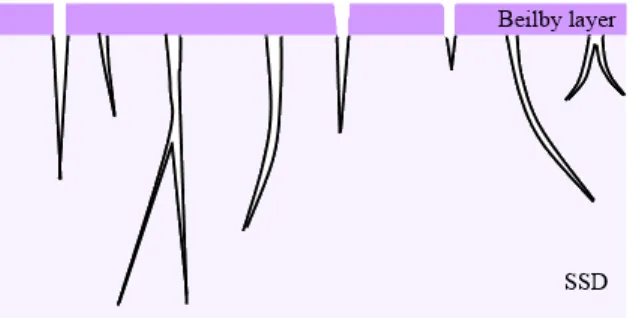
The nature of polished glass interface has attracted significant research in past century. Some of this work was done to support the various hypothesis explaining physical mechanisms at stake in the polishing process: flow theory by Beilby [1], extension of the fine grinding process [2], chemical process [3], etc. Moreover, being able to produce a defect free glass interface has always been and is still a concern for an optical workshop; and this for applications such as lithography, astronomy or high power lasers. In the case of high power laser fused silica optics, these interfacial defects are likely to trigger damage when the optic is submitted to high fluence at 351 nm. Growing of damage under subsequent laser shots limits optic lifetime and induce frequent replacements. Hence, significant effort has been made to improve knowledge of fused silica interface in the past 20 years for this peculiar application. Figure 1 presents a schematic commonly admitted structure of the glass or fused silica interface. Subsurface damage (SSD) consists in an array of subsurface cracks that extends below the surface and is partially covered by the polished layer (or Beilby layer). The former is created during the cutting, sawing and grinding or also by rogue particles during the polishing process. It is due to the action of sharp hard particles on the brittle glass surface acting as indents. The later is due to the chemical-mechanical interactions between the polishing slurry and glass at the final stage of polishing [3] and mainly concentrate contamination coming from tooling and slurries (cerium, alumina, …).
Fig. 1. Schematic structure of the fused silica interface after polishing.
Both SSD and process induce contamination can lead to laser damage at 351 nm. High concentration of ceria in the polished layer induces gray haze e.g. during damage testing [4, 5]. Damage density can thus be linked to pollutant concentration for high degrees of pollution [6]. As depicted in Fig. 1, residual SSD can also lead to laser damage [7, 8].
Optics manufacturing is a multistep process including cutting, grinding, fine grinding, prepolishing, polishing and sometimes intermediate additional operations. Producing a “defect free” interface implies being able to remove at a given step the SSD from the previous one, and generate a shallow SSD as well. Consequently, considerable efforts have been made to be able to estimate the depth of SSD at the various step of manufacturing. The large majority of measurement techniques were established on ground or fine grounded surfaces. At this step of the manufacturing process, the surface is mostly non-transparent as a result of high roughness and high degree of SSD with depth of about ten to hundred micrometers. Measurement methods like local polishing or etching are mostly destructive. A complete bibliography is available elsewhere [9]. Measurement of the interface quality on polished parts is more complex. For SSD, most of the methods valid on non-transparent parts are not efficient on polished parts. Actually, at this step SSD consists in open cracks (visible as scratch and digs on the surface) and subsurface cracks masked by the polished layer (see Fig. 1). Moreover defects density is very low compared to ground/fine grounded surface. Consequently specific methods were developed. For fusion class half meter scale optics, high resolution imaging of the full aperture after a light wet etch can be used but the resolution is limited to some ten micrometers [10]. Raster imaging with a microscope after MRF polishing and light wet etch can improve sensitivity [11]. But this method is destructive and quite complex; moreover these methods suppose that all defects are opened by the wet acid etching. Alternatively Williams used Qdots in the polishing slurry to tag the SSD [12]. Detection is done by confocal microscopy in fluorescence mode. The interest of such a method is that the wet etch step is not needed; the drawback is that dye concentration is rather low and defect tagging is random. Regarding polished layer and more generally process induced pollution embedded in the interface, Secondary Ion Mass Spectrometry (SIMS) [5] as well as wet etching coupled with inductively coupled plasma atomic emission spectroscopy can be used [8].
In this paper, we study interfacial defects existing in polished fused silica surfaces in order to get a better knowledge of their depth and structure. Surface and subsurface defects were created on polished fused silica samples using small silica spherical particles dispersed in a fluorescent liquid dye. Defects on surfaces were counted on the full size sample using a Defects Mapping System (DMS). Width and depth of surface and subsurface cracks were measured using standard fluorescence confocal microscopy or STED confocal microscopy. Results are discussed and confirmed by using magneto-rheological fluid (MRF) finishing to remove defects.
2. Experimental
2.1 Sample preparation
Commercially available 50 mm diameter, 8 mm thick, two-sides polished Corning 7980 fused silica samples were used in this study. Samples have a surface roughness Ra of less than 1 nm
RMS and comply with a 60/40 scratch/dig specification per MIL-O-13830A norm.
Studying defects in polished fused silica glass interface is very difficult. In contrast with ground surfaces, subsurface defects density is rather weak. Moreover the width of fractures is less than a micrometer which is also beyond most of classic optical apparatus resolution. Consequently, groups working on this topic are used to create subsurface defects artificially in large quantity using a process which derives from polishing and uses polishing slurry polluted with large hard particles [11]. The morphology of such artificial imperfections matches well process-related polishing scratches that appear from the last grinding/polishing operations. We retained a similar approach to create subsurface defects on our polished samples. As shown in Fig. 2, an adhesive polishing pad was stuck on a 1.2 kg weight. A slurry containing silica particles of 100 µm diameter dispersed in a D.I. water was preliminary deposited on the sample surface. The weight is moved down to the clamped sample till contact (step 1 of Fig. 2) and is translated one time over the sample surface (step 2 in Fig. 2). Unidirectional scratches with controlled density and width are obtained on the
sample surface. Alternatively, fluorescent dye can also be added to water to make easier subsurface defect measurement (see section 2.3).
Fig. 2. Schematic representation of the experimental method used for the production of polishing-like scratches on sample surfaces.
Typical scratches created by this process are shown on Fig. 3. Image was obtained using a bright field microscope in dark interference contrast mode and a 20x objective. Conchoidal shape, trailing indent fractures are created with morphology similar to polishing process induced scratches [13].
Fig. 3. Typical scratch created by the scratching process.
2.2. Surface defects measurement
In order to observe the result of the creation of scratches on the whole aperture of the samples, a high resolution optical measuring system Defects Mapping System (DMS) was used [10]. It is composed of a 39 Mpx camera, a 120 mm lens and a sample holder coupled to a LED edge illuminating ring. The resulting pixel size is 8 µm with a resolution of 30 µm.
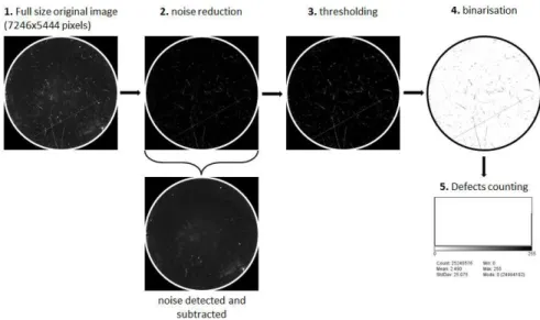
The images were then post-processed using a macro developed with ImageJ [14] in order to quantify the amount of defects. The image analysis process consists in counting the amount of black pixels per cm2 (obscuration), directly related to the amount of defects like scratches.
First of all a noise reduction (rolling-ball algorithm [15]) is applied to the images, followed by a thresholding and a binarisation (see Fig. 4). The amount of black pixels per square centimeter (black pixel density) is finally automatically counted in the selected area of the images.
Fig. 4. Description of the image post-treatment steps using ImageJ.
2.3. Subsurface defects measurement
Subsurface fractures were characterized using confocal microscopy and fluorescence technique. A confocal microscope increases optical resolution and contrast of a micrograph by using point illumination and a spatial pinhole to eliminate out-of-focus light in samples that are thicker than the focal plane. This optical imaging technique enables the reconstruction of 3D structures from the obtained images. Combining confocal microscopy and fluorescence is widely used in biology and cell imaging. These systems are composed of an integrated confocal microscope system consisting of a fluorescence microscope, laser light sources, a scan head to direct the laser on the sample, photodetectors to collect the emission and a computer with dedicated software for controlling the scan head and display the acquisition. Such a confocal microscope can be used in several modes, epi-fluorescence laser scanning mode (ELSM), reflection mode and transmitted mode. The two first ones were used in this study. More details concerning optical path and detection has been published elsewhere [16].
We performed our measurements with a Leica TCS SP8 [17]. All images were made using a 405 nm laser diode (fluorescence mode) and a white light laser (reflection mode), combined to a 63 x objective (NA = 1.4). Typical resolutions of approximately 150 nm in x-y and 300 nm in z are reached. 3D reconstitution and image analysis was performed with Imaris software v 6.0 from Biplane Company and ImageJ. Images were made with a scan speed of 400 lines/second and averaging on 3 images, in the (515 nm - 589 nm) spectral band in fluorescence mode and in the (483 nm – 494 nm) spectral band for the reflection mode. Pinhole is 1 airy. This type of apparatus can be used with different fluorescent dye in order to detect peculiar structures or phenomena; we retain the Lucifer Yellow for our application (peak absorption around 430 nm, peak emission around 530 nm).
In addition to ELSM mode confocal microscopy, stimulated emission depletion (STED) confocal microscopy was used to provide higher resolution [18]. This technique breaks the diffraction limit by using stimulated emission to inhibit the fluorescence process of peculiar type of fluorescent dyes. We performed STED measurements using a Leica TCS pulsed STED SP5 and ATTO647N fluorescent dye. We used pulsed ps laser diode at 635 nm for excitation and a Ti:Sa tunable laser for the depletion (deactivation of fluorophores). Typical
resolutions obtained are around 60 nm x-y and 500 nm in z. The objective we use for STED is a 100 x (NA = 1.4). Images were made with a scan speed of 100 lines/second and averaging on 6 images in the (648 nm - 715 nm) spectral band. Pinhole is 1 airy. To enhance image quality, we de-convolved the images stacks with Huygens Software version 4.4 from Scientific Volume Imaging Company. Characteristics of both ELSM and STED used in this study are summarized in Table 1.
Table 1. Characteristics of methods used for subsurface defects measurements.
ELSM STED Instrument Leica TCS SP8 Leica TCS pulsed STED
SP5 Light source in fluorescence mode Laser diode (405 nm) -
Light source in reflexion mode White light laser -
Light source for excitation - Pulsed ps laser diode (635 nm)
Light source for depletion - Ti:Sa tunable laser
Objective 63x (NA = 1.4) 100x (NA = 1.4)
x-y resolution ≈150 nm ≈60 nm
z resolution ≈300 nm ≈500 nm
Scan speed 400 lines/second 100 lines/second
Pinhole 1 airy 1 airy
Spectral band (fluorescence mode) 515 nm - 589 nm -
Spectral band (reflexion mode) 483 nm – 494 nm -
Spectral band (STED mode) - 648 nm - 715 nm
Fluorescent dye Lucifer Yellow ATTO647N
It must be outlined that STED mode enhance lateral resolution only if a signal in ELSM mode has already been detected at the location to be analyzed in STED mode. Thus ELSM fluorescence and Lucifer Yellow tagging was used for most experiments while STED and ATTO647N tagging was limited to experiments needing high resolution on deep cracks.
Finally, since measurements are carried out in fused silica and not on a microscope lamella, depth measured by confocal microscopy in both STED and ELSM mode were corrected by a factor taking into account the NA of the objective, and the refractive indices of matching oil and fused silica.
3. Results and discussions
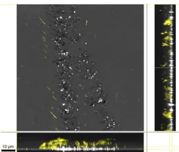
A first set of samples was scratched using the procedure detailed in section 2.1 using silica particles, D.I. water and Lucifer Yellow fluorescent dye for subsurface defects tagging. A typical image obtained in both ELSM mode and reflection mode is shown in Fig. 5. Central image is a top view and includes the entire stack of images. The right side image is a view looking from the left and includes the entire stack. The bottom side image is a side view looking from the top and including all the stacks. Reflection mode signal is represented in black and white, ELSM mode in Yellow. Analysis of top and sides views brings information on surface and subsurface defects. Two main surface scratches created by silica particles are visible. It can also be seen that Lucifer yellow tagging is efficient, allowing imaging of subsurface structures not observed in reflection mode.
Fig. 5. Scratch observed in reflection (black and white scale) and ELSM mode with Lucifer Yellow tagging (yellow scale). Top view (central), side view from left (right) and side view from top (bottom) – All stacks represented.
In the example of Fig. 5, the subsurface defect observed in ESLM mode is associated with a surface scratch. We presume that both scratch and subsurface cracks are created by the action of silica particles acting as indents sticking and slipping on the surface. But such a behavior is not always observed as shown in Fig. 6. In this later less frequent case, no surface defect is observed in reflection mode whereas ESLM signal is present, meaning the existence of subsurface defects. Subsurface defects are here embedded under the polished layer.
Fig. 6. Subsurface defect observed in reflection (black and white scale) and ELSM mode with Lucifer Yellow tagging (yellow scale). Top view (central), side view from left (right) and side view from top (bottom) – All stacks represented.
To confirm this hypothesis, we analyzed a polished sample from the same polishing batch (prior scratching) using Time of Flight (ToF) SIMS. Measurement was performed using O2+
for erosion, analyze is carried out on a 60 x 60 µm2 area. Intensity profiles were normalized by the secondary ion dose. The measurement was repeated at three different locations to
evaluate uniformity with no significant differences observed between profiles. An example of a ToF SIMS profile is given in Fig. 7.
Fig. 7. ToF-SIMS profile obtained on a polished sample. A 50 to 75 nm polished layer is observed.
Process induced contamination of the fused silica glass close surface can be seen with traces of cerium, aluminum and iron (tooling, polishing slurries) but also calcium and potassium (water). Thickness of this contaminated layer is 50 to 75 nm.
Fluorescent dye tagging seems to be an adequate technique for subsurface defect observation. Moreover, 3D observation is here possible in contrast with previous work [12]. But additional experiments are needed to confirm that subsurface fractures are dye tagged to their deepest extend. To assess this point, we made two sets of experiments.
Firstly, we measured the crack width and depth of numerous scratches. Width is defined as the length across the crack on the surface as defined by Suratwala [19]; it was obtained from the reflection mode confocal image. Depth of each crack was measured by analyzing the ELSM mode image stacks. We were then able to represent in Fig. 8 the relation between crack depth (d) and crack width (W).
Fig. 8. Correlation between mean crack depth (d) and crack width (W). Best linear fit is shown in red.
Data linear fitting shows that mean crack depth is linked to width by a d = 0.36 x W relation. This result is in good agreement with the d = 0.35 x W relation established by Suratwala using a destructive method combining MRF wedge polishing to an automatic raster microscope imaging [19]. Consequently dye is likely to penetrate along the full subsurface fracture.
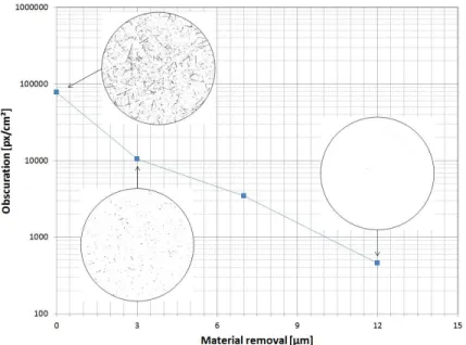
Secondly, a magneto-rheological fluid (MRF) finishing machine was used to suppress created defects from the scratched samples. MRF is a deterministic polishing method that permits local material removal by shear forces created by a fluid in contact with workpiece. It therefore induces very low to almost no SSD during polishing [20, 21]. MRF polishing was realized on a QED Q-22 XE machine using a standard fluid containing cerium oxide particles and a 50 mm diameter wheel. The following parameters were used: wheel speed of 600 rpm, pump speed of 80 rpm, spot depth of about 150 nm. A set of samples was scratched on a LOGITECH PM5 polishing machine using a cerium slurry polluted with 0.1 g/l of 9 µm alumina particles. We verified by confocal microscopy that using this other scratching process the d = 0.36 x W was fulfilled, meaning that similar subsurface defects were created. Iterative MRF uniform layer removals and DMS imaging (see section 2.2) were performed to track subsurface defect removal. Figure 9 shows the evolution of surface obscuration (step 5 of Fig. 4) after iterative material removals on a scratched sample with a mean crack width of 10 µm.
Fig. 9. Evolution of the crack obscuration during iterative material removal. The inserts correspond to DMS images of the initial state and after 3 µm and 12 µm material removal. Light HF wet etch was performed before DMS.
After 3 µm material removal, which approximately corresponds to the mean crack depth of scratches estimated thanks to the d = 0.36 W relation, ImageJ post treatment shows a crack obscuration reduced by a decade. Almost no defects are seen on the DMS imaging thus confirming our depth estimation. DMS analysis using complete removal of any fracture is obtained with a 12 µm material removal which is approximately the crack width. This result is in good agreement with recent results demonstrating that a 90% probability of scratch removal is obtained when removing a depth equal to its width [13].
Based on these two sets of experiments, it is therefore evidenced that most of the subsurface defects are tagged with the dye.
Observations were also carried out in STED mode. For this purpose, samples were scratched using the procedure detailed in section 2.1 using silica particles, D.I. water and
ATTO647N fluorescent dye for subsurface defects tagging. The interest of STED is to improve the resolution of the measurement and consequently gather finer details in the stack. This improvement can be seen in Fig. 10 which compares subsurface fractures evaluated 3 µm below a surface scratch.
Fig. 10. ELSM (left) and STED (right) mode confocal imaging of subsurface fractures, 3 µm below the surface.
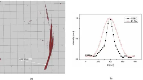
We also used STED stacks of different subsurface fractures to estimate crack width below the surface. An example is given on a single fracture extending about 2.5 µm below the surface and presented in Fig. 11 and in Media 1. A width of 120 nm FWHM (Full Width at Half Maximum) is measured 2.5 µm below the surface in STED mode whereas it is given at 280 nm FWHM in ELSM mode (Fig. 11(b)). Similar sizes can be measured on Fig. 10 on fine details of subsurface fractures and equivalent width are found down to ten micrometers below the surface. This order of magnitude is in good agreement with width of subsurface cracks supposed to play a role in damage initiation at the wavelength of 351 nm [7, 22–24]. For example, Genin et al. demonstrated that 100 nm width and few micrometers depth cracks can induce light intensity enhancements of 10x to 100x depending on their orientation [7].
Fig. 11. Measurement of a subsurface fracture width on an isolated fracture (Media 1) at about 2.5 µm below the surface (a) – X-profile of crack width estimated in ELSM (red circles) and in STED mode (black rectangles) at the pointed location (arrow in (a)) (b).
4. Conclusions
The surface and subsurface defects (i.e. SSD) created during polishing of fused silica parts were investigated by considering artificially created defects similar to those existing on polished glass surfaces. Fluorescent dye tagging of subsurface defects using Lucifer Yellow or ATTO647N during the polishing/scratching process is evidenced to be efficient. Combined with ESLM confocal microscopy, it allows a non-destructive observation of 3D structures of the SSD of polished surfaces. Depths estimated by this method are in good agreement with results from the literature. Combined with STED mode confocal microscopy, it gives access to measurement of fine details of subsurface damage, several micrometers below the surface. This first attempt to use STED on glassy material for this type of observation reveals subsurface fractures of a width of about 120 nm FWHM down to ten micrometers below the surface. Such widths confirm hypothesis about the nature and geometry of damage initiator previously proposed.
Acknowledgments
This work is supported by the Conseil Régional d’Aquitaine and is performed in the framework of the EFESO 2 project. R. Catrin was supported by a CEA/Marie Curie FP7 Eurotalents postdoctoral fellowship.