HAL Id: hal-01520134
https://hal.univ-lorraine.fr/hal-01520134
Submitted on 9 May 2017
HAL is a multi-disciplinary open access archive for the deposit and dissemination of sci-entific research documents, whether they are pub-lished or not. The documents may come from teaching and research institutions in France or abroad, or from public or private research centers.
L’archive ouverte pluridisciplinaire HAL, est destinée au dépôt et à la diffusion de documents scientifiques de niveau recherche, publiés ou non, émanant des établissements d’enseignement et de recherche français ou étrangers, des laboratoires publics ou privés.
Effect of the amorphization around spherical nano-pores
on the thermal conductivity of nano-porous Silicon
Maxime Verdier, David Lacroix, Konstantinos Termentzidis
To cite this version:
Maxime Verdier, David Lacroix, Konstantinos Termentzidis. Effect of the amorphization around spherical nano-pores on the thermal conductivity of nano-porous Silicon. Journal of Physics: Confer-ence Series, IOP Publishing, 2017, 785, pp.12009 - 12009. �10.1088/1742-6596/785/1/012009�. �hal-01520134�
This content has been downloaded from IOPscience. Please scroll down to see the full text.
Download details:
IP Address: 88.86.251.140
This content was downloaded on 09/05/2017 at 17:43 Please note that terms and conditions apply.
Effect of the amorphization around spherical pores on the thermal conductivity of
nano-porous Silicon
View the table of contents for this issue, or go to the journal homepage for more 2017 J. Phys.: Conf. Ser. 785 012009
(http://iopscience.iop.org/1742-6596/785/1/012009)
You may also be interested in:
Depth matters: cells grown on nano-porous anodic alumina respond to pore depth S Thakur, S Massou, A
M Benoliel et al.
Improved Voltage and Fill Factor by Using Zinc Oxide Thin Filmas a Barrier Layer in Dye-Sensitized Solar Cells
Wang Peng, Wang Li-Duo, Li Bin et al.
Photo-ejection and transport of alkali atoms embedded in nano-porous silica A Burchianti, C Marinelli, A Bogi et al.
Temperature of maximum density of water in hydrophilic confinement measured by transient grating spectroscopy
A. Taschin, R. Cucini, P. Bartolini et al.
Nanostructured conducting polymers for stiffness controlled cell adhesion Eric Moyen, Adel Hama, Esma Ismailova et al.
Development of a Functional Chromosome Nano-Dissection System Using Porous Anodic Alumina Pattern Chip and Cantilever
Do-Kyun Kim, Masato Saito, Young-Soo Kwon et al.
Fabrication of Nano-Porous Structure on Silicon Substrate Using Nanoimprint Lithography with an Anodic Aluminum Oxide Nano-Template
Sung-Hoon Hong, Kang-Soo Han, Heon Lee et al.
Simulation and modelling of charge transport in dye-sensitized solar cells based on carbon nano-tube electrodes
Effect of the amorphization around spherical
nano-pores on the thermal conductivity of
nano-porous Silicon
Maxime Verdier, David Lacroix and Konstantinos Termentzidis Universit´e de Lorraine, LEMTA, CNRS-UMR7563, BP 70239, 54506 Vandœuvre Cedex, FRANCE.
E-mail: maxime.verdier@univ-lorraine.fr
Abstract. The thermal conductivity of nano-porous Silicon with amorphous shells around the pores is computed by Molecular Dynamics simulations. For the latter property, a systematic investigation of the porosity and the thickness of the amorphous shells has been performed. Sub-amorphous thermal conductivity is reached for systems with large porosity and amorphous shell, while a non-negligible fraction of crystalline Silicon phase is still present. The thermal conductivity of all studied systems can be controlled by a key parameter which is the ratio of crystalline/amorphous or crystalline/void interface to the volume of material.
1. Introduction
porous semiconductors have been intensively investigated during the last decade. Nano-porous Silicon has possible applications in photovoltaic devices [1] or as a non-toxic and low cost thermoelectric material. Thermal transport through nano-porous systems is often lowered because of phonon scattering on pores’ surfaces. Furthermore, it has been observed that the reduction of the thermal conductivity is more pronounced when the scattering surface per unit of volume is large, i.e. when the porosity is distributed through a high number of small pores [2, 3, 4].
Experimentally, the elaboration of nano-pores is often accompanied by an amorphization around the pores [5]. This might be due to a local reorganization of the atoms around the holes, or to the oxidation of the surface. Amorphous and crystalline phases of semiconductors have very different thermal properties. For instance, the thermal conductivity of bulk crystalline Silicon is 150 W/m.K whereas the bulk amorphous Silicon one is only 1.5 W/m.K (divided by 100) at room temperature. So the presence of an amorphous shell around the pore should have consequences on the global thermal transport, depending upon the shell thickness. A shell of amorphous Silicon around the pore have been modeled by means of Molecular Dynamics simulations in the present work.
First, the geometrical configuration of our systems is described and technical details about the numerical method used to compute the thermal conductivity are given. Then a comparison of the thermal conductivity between nano-porous materials with and without shell around the pores is given. Finally, a key parameter, which can control the thermal conductivity of such systems, is discussed.
Eurotherm Seminar No 108 – Nanoscale and Microscale Heat Transfer V IOP Publishing IOP Conf. Series: Journal of Physics: Conf. Series 785 (2017) 012009 doi:10.1088/1742-6596/785/1/012009
International Conference on Recent Trends in Physics 2016 (ICRTP2016) IOP Publishing Journal of Physics: Conference Series 755 (2016) 011001 doi:10.1088/1742-6596/755/1/011001
Content from this work may be used under the terms of theCreative Commons Attribution 3.0 licence. Any further distribution of this work must maintain attribution to the author(s) and the title of the work, journal citation and DOI.
2. Modeling the structures
The size of the simulation box is constant for all the systems: 10a0 × 10a0 × 10a0 with a0 = 5.43 ˚A the lattice constant, containing 8000 Silicon atoms. One spherical pore is created at the center of the box by erasing some atoms in the specific region. The diameter of this pore can vary from 0 to the dimensions of the box, so the maximum diameter of the pore is 5.43 nm. Periodic boundary conditions are applied on all directions. Thus, we compute the thermal conductivity of an infinite size system with spherical nano-pores periodically spread across the material. A shell of amorphous Silicon can be added around the pore with a “cut and paste technique” [6, 7, 8] . The thickness of the shell can also vary. The thermal conductivity is always computed at room temperature (T = 300 K).
Figure 1. Visualization of a slice of a system modeled with Molecular Dynamics (VMD software [9]). Ge-ometric parameters for this system are: R = 3 a0 and thickness of the amorphous shell t = 0.5 nm. Pe-riodic boundary conditions are ap-plied on all directions.
3. Simulation set up
The simulations are performed with LAMMPS [10]. The time integration is done with Verlet algorithm. The Stillinger-Weber three-body interatomic potential [11] with modified coefficients [12] is used to describe the interactions between the atoms. It has been chosen for its ability to provide an accurate description of thermal transport in both crystalline and amorphous phases of Silicon. The timestep is set to 0.5 fs. Before the main calculation, the system is relaxed to 300 K during 200 ps with a NVT ensemble.
Then the thermal conductivity is computed by Equilibrium Molecular Dynamics (EMD), which is based on the Green-Kubo formula:
kxy = V kBT2 +∞ Z 0 hJx(t)Jy(0)idt (1)
with V the total volume of the simulation box, T the temperature, kB the Boltzmann constant and J the heat flux. The system evolves freely around its equilibrium state under NVT ensemble and the correlation of the fluctuations of the heat flux gives the thermal conductivity. The flux fluctuations are computed each 10 fs and the integral is sampled over 4000 values, so we obtain an estimation of the thermal conductivity every 40 ps. The total duration of a simulation is usually about 10 ns. Each computation is replicated 10 times with different initial conditions in order to reduce uncertainties. This method was validated by retrieving the thermal conductivity of bulk crystalline Silicon (k = 170 ± 21 W/m.K) with different sizes of simulation box. A box of 10a0× 10a0× 10a0 was found to be large enough to guarantee that there is no size effects. 4. Effect of the amorphous shell
In this section, the thermal conductivities of nano-porous Silicon with and without amorphous shell around the pore are compared. In figure 2, the thermal conductivity is depicted as a function of porosity. When the size of the pore is increased, the porosity also increases, as the size of the simulation box is fixed. The thickness of the shell is set to 0.5 nm for all results given
in figure 2. The red line displays the thermal conductivity of bulk amorphous Silicon (about 1.5 W/m.K).
Obviously, the thermal conductivity decreases when the porosity increases, regardless of the presence or not of an amorphous shell. In figure 2, we compare the thermal conductivity of nanoporous Silicon without (black curve) and with amorphous shells (red curve). Systems with amorphous shells have systematically lower thermal conductivity than systems without shells for all the range of the studied porosity. This means that the amorphization around the pore reduces further the global thermal conductivity. This behavior is not surprising as the amorphous shell “crop” a part of the crystalline Silicon domain. This can also be seen when varying the thickness of the amorphous shell while keeping a constant radius of the pore: increasing the fraction of the amorphous phase leads to a greater reduction of thermal transport [13].
Figure 2. Thermal conductivity of nano-porous Silicon with or without amorphous shell around the pores as a function of the porosity. The radius of the pore varies inside a simulation box with fixed dimensions. The shell thickness here is set to 0.5 nm.
The thermal conductivity of some systems presented in figure 2 is extremely low, e.g. for pore’s diameter of 4.3 nm with the amorphous shell, the porosity is greater than 25% and the thermal conductivity is about 1.5 W/m.K. So the ratio of the scattering surface over the volume is very high. For most porous systems with an amorphous shell, we can clearly see in the figure 2 that the thermal conductivity can even reach values below the amorphous limit. Furthermore, for the last point of the red curve, there is still a continuous and non-negligible fraction of crystalline Silicon in the system. When looking at the schematic representation of the system with the biggest pore in the figure 2, one can believe that there is crystalline Silicon only in the corners of the box. But the pore is spherical and this pattern displays a slice of the system in the middle, where the pore size is maximal. So, imagining the real 3-dimension system, it appears that there is still a reasonable fraction of crystalline material (about 13% of the total volume and 27% of the material volume for the last configuration) which form a continuous path between the pores and amorphous shells (a 3D array of interconnected and modulated crystalline nanowires) and may allow the transport of electrons for thermoelectric applications. This extremely low thermal conductivity might be due to the combination of the high density of interfaces (crystalline/amorphous and amorphous/void) and the modifications of the phonon density of states inside the crystalline phase because of the proximity of amorphous material. It has been shown that phonons feel the existence of the crystalline/amorphous interface in a distance of almost 1 nm from the interface [6].
5. Thermal conductivity behavior in nanoporous Silicon, generalization
In order to understand the thermal transport behavior due to the phonons in nano-structured semiconductors with amorphous phase, we have sought a key parameter controlling the thermal conductivity for the studied systems. Usually, for homogeneous and isotropic nano-porous
Eurotherm Seminar No 108 – Nanoscale and Microscale Heat Transfer V IOP Publishing IOP Conf. Series: Journal of Physics: Conf. Series 785 (2017) 012009 doi:10.1088/1742-6596/785/1/012009
materials, the control parameter is taken as the ratio of the scattering surface (the surface of the pores) over the volume of material. In the case of one spherical nano-pore in a periodic and cubic simulation box, this ratio is written as:
S V =
4πR2
L3(1 − φ) (2)
where R is the radius of the pore, L is the dimension of the simulation box (L = 5.43 nm) and φ is the porosity.
Presently, the question is to know how we can consider the presence of an amorphous phase in a general way. In fact, in order to merge all results on the same curve, we have to consider the crystalline/amorphous interface as the main scattering surface:
S V =
4π(R + t)2
L3(1 − φ) (3)
with t the thickness of the shell. So the amorphous/void interface is not considered, it seems to play a minor role in thermal transport. Taking this formula to calculate the ratio S/V when there is an amorphous shell, results for systems with or without shell indeed gather on a same curve (fig. 3). This shows that the crystalline/amorphous interface has roughly the same effect as a crystalline/void interface on thermal transport. Another proof of this assumption is given in our precedent work [13]. Plotting same data as a function of S/V, with S the interface between the material (crystalline or amorphous phase) and the void, the three different systems did not converge on the same curve as previously (fig. 4).
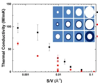
Figure 3. Generalization of the thermal conductivity of nano-porous Silicon with or without amorphous shell around the pores as a function of the ratio S/V, with S the crystalline/amorphous or crystalline/void interface. For systems with the amorphous shell, both “constant thickness - varying radius” and “constant radius - varying thickness” configurations are displayed, and both agree with the generalization.
Figure 4. Thermal conductivity of nano-porous Silicon with or without amorphous shell around the pores as a function of the ratio S/V, with S the surface of the pore. With this parameter, results do not merge on the same curve.
6. Conclusion
Nanoporosity can be used to tune the thermal conductivity by controlling phonons scattering on a dense network of interface. This usually dramatically reduces thermal transport. Moreover, the amorphization of the material which can occur around the pores during the elaboration of nanoporous structures contributes to further decrease the thermal conductivity. This effect is more pronounced when the amorphized zone is large. Adding a shell of amorphous Silicon around very small spherical nano-pores in crystalline Silicon, one can even reach sub-amorphous thermal conductivities while keeping a continuous part of crystalline phase. It is expected that a similar effect would be observed with oxidation around the pores (amorphous SiO2).
Finally, the behavior of the thermal conductivity of nanoporous structures with and without amorphous shells can be universalized with the surface to volume ratio by considering the amorphous/crystalline interface as the main scattering surface for phonons when a shell encloses the pores. This shows that void and amorphous phase globally disturb thermal transport in composite nano-structures in the same way.
Acknowledgments
Authors would like to acknowledge to Dr. A. France-Lanord (CEA Material Design) for support and for many helpful discussions through-out this study. Calculations were performed on the Ermione cluster (IJL-LEMTA).
References
[1] David L. Andrews and Gregory D. Scholes, editors. Comprehensive nanoscience and technology. Elsevier, Acad. Press, Amsterdam, 2011.
[2] J.-H. Lee, J. C. Grossman, J. Reed, and G. Galli. Lattice thermal conductivity of nanoporous Si: Molecular dynamics study. Applied Physics Letters, 91(22):223110, 2007.
[3] Valentin Jean. Mod´elisation du transport de phonons dans les semi-conducteurs nanostructur´es. 2015. [4] David Song and Gang Chen. Thermal conductivity of periodic microporous silicon films. Applied Physics
Letters, 84(5):687, 2004.
[5] M. Isaiev, S. Tutashkonko, V. Jean, K. Termentzidis, T. Nychyporuk, D. Andrusenko, O. Marty, R. M. Burbelo, D. Lacroix, and V. Lysenko. Thermal conductivity of meso-porous germanium. Applied Physics Letters, 105(3):031912, July 2014.
[6] A. France-Lanord, S. Merabia, T. Albaret, D. Lacroix, and K. Termentzidis. Thermal properties of amorphous/crystalline silicon superlattices. Journal of Physics: Condensed Matter, 26(35):355801, September 2014.
[7] A. France-Lanord, E. Blandre, T. Albaret, S. Merabia, D. Lacroix, and K. Termentzidis. Atomistic amorphous/crystalline interface modelling for superlattices and core/shell nanowires. Journal of Physics: Condensed Matter, 26(5):055011, February 2014.
[8] E. Blandre, L. Chaput, S. Merabia, D. Lacroix, and K. Termentzidis. Modeling the reduction of thermal conductivity in core/shell and diameter-modulated silicon nanowires. Physical Review B, 91(11), March 2015.
[9] William Humphrey, Andrew Dalke, and Klaus Schulten. VMD – Visual Molecular Dynamics. Journal of Molecular Graphics, 14:33–38, 1996.
[10] Steve Plimpton. Fast parallel algorithms for short-range molecular dynamics. Journal of computational physics, 117(1):1–19, 1995.
[11] Frank H. Stillinger and Thomas A. Weber. Computer simulation of local order in condensed phases of silicon. Physical Review B, 31(8):5262–5271, April 1985.
[12] R.L.C. Vink, G.T. Barkema, W.F. van der Weg, and Normand Mousseau. Fitting the StillingerWeber potential to amorphous silicon. Journal of Non-Crystalline Solids, 282(2-3):248–255, April 2001.
[13] M. Verdier, K. Termentzidis, and D. Lacroix. Crystalline-amorphous silicon nano-composites: Nano-pores and nano-inclusions impact on the thermal conductivity. Journal of Applied Physics, 119(17):175104, May 2016.
Eurotherm Seminar No 108 – Nanoscale and Microscale Heat Transfer V IOP Publishing IOP Conf. Series: Journal of Physics: Conf. Series 785 (2017) 012009 doi:10.1088/1742-6596/785/1/012009