HAL Id: hal-01687796
https://hal.archives-ouvertes.fr/hal-01687796
Submitted on 18 Jan 2018
HAL is a multi-disciplinary open access archive for the deposit and dissemination of sci-entific research documents, whether they are pub-lished or not. The documents may come from teaching and research institutions in France or abroad, or from public or private research centers.
L’archive ouverte pluridisciplinaire HAL, est destinée au dépôt et à la diffusion de documents scientifiques de niveau recherche, publiés ou non, émanant des établissements d’enseignement et de recherche français ou étrangers, des laboratoires publics ou privés.
Additively patterned ferroelectric thin films with
vertical sidewalls
Aaron Welsh, Denis Dezest, Liviu Nicu, Susan Trolier-Mckinstry
To cite this version:
Aaron Welsh, Denis Dezest, Liviu Nicu, Susan Trolier-Mckinstry. Additively patterned ferroelectric thin films with vertical sidewalls. Journal of the American Ceramic Society, Wiley, 2017, 100 (3), pp.848-858. �10.1111/jace.14566�. �hal-01687796�
Additively Patterned Ferroelectric Thin Films with
Vertical Sidewalls
1
Aaron J. Welsh, 2Denis Dezest, 2Liviu Nicu, and 1Susan Trolier-McKinstry
1
Materials Science and Engineering Department and Materials Research Institute, The Pennsylvania State University, University Park, PA 16802, USA
2Laboratoire d’Analyse et d’Architecture des Systemes-Le Centre National de la Recherche
Scientifique, University de Toulouse, 31077, France
The functional properties of electroceramic thin films can be degraded by subtractive patterning techniques used for MEMS applications. This work explores an alternative deposition technique, where lead zirconate titanate (PZT) liquid precursors are printed onto substrates in a desired geometry from stamp wells (rather than stamp protrusions). Printing from wells significantly increased sidewall angles (from ~1 to greater than 35 degrees) relative to printing solutions from stamp protrusions. Arrays of PZT features were printed, characterized, and compared to continuous PZT thin films of similar thickness. 300 nm thick printed PZT features exhibit a permittivity of 730 and a loss tangent of 0.022. The features showed remanent polarizations of 26 µC/cm2, and coercive fields of 95 kV/cm. The piezoelectric response of the features produced an e31,f of -5.2 C/m2. This technique was also used to print directly atop
pre-patterned substrates. Optimization of printing parameters yielded pre-patterned films with 90° sidewalls. Lateral feature sizes ranged from hundreds of microns down to 1µm. In addition, several device designs were pre-patterned onto SOI wafers (Si/SiO2/Si with thicknesses of
0.35/1/500 µm). The top patterned silicon was released from the underlying material, and PZT was directly printed and crystallized on the free-standing structures in order to provide actuation and sensing capabilities to the device.
1. Introduction
Thin film electroceramics used as sensors, capacitors, actuators, etc. are patterned into specific geometries, commonly by either a wet1 or dry subtractive patterning approach.2,3 These approaches can reduce overall performance4,5 and/or lifetime6 of the final device in cases where patterning-induced damage is produced. Therefore, it is of interest to consider additive patterning techniques for MEMS applications. Ceramic suspensions, pastes, and solutions have been additively patterned at the macro and meso-scale through the use of inkjet printing7 and screen printing.8 Powder-free solutions have been patterned through soft lithographic techniques.9,10,11,12 Soft lithography utilizes elastomeric polymer stamps/molds to deposit or confine solutions onto a substrate. Printing of a ceramic solution from stamp surface directly onto a substrate, termed microcontact printing, has been used to deposit patterned lead zirconate titanate (PZT) thin films with comparable electrical properties to continuous PZT thin films.13
When printing liquids onto a surface, it is essential that the liquid wet the stamp surface in order to provide reproducible printed shapes. On printing from raised features (protrusions), the wetting angle of the solution on the stamp largely determines the final sidewall angle of the deposited layers.14 Protrusion-printing features, ranging in width from 5 to 500 µm, have been used to pattern PZT features with sidewall angles of ~1°.13 Molding-based soft lithography can produces larger sidewall angles. For example, Martin et al.,15 patterned PZT using micromolding in capillaries with ~10° sidewall angles.
Due to the fact that printing with stamp protrusions yield features with shallow sidewall angles, printing from stamp recesses was investigated as an alternative means to increase sidewall angles of printed features. When printing from stamp recesses rather than stamp protrusions, sufficient pressure must be applied for the recess surface to come into contact with a substrate. Thus, the stamp protrusions act as supports, and only the center of the feature contacts the substrate.16 This printing technique was utilized to deposit PZT thin films on released Si cantilevers for biosensing microelectromechanical (MEMS) devices.17
2. Experimental Procedure
2.1 Recess Printed PZT Film Fabrication
Bilayer polymer stamps of polyurethane/polydimethylsiloxane (PU/PDMS) were made as described elsewhere.13 The hydrophilic nature of the polyurethane surface18 allowed the PZT solution to wet the stamp. The compliant, polydimethylsiloxane (PDMS) backing layer allowed the recesses of the stamps to come into contact with the substrates at lower pressures.
Precursor solutions of Pb(Zr0.52Ti0.48)O3 were purchased from Mitsubishi Materials. The
solution was spun onto the polymer stamps at 3000 rpm for 30 s. An MJB-3 contact aligner was used to align and print the PZT solution onto Pt coated Si wafers from NOVA Electronic Materials. The liquid precursors were dried at 350 °C for 3 min and crystallized at 650 °C for 1 min. The fired film was positioned in the contact aligner, and new PZT layers were printed sequentially on the stack, and heat-treated in the same manner. This process was repeated until the desired thickness was achieved.To enable electrical measurements, Pt top electrodes were
deposited on the PZT features using a lift-off process. The Pt was sputter deposited at room temperature in a Kurt J. Lesker CMS-18 sputter system.
Physical dimensions of the printed films were analyzed with a Gemini LEO 1530 field-emission scanning electron microscope. Film thickness was determined using a Tencor Instruments Alpha-Step 500 surface contact profilometer. An HP 4284A precision LCR meter was utilized, from 0.1 to 100 kHz at a drive amplitude of 0.03 V, to measure permittivity and loss tangent. A Radiant Technologies Multiferroics test system was used to measure the P-E loops of the printed films at 100 Hz. The wafer flexure technique19 was utilized to measure the transverse piezoelectric coefficient, e31,f.
2.2 Patterned Substrate Fabrication
Silicon wafers were reactive ion etched using an inductively coupled plasma, Alcatel Speeder 100 Silicon DRIE at 2800W for 90 sec to create desired patterns into the surface of the wafer. The designs were patterned by using Shipley Megaposit SPR 3012 photoresist. A Cambridge Savannah 200 ALD was used to coat the patterned substrate with 30 nm of hafnia, to act as a chemical diffusion barrier. Finally, a Kurt J. Lesker CMS-18 sputter system was used to sputter 30 nm of titanium and 100 nm of platinum at room temperature, which served as the bottom electrode.
2.3 Released Cantilever Fabrication
The released cantilevers were fabricated from 100 mm diameter silicon on insulator (SOI) wafers with 350 nm device silicon and 1 µm buried SiO2 on 525 µm thick silicon carriers.
30 nm of hafnia was deposited onto the SOI wafer using a Cambridge Savannah 200 ALD. The cantilevers were defined by a Shipley Megaposit SPR 3012 photoresist mask. The top silicon
was etched using an Alcatel Speeder 100 Silicon DRIE at 2800W for 30 sec. The buried SiO2
was removed from under the silicon cantilevers using a BOE 6:1 wet etch for 20 min. Titanium was deposited on the surface of the released cantilevers by room temperature sputtering. The Ti was oxidized at 700 ˚C for 1min in an oxygen atmosphere. A 100 nm Pt bottom electrode was sputtered at room temperature onto the surface of the wafer.
Resonance measurements were performed on the released cantilevers under vacuum using an in-house built Fabry-Perot interferometer described elsewhere.20 The amplitude versus frequency response of the cantilever stack was fitted with a Lorentzian function to determine the resonant frequency of the device.
3. Results and Discussion
3.1 Recess Printing from Patterned Stamps
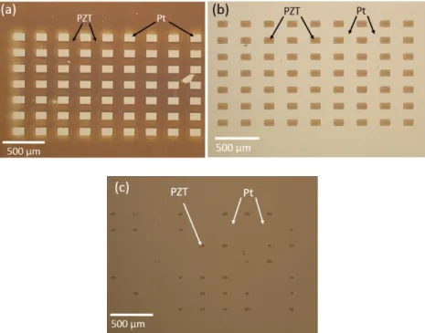
Recess printing requires that both protruding and recess features come into contact with the stamp. In order to avoid deposition of the solution in undesired areas, a sacrificial print was made where only the protruding features contact the surface, as shown in Figure 1 (a). This allows the subsequent printing cycle to deposit only the PZT solution remaining in the stamp wells, as shown in Figure 1 (b). It was found that one sacrificial printing cycle completely removed the PZT precursor solution from the stamp protrusions.
Fig. 1. Optical microscopy images of the (a) initial printing step used to clean the protrusions of the stamp of ceramic precursors, and the subsequent printing of PZT precursor solution from the recesses of the stamp with (b)
1.2 µm and (c) 3.6 µm deep wells. The PZT features are darker in color.
When printing from the recesses of wells, the wells must be shallow enough to allow the well surfaces to come into contact with the substrate, while also being sufficiently deep to insure that the recesses do not touch the surface of the substrate during the sacrificial printing step. The stiffness of the polyurethane, coupled with the inherent undulation of the stamp surface, impose restrictions on the ideal recess depth of the stamp. This work used recesses with areas that were 120 x 78 µm, and each recess was separated from the next by over 100 µm. It was found that for a 10.3 µm well depth, the recesses could not be forced into contact with the printing surface. Results from printing using stamps with recess depths of 3.6 µm are displayed in Figure 1 (c). For this case only ~50% of the recesses come into contact with the printing surface, and of the recesses where printing occurred, only ~20% of the printable area was transferred. Stamps with
recess depths of 2.1 µm allowed 100% of the recesses came into contact with the printing surface. The PZT which was transferred onto the printing surface increased to ~60% of the printable area. 100% of stamp well recesses of 1.2 µm depth came into contact with the printing surface, with an increase to ~77% of the printable area being transferred, as shown in Figure 1 (b). Finally, sacrificial printing of stamps with recess depths of 0.5 µm was performed. However, it was not possible to avoid printing from stamp recesses during this initial printing step. Stamps, in this work, therefore had ideal recesses depth from 1 to 2 µm.
A pivotal difference between printing from stamp protrusions and recesses is edge definition of the printed feature. When printing form stamp protrusions, patterns are defined primarily by the stamp surface features. This design is often lithographically defined by either a photoresist mold or a design etched into a surface. As was shown in previous work,13 printed features from stamp protrusions have a typical line edge roughness of a few hundred nanometers.
However, when printing from stamp recesses, the shape of the printed feature is dictated by several stamp parameters which affect how the externally applied stress is experienced locally at the stamp/substrate interface. Because stamp protrusions act as support pillars, feature corners do not fully come into contact with the printing surface even at large applied pressures;21 this results in rounding of corners in the printed feature. Long range surface undulation also results in various stresses being seen by the printing surface across the stamp, leading to inconsistent printing over long ranges (i.e. ~hundreds of microns). Finally, stamp surface roughness plays a crucial role in the printed feature roughness over short ranges (i.e. tens of microns). Surface roughness results in slight variations in the stamp recess depth, producing variations in the applied pressure between the stamp and the substrate, seen particularly at the edge of the printed
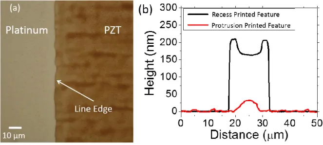
feature. The roughness of the stamps can cause the line edge roughness of features printed from well recesses to be as large as a few microns, as shown in Figure 2 (a).
When printing from a stamp recess, the center of the recess contacts the printing surface. In this configuration the stamp surface does not have a discrete change in surface topography. Hence, the solution should act as a wetting liquid over a flat surface even at the edge of stamp/substrate contact area. This increases the amount of solution available to be transferred along a printed feature edge, and therefore increases sidewall angles in comparison to features printed from stamp protrusions. The surface profile of a 15 µm PZT feature printed from the recess of the stamp is shown in Figure 2 (b), which highlights the difference in the surface profile of PZT printed feature by stamp protrusions and stamp recesses. The features printed from the stamp recess has sidewall angles of ~30°, which is an increase by over an order of magnitude compared to features printed by stamp protrusions.
Fig. 2. (a) Optical microscopy image of the line edge roughness of a PZT feature printed via the recess printing technique. (b) The surface profile of a feature printed from a stamp well (black) in comparison to a feature of similar
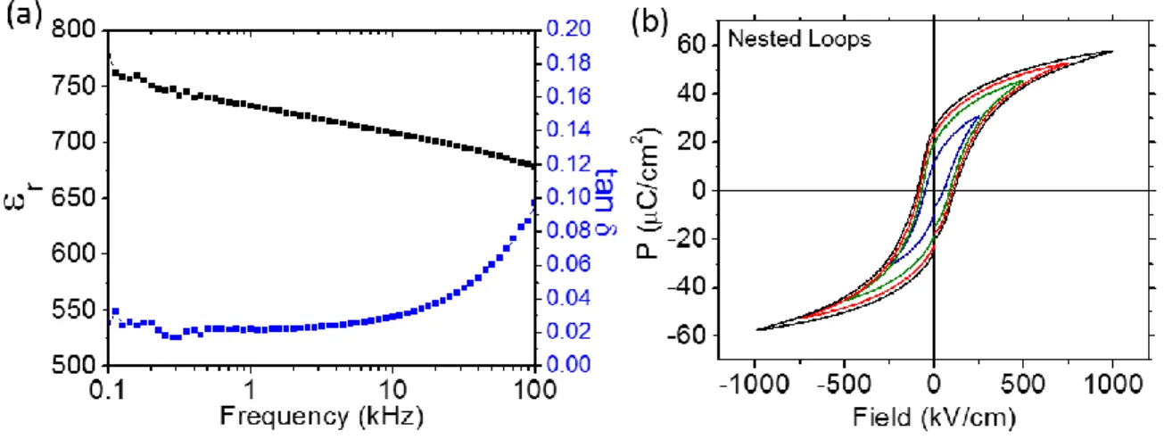
The dielectric, ferroelectric, and piezoelectric properties of a PZT stack deposited through recess printing was characterized. Five recess printed PZT layers yielded a film with a thickness of 300 nm. Figure 3 (a) displays the permittivity and loss tangent as a function of frequency with a permittivity of 730 and loss tangent of 0.022 at 1 kHz. Figure 3 (b) shows the polarization-electric field behavior as a function of increasing electric field. The hysteresis loops are well saturated, with no evidence of pinching or imprint. The printed stack had a coercive field of 95 kV/cm and a remanent polarization of 26 µC/cm2 at 100 Hz.
Fig. 3. Electrical measurements of a recess printed 300 nm PZT stack. (a) Permittivity (black) and loss tangent (blue) as a function of frequency. (b) Hysteresis loop as a function of increasing electric field.
Finally, the transverse piezoelectric coefficient, e31,f, of the film was -5.2 ± 0.3 C/m2. The
dielectric, ferroelectric, and piezoelectric properties of the recess printed PZT film was consistent with the functional properties exhibited by blanket PZT films of similar thicknesses.13 This indicates that the recess printing process does not limit the achievable properties of the patterned features.
3.2 Printing on Patterned Substrates
Printing from stamp recesses onto flat surfaces greatly increases sidewall angles of printed features, but at the cost of increasing line edge roughness. In order to mitigate this problem, a flat stamp can be used to print onto a patterned substrate. In this configuration, the printed ceramic design is dictated by a lithographically defined, dry etched geometry on a substrate. This restricts the line edge roughness of the final printed feature to be on the order of features printed by protrusion stamping. The flat stamps are wetted by the printing solution; effectively making an analogous stamp/solution configuration as the central areas of recesses in patterned stamps. Thus, the increased sidewall angles of the printed features, as exhibited in features printed from stamp recesses, should be preserved in this configuration.
In this work, Pt coated silicon wafers were used as the substrate for printing. Prior to printing, a design was dry etched ~1 µm into the substrate surface. The patterns varied from 500 down to 1 µm in lateral size. Unpatterned composite PU/PDMS stamps were inked with PZT solution and brought into contact with the patterned substrate. Once the stamp was removed, the solution had transferred onto the raised features in the patterned substrate. The precursor film was then pyrolysed and crystallized. This cycle was repeated until the desired thickness was reached. Pre-etching the designs into the surface of the substrate removed the need to align the stamp with the printing surface. Thus, the registry of printing multiple cycles onto a feature became a trivial matter, allowing the printing to be performed by hand.
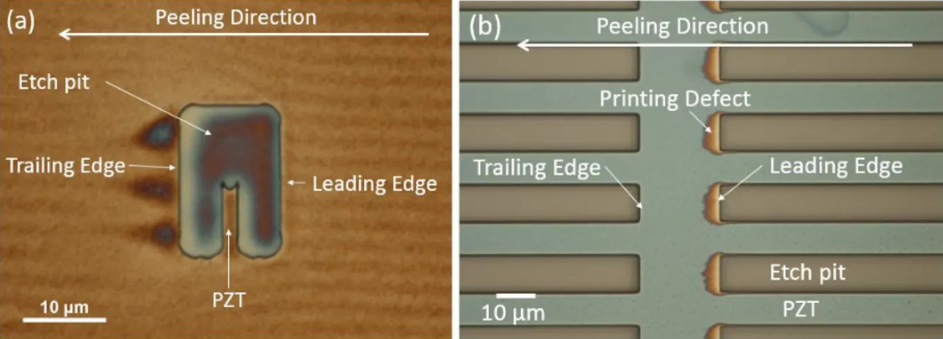
Figure 4 shows PZT solutions that were printed onto patterned substrate surfaces. Figure 4 (a) exhibits the case where a stamp was peeled, from a substrate, from left to right across the feature. The solution clearly experienced redistribution as the stamp was separated from the substrate. The pathlines of the fluid as it interacted with the feature are apparent. On the right
side of the image, the fluid was drawn uniformly across the substrate, but it deformed as it reached the leading edge of the feature, causing the pathlines to curve around the feature. Figure 4 (b) shows an example of a case where the stamp was peeled, from a substrate, from left to right across the feature; enough fluid redistribution has occurred that almost no solution remains on the leading surface of the printed feature. Therefore, it is critical that printing parameters, such as solution viscosity/solution thickness, peeling speed, and peeling direction, be characterized and optimized in order to ensure pattern fidelity over multiple printing cycles.
Fig. 4. Optical microscopy image of a PZT solution printed onto a patterned substrate. (a) Fluid redistribution and (b) printing defects are evident after the stamp was peeled from the substrate from right to left across the features.
The amount of solution that could be transferred from the stamp surface to the patterned substrate surface was investigated. The thickness of the solution deposited onto the stamp surface was varied by controlling the speed of the spin coating from 1000 to 7000 rpm. Following printing, the sample was pyrolyzed and crystallized, and the process was repeated until several hundred nanometers of the PZT film was deposited. The films were cross-sectioned to determine the optimal printing conditions.
Figure 5 (a) shows a 325 nm thick crystallized film where the solution was spun onto the stamp at 1000 rpm. The thickness of the printed film was doubled at the sidewall (~600 nm thick). The printed feature was enlarged, and overhung the original etched feature sidewall by ~200 nm. Figure 5 (b) shows a 275 nm film where the solution was spun at 3000 rpm. The thickness variation of the printed film was only ~25% (~340 nm thick). The film has identical dimensions as the substrate feature with nearly 90 degree printed sidewalls. Films deposited from stamps spun at speeds >3000 rpm did not significantly improve printed sidewall angles or thickness uniformity to justify the decrease in film thickness per layer deposited. In general, ~50 to 60 nm of crystallized PZT thickness per stamping cycle yielded films with steep sidewalls and minimal thickness variation. Thicker coats per print led to significant bulging at feature sidewalls and/or non-uniform solution transfer upon stamp separation from the substrate.
Fig. 5. Cross sectional SEM image of a PZT solution printed onto a patterned substrate. Solution was spun onto stamp at (a) 1000 rpm and (b) 3000 rpm.
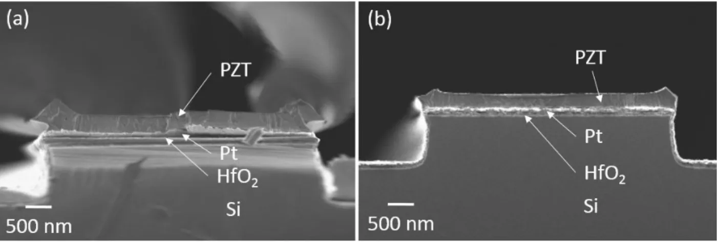
The effect of the peeling direction of the stamp from the substrate in relation to the feature direction was also investigated. Stamps were spin coated with solution at 3000 rpm and brought into contact with a patterned substrate, the stamp was separated from the substrate, and the print was crystallized. Every subsequent print was peeled in the same orientation as the first
printing layer until the final crystallized film was ~300nm thick. The substrate was cross-sectioned to determine the influence peeling direction had on printed feature sidewall angles.
Figure 6 (a) shows a cross-section of a film looking parallel to the peeling direction of the stamp from the substrate feature. In this case, the solution at both right and left sidewalls experience similar dynamic forces upon the separation of the stamp from the substrate. As a result, the printed sidewalls have angles of ~50 to 60°, with an increase in thickness of ~25% (375 nm thick) in comparison to the center of the feature. Figure 6 (b) displays a cross-sectioned film looking perpendicular to the peeling direction of the stamp of the substrate, where the stamp was sperated from right to left across the printed feature. The right printed sidewall in Figure 6 (b) is the leading edge of the patterned substrate, and the first edge to experience the forces associated with the separation of the stamp from the substrate. The solution at this edge is dragged towards the center of the feature, resulting in a printed sidewall angle of ~30°, with an increase in film thickness of ~13% (340 nm thick) at the sidewall. The left printed sidewall in Figure 6 (b) is the trailing edge of the patterned substrate and the final edge to experience the forces associated with the separation of the stamp from the substrate. The solution at this edge is pulled away from the center of the feature, resulting in a printed sidewall of ~60°, accompanied with an increase in film thickness of ~43% (430 nm thick).
Fig. 6. Cross-sectional SEM images of 300 nm crystallized PZT film printed on a patterned substrate feature. The stamp was separated from the substrate (a) parallel and (b) perpendicular to the viewing direction.
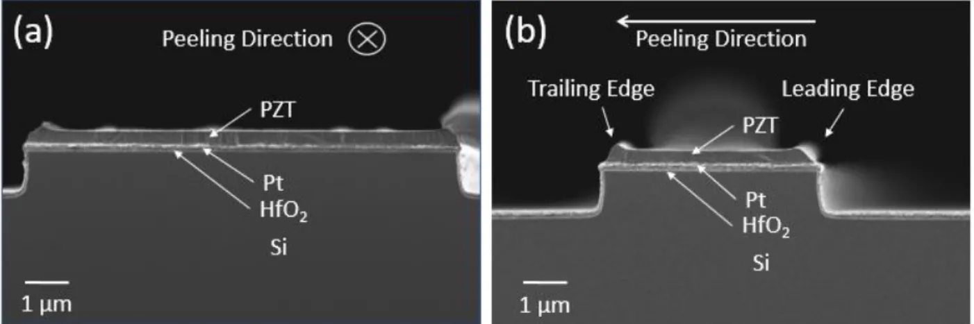
Finally, the peeling rate of the stamp from the substrate was investigated. Stamps were spin coated with solution at 3000 rpm and brought into contact with a patterned substrate, the stamp was separated by hand from the substrate, and the print was crystallized. Every subsequent printing was peeled at the same rate and orientation as the first printing layer until the final crystallized film was ~300nm thick. The films were separated at one of two distinctive peeling rates by hand. In the first case, the stamp was peeled slowly enough away from the stamp that the separation front could be tracked clearly by eye. This separation front was on the order of a few millimeters per second. In the second peeling case, the stamp was removed from the stamp as quickly as possible. In this case, the separation front could not be tracked by eye, but is estimated to be on the order of meters per second based on stamp size and time needed. All crystallized films were cross-sectioned perpendicular to the peeling direction to determine the influence that the peeling rate has on the sidewall angles of printed films.
Figure 7 (a) shows a cross-sectioned film where the stamp was separated slowly (~mm/sec) from a 20 µm lateral substrate feature. In this case, the printed film has shallow
sidewall angles ~20°, however the film has minimal thickness variation across the width of the features. Figure 7 (b) displays the cross-section of a film where the stamp was separated quickly from a 10 µm lateral substrate feature (~m/sec). The sidewalls angles of this printed feature sharply increased to between 70 and 90°. The increased peeling rate also resulted in an ~25% increase in thickness of the printed film near the edges of the feature.
Fig. 7. Cross-sectional SEM images of crystallized PZT film printed with various peeling rates of the stamp from the patterned substrate. Printing was done by hand at peeling rates on the order of (a) millimeters per second or (b)
meters per second. All features had stamp peeling directions parallel to the viewing direction.
It is evident that the fluid dynamics of the solution, as the stamp is separated from the substrate, greatly influences the pattern fidelity of the final printed feature. In this printing technique, the solution is spun onto the stamp as a liquid. During the spinning process, the solution is initially thinned by centrifugal forces generated by the rotating surface. However, this eventually gives way to a the second mechanism for film thinning through solvent evaporation. This causes the film to progressively increase in the concentration of non-volatile constituents as time passes, which in turn greatly increases the viscosity.22 The increase in viscosity results in a gel state. In this work, the evaporation of volatile solvents was evident up to 5 to 10 seconds after
the spinning process. Printing before this evaporation in ambient air was not possible. However, once this gel was formed on the stamp, little to no difference was seen in the printing mechanics whether the printing occurred 30 seconds or 30 minutes after spinning.
The viscous gel state is much more resistant to flow than the original liquid solution. This was most evident in experiments where peeling rates were varied. Slow stamp peeling rates resulted in the gel experiencing low shear rates. This gave the gel adequate time for the high moecular weight organic chains to flow past each other, resulting in printed films where the solution redistributed, resulting in shallow sidewall angles. Fast stamp peeling rates resulted in the gel experiencing high shear rates. This did not allow redistribution of the gel as the stamp was removed from the substrate, producing minimal printing defects and steep sidewall angles.
By tailoring the thickness of each printed layer, alternating peeling directions, and quickly removing stamps from the substrate, it was possible to create printed PZT films with steep sidewalls while minimizing thickness variation across the feature across a wide range of feature sizes. Features printed with optimal printing paramters are shown in Figure 8 (a), which displays a printed 10 µm wide crystallized PZT film with 90° sidewall angles, down to a 1 µm wide printed crystallized PZT film with 70° sidewall angles, shown in Figure 8 (b). These printed films also exhibit excellent perovskite phase formation, showing analogous microstructures to spin-coated PZT films. Figure 8 (c) presents the columnar phase growth of the perovskite phase present in a cross-sectioned 10 µm printed PZT feature with no evidence of porosity. Figure 8 (d) demonstrates, from the top-down view, that printed PZT films exhibit excellent perovskite phase formation, with no evidence of seconday phases or porosity.
Fig. 8. SEM micrographs of crystallized PZT film printed with ideal solution thickness per print, stamp peeling direction, and stamp peeling rate for a (a) 10 µm and a (b) 1 µm. The (c) cross-sectional and (d) top down
microstructure of a crystallized PZT film deposited by printing is displayed.
3.3 Printing on Released Cantilevers
Printing of PZT allows good functional material properties to be retained by avoiding etchants. However, if the device is released after the printed PZT deposition, etchants are usually needed. One way of keeping the functional material from contacting even the releasing etchant is to define and release the structure first, followed by the PZT printing on the released structure.
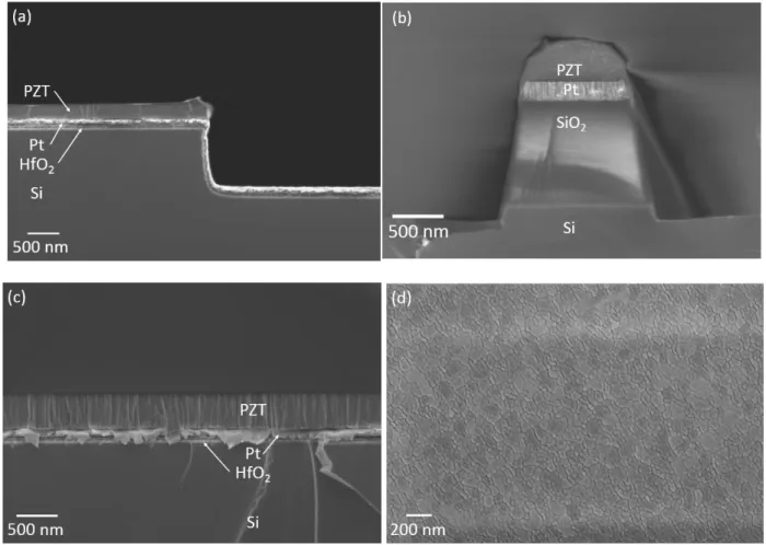
The printing configuration used in this work utilizes a combination of the work described previously. Patterned wells 1.5 µm deep were defined in the stamp surface. 2 and 6 µm wide
cantilevers were defined in the top layer of a SOI wafers by a reactive ion etch down to the buried SiO2 layer. The oxide was subjected to a wet buffered oxide etchant which released the
silicon cantilever from the underlying substrate, as shown in Figure 9 (a). The cantilevers were 350 nm thick and had a 1 µm gap underneath the structure. 30 nm of HfO2 was deposited over
the silicon cantilevers to act as a chemical barrier. The bottom electrode was grown on the cantilevers by first depositing a 30 nm TiO2 adhesion layer for the 100 nm Pt bottom electrode.
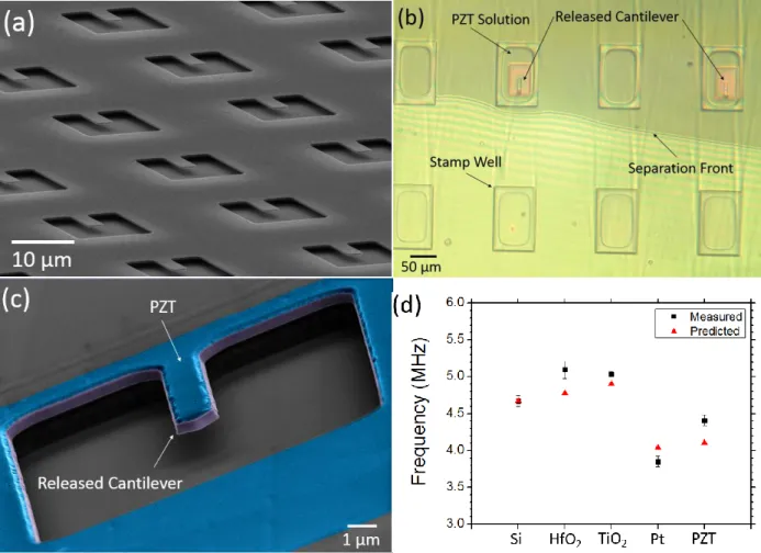
PZT solution was spun onto the patterned stamp surface, and sacrificial printing was performed to remove solution from the protrusions of the stamp. The stamp recesses were aligned with the released cantilever structures. To achieve complete contact with the released structure, enough pressure was applied that the stamp recesses contacted and subsequently forced the cantilever to touch the bottom surface of the cavity in the substrate. The pressure was then slowly reduced until the stamp separated from the wafer, as displayed in Figure 9 (b). Using patterned stamps in conjunction with patterned substrates resulted in PZT solution printed on the top surface of the released cantilever, as shown in Figure 9 (c). This approach also avoids deposition of the PZT in the undesired regions between the released cantilevers, thus avoiding the need for wet etching the PZT from these areas in a subsequent processing step.
Fig. 9. SEM micrographs of (a) released cantilevers which were aligned to a patterned stamp. Optical micrograph of (b) patterned stamp being peeled from released cantilever. (c) Colorized SEM micrographs of the PZT (blue) printed
onto a released 2 µm wide cantilever. (d) Resonant frequency of the released cantilever stack as a function
increasing number of material layers beginning with bare Si and ending with a PZT/Pt/TiO2/HfO2/Si stack.
The printed PZT completely covered the top surface of the released cantilever, while no solution was deposited on the edges of the cantilever. 100% of released structures survived the printing process. It is extremely important to control the direction of separation during stamp removal. If the free end of the cantilever is pulled up along with the leading edge of the stamp, the cantilever can be deflected to a much greater extent than when the cantilever is pressed to the well floor. This can lead to mechanical failure at the base of the structure. However, when the
stamp is removed from the base of the cantilever first, as displayed in Figure 11 (b), the entire structure releases from the stamp more readily. When performed properly, the recess printing of PZT onto released cantilevers showed no visible cracks in either optical or SEM micrographs. 3.4 Mechanical Testing of Released Cantilevers
Measurements of the resonant frequency corresponding to the fundamental mode of vibration of the released cantilevers were conducted to address the question of whether the released structures preserve their mechanical integrity after the PZT deposition. The cantilevers experience large shape deformations during the recess printing of the PZT solutions. These stresses may introduce cracks in the stack that cannot be visually detected or it may introduce subcritical flaws which could cause failure of the beam during device operation conditions. Figure 9 (d) shows that the measured resonant frequency follows the predicted trends before and after PZT deposition. All devices subjected to operational displacement conditions survived testing. These results, coupled with microscopy characterization of the device, suggest that PZT can be printed directly onto released structures to produce useful devices.
4. Conclusions
Printing PZT solutions from the recesses of patterned stamps offers significantly improved sidewall angles in comparison to printing from stamp protrusions; however this comes at the expense of increasing line edge roughness of the printed feature. This was mitigated by defining the feature shape lithographically by etching the desired shape directly into the substrate instead of defining the shape solely into the stamp surface. This produced a printed feature with line edge roughness comparable to features printed with stamp protrusions, but with the added
benefit of increasing sidewall angles by over an order of magnitude. A combination of printing parameters such as thickness of the deposit per layer, peeling direction, and most importantly peeling rate allowed for printed features ranging from hundreds of microns down to 1 µm lateral feature size to exhibit sidewall angles upwards of 70 to 90 degrees. These wall angles are the steepest reported in the literature for ceramic films that have been deposited by an additive patterning technique. Finally, in an effort to produce a free-standing structure where etchants would never see the functional material, printing was performed from stamp recesses directly onto pre-released cantilevers. 100% of the structure survived the stamping process without damaging the mechanical integrity of the resonating device.
4.5 Acknowledgements
The authors gratefully acknowledge funding through the National Security Science and Engineering Faculty Fellowship (NSSEFF) program.
1
K. Zheng, J. Lu, and J. Chu, “A Novel Wet Etching Process of Pb(Zr,Ti)O3 Thin Films for
Applications in Microelectromechanical System,” Jpn. J. Appl. Phys., 43, 3934-37 (2004).
2
K. R. Oldham, J. S. Pulskamp, R. G. Pulcawich, M. Dubey, “Thin-Film PZT Lateral Actuator with Extended Stroke,” Journal of Microelectromechanical Systems, 17, 890-99 (2008).
3
E. Hong, S. Trolier-McKinstry, R. L. Smith, S. V. Krishnaswamy and C. B. Freidhoff, “ Design of MEMS PZT Circular Diaphragm Actuators to Generate Large Deflections,” Journal of
Microelectromechanical Systems, 15, 832-39 (2006).
4
F. Xu, S. Trolier-McKinstry, W. Ren, B. M. Xu, Z. L. Xie, and K. J. Hemker, “Domain Wall Motion and its Contribution to the Dielectric and Piezoelectric Properties of Lead Zirconate Titanate Films,” J. Appl. Phys., 89, 1336-48 (2001).
5
C. W. Chung and C. J. Kim, “Etching Effects on Ferroelectric Capacitors with Multilayered Electrodes,” Jpn. J. Appl. Phys., 36, 2747-53 (1997).
6
W. L. Warren, D. Dimos, B. A. Tuttle, R. D. Nasby and G. E. Pike, “Electronic Domain Pinning in Pb(Zr,Ti)O3 Thin Films and its Role in Fatigue,” Appl. Phys. Lett., 65, 1018-20
(1994).
7
J. Windle and B. Derby, “Ink Jet Printing of PZT Aqueous Ceramic Suspensions,” J. Mat. Sci.
Lett., 18, 87-90 (1999).
8
R. Maas, M. Koch, N. R. Harris, N. M. White, A. G. R. Evans, “Thick-Film Printing of PZT onto Silicon,” Mat. Lett., 31, 109-112 (1997).
9
C. R. Martin and I. A. Aksay, “Submicrometer-Scale Patterning of Ceramic Thin Films,” J.
Electroceram., 12, 53-68 (2004).
10
J. S. Vartuli, M. Ozenba, C. M. Chun, M. Trau, and I. A. Aksay, “Micropatterned Lead Zirconium Titanate Thin Films,” J. Mater. Res., 18, 1259-65 (2003).
11
J. H. Kim, F. F. Lange, and C. I. Choen, “Epitaxial Growth of Patterned SrBi2Ta2O9 Lines by
Channel Stamping,” J. Mater. Res., 14, 1194-96 (1999).
12
N. L. Jeon, P. Clem, D. Y. Jung, W. Lin, G. S. Girolami, D. A. Payne, and R. G. Nuzzo, “Additive Fabrication of Integrated Ferroelectric Thin-Film Capacitors Using Self-Assembled Organic Thin-Film Templates,” Adv. Mater., 9, 891-95 (1997).
13
A. J. Welsh, R. H. T. Wilke, M. A. Hickner, and S. Trolier-McKinstry, “Low-Cost, Damage-Free Patterning of Lead Zirconate Titanate Films,” J. Am. Ceram. Soc., 96, 2799-805 (2013).
14
A. A. Darhuber, S. M. Troian, and S. M. Miller, “Morphology of Liquid Microstructures on Chemically Patterned Surfaces,” J. Appl. Phys., 87, 7768-75 (2000).
15
C. R. Martin and A. Aksay, “Topographical Evolution of Lead Zirconate Titanate (PZT) Thin Films Patterned by Micromolding in Capillaries,” J. Phys. Chem. B., 107, 4261-68 (2003).
16
K. J. Hsia, Y. Huang, E. Menard, J. Park, W. Zhou, J. Rodgers, and J. M. Fulton, “Collapse of Stamps for Soft Lithography Due To Interfacial Adhesion,” Appl. Phys. Lett., 86, 154106 (2005).
17
S. Guillon, S. Salomon, F. Seichepine, D. Dezest, F. Mathieu, A. Bouchier, L. Mazenq, C. Thibault, C. Vieu, T. Leichle, L. Nicu, “Biological Functionalization of Massively Parallel Arrays of Nanocantilevers Using Microcontact Printing,” Sensors and Actuators B: Chemical,
161, 1135-38 (2012).
18
N. Y. Lee, J. R. Lim, M. J. Lee, S. Park, and Y. S. Kim, “Multilayer Transfer Printing on Microreservoir-Patterned Substrate Employing Hydrophilic Composite Mold for Selective Immobilization of Biomolecules,” Langmuir, 22, 7689-94 (2006).
19
J. F. Shepard, P. J. Moses, S. Trolier-McKinstry, “The Wafer Flexure Technique for the Determination of the Transverse Piezoelectric Coefficient (d31) of PZT Thin Films,” Sensors and
20
D.W. Carr and H. G. Craighead, “Fabrication of Nanoelectromechanical Systems in Single Crystal Silicon Using Silicon on Insulator Substrates and Electron Beam Lithography,” J. Vac.
Sci. Technol. B, 15 2760-4 (1997).
21
Y. Y. Huang, W. Zhou, K. J. Hsia, E. Menard, J. Park, J. A. Rodgers, and A, G. Alleyne, “Stamp Collapse in Soft Lithography,” Langmuir, 21, 8058-68 (2005).
22
L. E. Scriven, “Physics and Application of Dip Coating and Spin Coating,” Mat. Res. Soc.