Comparator Design and Analysis for
Comparator-Based Switched-Capacitor Circuits
by
Todd C. Sepke
B.S., Michigan State University (1997)
S.M., Massachusetts Institute of Technology (2002)
Submitted to the Department of Electrical Engineering and Computer
Science in partial fulfillment of the requirements for the degree of
Doctor of Philosophy in Electrical Engineering and Computer Science
at the
MASSACHUSETTS INSTITUTE OF TECHNOLOGY
September 2006
@ Massachusetts Institute of Technology 2006. All rights reserved.
Signature of A uthor ... .... ...
Department of Electrical Engineering and Computer Science
September 29, 2006
Certified by...
. . . . . . ... . . . .. .. . . . .Hae-Seung Lee
Professor of Electrical Engineering
/9
Thesis Supervisor
C ertified by .
....
.
...
Charles G. Sodini
Accepted by
7··//
) rofesso~e
of Electrical Engineering
. .... '- - - '%.."
'V•)•
q,,,-,A,-,r~r•,,,-r~.J±.JLLJ3
kJ LIV V .LL'.JArthur C. Smith
Chairman, Department Committee on Graduate Students
Department of Electrical Engineering and Computer Science
ARCHVES
6
MASSACHUSETTS
INSTIUTE
OF TECHNOLOGYAPR 3 0 2007
LIBRARIES
,· . -.. , .: .. .. . .. ,, . ... . ...i
p-I
Comparator Design and Analysis for Comparator-Based
Switched-Capacitor Circuits
by
Todd C. Sepke
Submitted to the Department of Electrical Engineering and Computer Science
on September 29, 2006, in partial fulfillment of the
requirements for the degree of
Doctor of Philosophy in Electrical Engineering and Computer Science
Abstract
The design of high gain, wide dynamic range op-amps for switched-capacitor circuits
has become increasingly challenging with the migration of designs to scaled CMOS
technologies. The reduced power supply voltages and the low intrinsic device gain
in scaled technologies offset some of the benefits of the reduced device parasitics.
An alternative comparator-based switched-capacitor circuit (CBSC) technique that
eliminates the need for high gain op-amps in the signal path is proposed. The CBSC
technique applies to switched-capacitor circuits in general and is compatible with
most known architectures. A prototype 1.5 b/stage pipeline ADC implemented in a
0.18 Fým CMOS process is presented that operates at 7.9 MHz, achieves 8.6 effective
bits of accuracy, and consumes 2.5 mW of power.
Techniques for the noise analysis of comparator-based systems are presented.
Non-stationary noise analysis techniques are applied to circuit analysis problems for white
noise sources in a framework consistent with the more familiar wide-sense-stationary
techniques. The design of a low-noise threshold detection comparator using a
pream-plifier is discussed. Assuming the preampream-plifier output is reset between decisions, it is
shown that. for a given noise and speed requirement, a band-limiting preamplifier is
the lowest power implementation. Noise analysis techniques are applied to the
pro-totype CBSC gain stage to arrive at, a theoretical noise power spectral density (PSD)
estimate for the prototype pipeline ADC. Theoretical predictions and measured
re-sults of the input referred noise PSD for the prototype are compared showing that
the noise contribution of the preamplifier dominates the overall noise performance.
Thesis Supervisor: Hae-Seung Lee
Title: Professor of Electrical Engineering
Thesis Supervisor: Charles G. Sodini
Title: Professor of Electrical Engineering
Acknowledgments
First, I would like to thank my wife Carrie for her patience and understanding.
Without her support, I would not have made it. I realize it was not easy having a
graduate student for a husband for 6 years. I look forward to our life after graduation.
I would, like to thank my research advisors and mentors Prof. Harry Lee and Prof.
Charlie Sodini. Their guidance and instruction during my years at MIT made my
graduate career challenging, exciting and rewarding. I am indebted to them for their
time, patience, and support.
I would also like to thank John Fiorenza for listening to me talk about noise for
the last 6 years. It has been nice to have at least one person in the office who had
some idea of what I was talking about and that I could bounce ideas off of. And in
our spare time, I think we may have actually solved some of the worlds problems over
coffee...
I would like to thank Peter Holloway for his assistance, guidance and many
stim-ulating discussions over the last couple of years of my Ph.D, and Prof. Jim Roberge
for taking the time to read my thesis and be on my committee.
I would. like to acknowledge the many members of the Sodini group during my
tenure at MIT. The group who endured the Ph.D. program with me: Anh Pham,
Andy Wang, Lunal Khuon, and Albert Jerng. The many good technical discussions,
the dinners out, the homework, the tapeouts, and finally graduation. To the many
junior members of the group, some who have come and gone and others who must still
carry on: Kevin Ryu, Farinaz Edalat, Nir Matalon, Kartik Lamba, Khoa Nguyen,
Ivan Nausieda, Albert Lin, Jit Ken Tan, Matt Powell and Johnna Powell: it has
been a pleasure to work with all of you. I also cannot forget to mention those who
were senior members when I arrived: Don Hitko, Dan McMahill, Ginger Wang, Iliana
Fujimori Chen, and Pablo Acosta Serafini for helping me when I was new.
Similarly, I would like to acknowledge the members of the H. S. Lee group: former
cube-mate Mark Peng, contemporaries Andrew Chen, Matt Guyton, Albert Chow,
fellow Big Ten alum Mark Spaeth for many great technical and non-technical
con-versations, Lane Brooks for many helpful discussions about CBSC, and the senior
members who welcomed me to the group on their way out: Kush Gulati, Ayman
Shabra, and Susan Luschas.
I have also had the pleasure of meeting many other outstanding individuals during
my time at MIT who are to numerous to name, including my colleagues in the MTL
community and the students on the second floor of Bldg 38.
I would like to acknowledge the MTL Mallards Hockey Team and especially Andy
Fan for his efforts to keep the team going and his inspirational pregame emails.
Hockey with the Mallards was an important part of my MIT education.
I would like thank the administrative assistants Kathy Patenaude, Rhonda
May-nard, and Carolyn Collins who always helped to part the MIT red tape. Marilyn Pierce, who has been of great assistance in all departmental and institute matters. She is always looking out for the graduate students. Debb Hodges-Pabon, her
enthu-siasm is contagious; she has made the MTL a great place to work.
I would like to thank the MTL computer and CAD support staff: Mike Hobbs,
Bill Maloney, and Mike McIlrath for keeping the computing and CAD infrastructure
functioning.
I would like to thank my parents for their continued support and encouragement.
I would like to thank my brother Scott for letting me vent my frustrations when
necessary; it is great to have someone else in the family who really understands the
life of a doctoral candidate.
The author was funded by the MARCO Focus Center for Circuits and System
Solutions (C2S2, www.c2s2.org) contract 2003-CT-888x and the MIT Center for
Integrated Circuits and Systems (CICS). The chip fabrication and packing for the
prototype in this thesis were donated by National Semiconductor.
Dedication
I dedicate this thesis to my Grandmother Beulah T. Fleming (January 6,
1912-August 11. 2006) who passed away during my final days at MIT. Her letters and
phone calls were always a welcome respite from life as a graduate student. I could
always count on her being awake at all hours of the night, eager to hear about recent
events in my life, and willing to share her thoughts on current events or memories of
Contents
1 Introduction
23
1.1 Motivation ...
...
23
1.2 Thesis Organization. ...
...
25
2 Comparator-Based Switched-Capacitor Circuits
27
2.1 Overview ... ... 272.2 CBSC Basic Principle of Operation . ...
27
2.2.1
Sampling Circuit ...
...
28
2.2.2
Op-amp Based Charge Transfer Phase . ...
28
2.2.3
Comparator-Based Charge Transfer Phase . ...
30
2.3 Practical CBSC Gain Stage Charge Transfer . ...
31
2.3.1
Preset Phase
...
...
32
2.3.2
Coarse Charge Transfer Phase ...
...
33
2.3.3
Fine Charge Transfer Phase . ...
35
2.3.4
Overshoot Correction ...
....
36
2.4 Noise Analysis ...
...
..
38
2.5 Ramp Linearity ...
...
38
2.6 Summary ...
...
40
2.6.1
Limitations ...
...
40
2.6.2
Advantages ...
...
41
3 Noise Analysis
43
3.1 Noise Analysis Overview ...
3.2 Wide-Sense-Stationary Noise Analysis . ...
.
.
45
3.2.1
WSS Frequency-domain Analysis . ...
46
3.2.2
WSS Time-domain Analysis . ...
.
.
49
3.3 Non-stationary Noise Analysis ...
...
.
...
51
3.3.1
Non-stationary Time-domain Analysis . ...
52
3.3.2
Noise Initial Conditions ...
..
56
3.3.3
Non-stationary Noise Interpretation . ...
57
3.3.4
Non-stationary Frequency-domain Analysis . ...
58
3.4 Input Referred Noise ...
...
62
3.4.1
Noise Gain ...
...
63
3.5 Periodic Filtering Frequency Domain Model . ...
71
3.6 Noise Aliasing ...
...
..
76
3.6.1
White Noise Aliasing ...
..
.
76
3.6.2
Flicker Noise Aliasing ...
..
.
78
3.6.3
Finite Summation Approximation of Aliased Noise
...
84
3.7 Summary ...
...
..
85
4 Threshold Detection Comparator Design
89
4.1
Overview ...
...
...
...
89
4.2 Threshold Detection Comparators ...
...
91
4.2.1
Specifications . .. ...
...
91
4.2.2
Low Noise Comparator Design ....
...
...
.
92
4.2.3
Preamplifier Design ...
...
98
4.2.4
Threshold Detection ...
...
105
4.3 Summary ...
...
...
115
5 CBSC Prototype Pipeline ADC
117
5.1
Overview ...
...
117
5.2
1.5-bit/stage CBSC Pipelined ADC . ...
117
10
5.2.1
Charging Current Sources ...
.
119
5.2.2
Bit Decision Comparators ...
.
120
5.2.3
Virtual Ground Threshold Detection Comparator ...
.
123
5.2.4
CBSC State Machine ...
....
125
5.2.5
Prototype Test Chip ...
....
126
5.3 Experimental Results ...
...
127
5.4 Summary ...
...
...
..
132
6 CBSC Noise Analysis 133 6.1 Overview ... ... ... 133
6.2 Total Input Referred Noise of Pipeline ADC . ...
133
6.3 Single Pipeline Stage Input Referred Noise . ...
135
6.3.1
Periodic Filtering Model ...
.. . .
136
6.3.2 Threshold Detection Comparator Noise . ...
136
6.3.3
Charging Current Noise ...
..
142
6.3.4
Switch Noise
...
...
149
6.4 Putting It All Together ...
...
152
6.4.1
Complete Noise PSD Estimate . ...
154
6.4.2
Comparison of White Noise Voltage Contributions ...
154
6.5 Summary ...
...
..
158
7 Measured Results of Noise in CBSC 7.1 Overview. ... 7.2 Measurement Method ... 7.3 Results ... ... 7.3.1 ADC Input Referred Noise PSD . . . 7.3.2 Sensitivity of Theoretical Prediction . 7.4 Discussion ... 7.5 Summary . ... 159
..
159
159
.
161
162
..
164
..
170
172
8 Conclusion 173
8.1 Thesis Contributions . . ... . ... ... .. 173
8.2 Future Work ... ... . . .... ... .... ... ... . 174
List of Figures
2-1 Bottom plate open-loop sampling (a) Sampling circuit. (b) Sampling clocks. O1A defines sampling instant to minimize input dependent
charge injection. ... ... .. 28
2-2 Op-amp based switched-capacitor gain stage charge transfer phase. (a.) Switched-capacitor circuit (b) The output voltage exponentially settles to the final value. (c) The summing node voltage exponentially
settles to the virtual ground condition. . ... 29
2-3 Comparator-based switched-capacitor gain stage charge transfer phase. (a) Switched-capacitor circuit with an idealized zero delay comparator. (b) The output voltage ramps to the final value. (c) The summing node
voltage ramps to the virtual ground condition. . ... . 30
2-4 CBSC charge transfer phase timing ... ... 31
2-5 Preset phase (P). (a) Switch P closes. (b) vo grounded and vx set
below VCM ... .... ... 32
2-6 Coarse charge transfer phase (E). (a) Current source I, charges out-put. (b) vo and vx ramp and overshoot their ideal values. ... . 34
2-7 Fine charge transfer phase (E2). (a) Current source 12 discharges
2-8 Overshoot cancellation. (a) CBSC stage with overshoot cancellation. (b) vx node voltage during the charge transfer phase without overshoot correction. The large overshoot during the coarse phase prevents the charge transfer operation from finishing in allowed time. (c) CBSC
stage with overshoot cancellation. ... . 37
3-1 Overview of time-domain and frequency-domain analysis. ... . 45
3-2 Transconductance Amplifier. ... .... 47
3-3 Noise Bandwidth (NBW) for a one-pole system. . ... 48
3-4 Transconductance amplifier operating as an integrator (VH > VT). . . 51
3-5 Large signal response of transconductance device with noise. ... 51
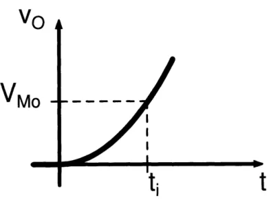
3-6 Step noise signal x(t). Underlying WSS noise process v(t) applied at t = 0. For tl or t2 less than zero, the autocorrelation for x(t) is zero, and for tl and t2 greater than zero, the underlying WSS autocorrelation R,,(tl, t2) defines the autocorrelation of x(t). . ... 52
3-7 Noise initial condition example: capacitor reset noise. (a) RC circuit with capacitor reset noise (R
>
Rswitch). (b) Capacitor RMS noise voltage from initial condition for t > 0. . ... 563-8 In transient noise analysis, it is ensemble averages and not time av-erages that are most important. (a) Ramp voltage plus random walk noise. (b) Average ramp voltage. (c) Random walk noise voltage show-ing 3o bounds. ... ... ... .... .. 59
3-9 Windowed impulse response.... ... . 60
3-10 Frequency Domain: Transfer function for different window widths (ti) 61 3-11 Input referred noise comparator model (a) Noisy comparator results in timing jitter at. (b) Noiseless comparator with input referred noise vn resulting in the same timing jitter. ... ... 63
3-12 Transformation of voltage noise to timing jitter in the comparator de-cision. ... ... . 65
3-14 Response time tj for amplifier to reach output threshold VAMo
. . . . ..68
3-15 Noise Bandwidth versus response time ti.
To=
250 ps ...
69
3-16 Periodic filtering sampler model: the output samples can be modeled
as the impulse train sampling of the input filtered by Fourier transform
of the windowed impulse response. . ...
72
3-17 Periodic integration filter H,(f). DC gain IH,(0)I =
ti/Cs
and
one-sided noise bandwidth NBW
=
1/(2ti). . ...
. .
75
3-18 White noise aliasing NBW
=
3f, .
. . ...
77
3-19 Flicker noise aliasing (a) Original pre-sampled PSD with flicker and
thermal noise. (b) Folded flicker noise. . ...
79
3-20 Total sampled flicker noise PSD showing direct feed-through
contribu-tion and apparent white folded flicker noise. . ...
80
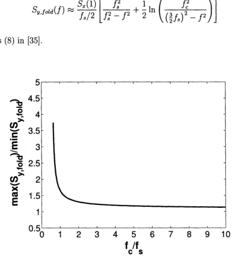
3-21 Maximum to minimum PSD ratio for folded flicker noise. ...
83
3-22 Cumulative aliasing function (CAF): fraction of total noise power as a
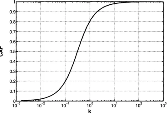
function of the number k of normalized noise bandwidths r. ...
86
4-1 General definition of threshold detection comparator performance. ..
90
4-2 Ideal threshold detection comparator with band-limiting preamplifier.
92
4-3 Ideal timing for comparator with preamplifier. The preamplifier output
voltage is clamped at ±VD. (a) Preamplifier input voltage where the
summing node voltage vx has crossed the virtual ground condition at
time zero. (b) Preamplifier output voltage showing the response time ti
it takes for the preamplifier output to reach the comparator threshold.
(c) Output logic signal changes stage after total comparator delay td.
93
4-4 Holding Gm and CL constant, Ro is swept, the ramp response to a given
threshold VM is faster for high Ro and the total mean-square noise is
lower for high Ro (a) Ramp response. (b) Noise bandwidth... .
96
4-5 Holding Gm and Ci constant, Ro is swept. (a) Ramp response: time to a given threshold VM is faster for larger Ro. (b) Noise bandwidth:
4-6 Relative preamplifier band-limiting capacitance C, versus response time relative to preamplifier time constant x = ti/To for a given noise and
speed requirement. Because Ci is relatively constant, the relative amount of response time is approximately only a function of output
resistance Ro (x - 1/Ro). .
...
...
. 1014-7 Relative preamplifier speed Gm/Ci and transconductance Gm versus output resistance Ro. Transconductance approaches the ideal
integra-tor result versus Ro more quickly than speed. ... 102
4-8 Required preamplifier transconductance versus output resistance for constant noise, speed and linearity requirements. Minimum transcon-ductance (Gm,int) design is an ideal integrator (Ro > Ro,dim). .. . . . 103
4-9 Cascade of three amplifier stages. ... . 106
4-10 Optimum cascade of amplifiers. (a) Optimum number of stages Nop
versus the required gain A for minimum response time ti. Approxi-mation that the gain is a linear function of the natural logarithm of the required gain. (b) Relative delay (ti/lI) versus required gain A
assuming the optimum number of stages Nop is used. . ... 107
4-11 Relative delay versus number of stages for a given gain requirement A. 108
4-12 Current mirror op-amp as a comparator. ... 109
4-13 Bazes comparator based on a self-biased differential amplifier. ... 110 4-14 Inverter with split NMOS and PMOS drive. A source follower is used
as a DC level shifter to drive the NMOS device. ... 111 4-15 Adaptively biased differential amplifier. (a) Simplified schematic. (b)
Re-quired bias current variation. When VID = 0, II = I2. ... 113 5-1 First two stages of Pipeline ADC. Note that the first stage sampling
and bit-decision clocking are controlled by the system clock, but for the second and subsequent stages, the sampling and bit-decision clocking are controlled by the comparator of the previous stage. ... 118
5-2 Coarse and fine phase current sources. Bias voltage generation not
shown. (a) Coarse phase current source II
=
70 kA. (b) Fine phase
current source
12=
3 ýA. ...
...
119
5-3 Bit decision comparators.
(a) Typical cross-coupled inverter based
clocked latch. (b) Cross-coupled inverter based clock latch used in
prototype. Addresses the problem of having to charge node X at the
drain of Mr. (c) Latch timing diagram. . ...
121
5-4 Bit decision comparator data valid and storage registers. ...
.
122
5-5 Schematic of prototype threshold-detection comparator with
band-limiting preamplifier. The total parasitic capacitance at the output of
the band-limiting amplifier determines the bandwidth. Resistors shown
in the schematic are implemented as PMOS devices with grounded
gates operating in the triode region. Each comparator has a power
consumption of roughly 200 kW. ...
..
124
5-6 More detailed schematic of comparator preamplifier for prototype
show-ing the common-mode feedback circuit. . ...
124
5-7 Current source and sampling logic and CBSC state machine. ...
125
5-8 Die photograph. 0.18 pm CMOS process. Pipeline Area: 1.2 mm
2 ..
.
126
5-9 Simplified diagram of the prototype test setup ...
. . . ..
127
5-10 ADC 10b INL and DNL for a 7.9 MHz sampling frequency. (a) DNL.
(b) INL. ...
...
...
129
5-11 Output FFT for f,
=
7.9 MHz sampling rate and a -1 dBFS input at
fi. = 3.8MHz ...
...
...
130
5-12 SNDR and SFDR versus input frequency. . ...
131
6-1 Single 1.5b/stage model for noise analysis. ...
...
134
6-2 Pipeline ADC model noise model. . ...
...
134
6-3 Ideal threshold detection comparator with band-limiting preamplifier.
137
6-4 Half-circuit model for band-limiting preamplifier. (a) Linear half-circuit
model. (b) Waveforms for linear half-circuit model. . ...
138
6-5 Comparator preamplifier for prototype. . ... 138 6-6 Preamplifier response time filter Hw,resp (f)2 for different output
re-sistances causing variation in ti relative to To. . . . . . . 141
6-7 Noise contribution from fine phase charging current 12. . ... 143 6-8 Charging current transfer function during preamplifier response time.
Preamplifier output swept for a constant Gm and Ci. A broad-band preamplifier, lower output resistance, results in more noise cancellation
and therefore, lower transfer function gain. . ... 146
6-9 Noise contribution from sampling and configuration switches. ... 149 6-10 Op-amp based charge transfer switch noise contribution for a gain of
two stage. Op-amp noise bandwidth is 1/(47,) = 2f3dB, C1 = C2 = Cs,
and the load capacitance has been scaled by a factor of two CL = Cs/2. (a) Schematic of op-amp based gain of two stage with switch resistances shown. (b) Input referred noise PSD highlighting feedback v 2, and
feed-forward v2 FF noise paths. ... .. 153
6-11 CBSC versus op-amp based charge transfer timing. Because ti can potentially be made a larger fraction of Ts/2 than the op-amp closed-loop time constant Top can be, for the same power consumption and speed, the comparator-based design has lower noise bandwidth. . . 155
7-1 Theoretical and measured noise PSD fs = 2.4576 MHz, K = 30 . ... 162 7-2 Theoretical breakdown of PSD noise for f, = 2.4576 MHz (a)
Theoret-ical breakdown of aliased components. (b) TheoretTheoret-ical breakdown of
apparent white noise sources. ... ... 163
7-3 Theoretical and measured noise PSD
f,
= 983.04 kHz, K = 30... . 165 7-4 Theoretical and measured noise PSDfs
= 327.68 kHz, K = 30. ... 165 7-5 Fit of ADC input referred noise PSD to determine preamplifier flickernoise parameters. The flicker noise exponent a = 0.86 and the flicker noise PSD for a single preamplifier at 1 Hz Si, (1) = 1.3 x 10⁻¹⁷ A2. . 166
7-6 ADC input referred noise PSD at f = fs/2 and f = df versus flicker noise of preamplifier at 1 Hz Si, (1) ... ... ... . .. . 167 7-7 ADC input referred noise PSD at f = fs/2 and f = df versus flicker
noise exponent a. . ... ... . . 168
7-8 ADC input referred noise PSD at f = f,/2 and f = df versus output
List of Tables
3.1 Fraction of total noise power as a function of the number k of the
normalized noise bandwidths 77
=
[NBW/(f,/2)1 ...
86
5.1 Threshold-detection comparator static bias currents. ...
125
5.2 ADC Performance Summary ...
....
132
7.1
Ranking of apparent white noise sources in ADC PSD estimate for
sampling frequency f,
=
2.4576 MHz. . ...
164
7.2 SNR and ENOB for prototype converter for different combinations of
Chapter 1
Introduction
1.1
Motivation
The design of switched-capacitor circuits in scaled CMOS technologies is becoming increasingly difficult. Although parasitic capacitances are reduced at each successive technology node allowing for faster or lower power operation of analog circuits, other factors such as reduced power supply voltages, lower device output resistance, in-creased flicker noise, and charge leakage paths present challenges to switched-capacitor circuit designers.
Charge storage in scaled CMOS technologies is a looming problem. In the past, only reverse biased diode leakage at the source and drain junction were of concern, but sub-threshold drain current leakage and gate current leakage are becoming sig-nificant'. Existing solutions to this problem involve controlling the bias voltages on devices in their off state to minimize the leakage current [3] [4] [5]. Another alter-native is to operate the circuits faster than otherwise necessary to minimize leakage
charge error
(AQ Oc
Iheak/fs)-Unfortunately, the pocket (halo) implant [6] routinely used in scaled technologies to prevent punch-through and control short channel threshold voltage effects has
1
the unintended side effect of increasing the flicker noise in scaled technologies [7]. Using devices with a larger gate area WL does reduce the input referred flicker noise PSD, but it requires an increase in power consumption to maintain the same speed of operation. Traditional techniques such as correlated double sampling or chopper stabilization can be used to eliminate flicker noise [8], but larger amounts of flicker noise may require performing these functions at frequencies higher than the required Nyquist sampling rate for the input signal bandwidth.
Lower supply voltages reduce the amount of voltage headroom available for the output voltage swing of op-amps. To maintain the same dynamic range, the input referred noise of the op-amp must be reduced. Reducing the op-amp noise requires an increase in the compensation capacitor Cc, but the power consumption must also be increased to maintain the same speed of operation GI/C,.
Another major difficulty in op-amp design for scaled CMOS technologies is the ability to obtain the required DC gain. Devices with shorter channel lengths are expected to have lower output resistance (ro) and intrinsic device gain (gmro), but the pocket (halo) implant [6] also causes a drain-induced threshold shift (DITS) that does not disappear at longer channel lengths [9] [10]. The result is a lower than expected device output resistance even at longer device lengths where DIBL effects are expected to be negligible. Traditionally, the method of obtaining large DC gains with devices that have low output resistance has been to cascode the transistors connected to high impedance nodes in the op-amp. However, cascoding exacerbates the reduced supply voltage problem. The alternative to cascoding is to cascade multiple gain stages, but stabilizing a cascade of amplifiers in feedback is difficult. Techniques such as nested Miller compensation [11] can be used to stabilize the op-amp in feedback, but an increase in power consumption is required to maintain the same speed of operation2 .
To address the issues of low intrinsic device gain and lower supply voltages, a new comparator-based switched-capacitor circuit (CBSC) technique is proposed that eliminates the need for high gain op-amps in the signal path. The proposed
nique is compatible with most known switched-capacitor architectures, but it is more amenable to design in scaled technologies.
1.2
Thesis Organization
Chapter 2 provides an introduction to the comparator-based switched-capacitor tech-nique. This chapter covers the basic principle of operation and a brief discussion of accuracy limitations.
Chapter 3 covers the noise analysis techniques for comparator-based circuits that are use throughout the thesis. The different noise analysis techniques are demon-strated with a series of examples.
Chapter 4 discusses the design of efficient low-noise threshold detection compara-tors. Design equations are presented for a low noise preamplifier for threshold de-tection comparators. Basic threshold comparator design is reviewed, and the unique requirements for threshold comparators in CBSC systems are discussed.
Chapter 5 presents the details and results of the CBSC prototype 1.5b/stage pipeline ADC.
Chapter 6 covers the detailed noise analysis of the CBSC pipeline ADC. The general noise power spectral density (PSD) results for both thermal and flicker noise sources are derived, and the mean-squared noise results for thermal noise sources are also presented.
Chapter 7 presents a comparison between the theoretical noise PSD derived in Chapter 6 and measured results from the prototype.
Finally, Chapter 8 summarizes the contributions of this thesis and suggests areas for future work.
Chapter 2
Comparator-Based
Switched-Capacitor Circuits
2.1
Overview
The basic operation of comparator-based switched-capacitor circuits (CBSC) is in-troduced. After establishing the basics, a more practical comparator-based charge transfer phase is described. Accuracy limitations are introduced, where a further discussion of noise is deferred to later chapters. Finally, a summary of the known limitations and potential advantages of the CBSC technique is given.
2.2
CBSC Basic Principle of Operation
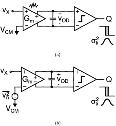
Although the CBSC technique is applicable to a wide range of switched-capacitor circuits, a simple switched-capacitor gain stage is used to illustrate the basic principle of operation. A traditional op-amp based switched-capacitor gain stage is compared to the proposed comparator-based implementation. Both circuits use the same input sampling circuit. The difference is in the method of achieving the virtual ground condition during the charge transfer or amplification phase.
VIN
II EU E u
0-2l
1A
9 A 4
VCM
(a)
(b)
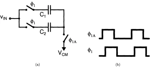
Figure 2-1: Bottom plate open-loop sampling (a) Sampling circuit. (b) Sampling clocks. q1A defines sampling instant to minimize input dependent charge injection.
2.2.1
Sampling Circuit
Assume that both circuits use the same open-loop input sampling circuit shown in Figure 2-1. During the sampling phase 01, the input voltage is sampled onto both C1 and C2. The opening the bottom plate switch to VCM at the falling edge of q1A
defines the sampling instant. The clock &1A is an advanced version of the sampling
phase clock 01. This sampling method minimizes signal dependent charge injection from the sampling switch [13] [14].
2.2.2
Op-amp Based Charge Transfer Phase
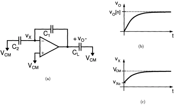
In the traditional op-amp based charge transfer phase, the capacitors C1 and C2
are reconfigured as shown in Figure 2-2. The op-amp then forces a virtual ground condition at node vx. This forces all the charge sampled onto C2 to transfer to C1.
During the charge transfer, both the output voltage vo and the virtual ground node vx exponentially settle to their steady-state values. In Figure 2-2, the exponential settling neglects slew rate limitations and the effects of higher order poles in the op-amp that would increase the required settling time. After a number of time-constants
%I VO
vo[n] -
- ---// ý am-m(m..../0-VCM
VU;M X VCM VCM-(a)
VXo - --.---11 . . . . .(c)
Figure 2-2: Op-amp based switched-capacitor gain stage charge transfer phase. (a) Switched-capacitor circuit (b) The output voltage exponentially settles to the final value. (c) The summing node voltage exponentially settles to the virtual ground condition.
have passed to achieve the desired output voltage accuracy, the output of the stage can be sampled. The relationship between the input and output samples is
vo [n] =( +C2) V[n
- 1]
(2.1)and the capacitor ratio (C2/C1 ) determines the gain of the amplifier.
Note that during the charge transfer phase, the accuracy of the output voltage directly depends on the accuracy of the virtual ground condition. In conventional designs, the op-amp forces the virtual ground in a continuous-time manner, but in switched-capacitor circuits, an accurate virtual ground condition is only required at the sampling instant. Therefore, it should be possible to detect the virtual ground condition at a single time point using a threshold-detection comparator rather than force it with an op-amp. Also, detecting the virtual ground condition should be more
'I
V
0n
VO[n]
VCM VCM VX, VCM VCM-(a)
vXo
-L 4.(c)
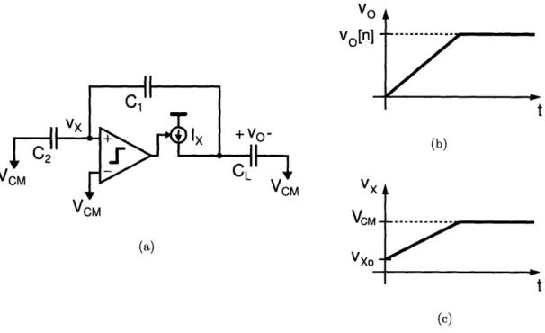
Figure 2-3: Comparator-based switched-capacitor gain stage charge transfer phase. (a) Switched-capacitor circuit with an idealized zero delay comparator. (b) The output voltage ramps to the final value. (c) The summing node voltage ramps to the virtual ground condition.
energy efficient than forcing it.
2.2.3
Comparator-Based Charge Transfer Phase
Detecting the virtual ground condition is the approach taken in the comparator-based charge transfer phase. The procedure for implementing a comparator based charge transfer phase is now presented.
Again, assuming the input was sampled just like in the op-amp case, and the capacitors C1 and C2 are reconfigured in a similar manner; the result is the circuit in
Figure 2-3. The op-amp has been replaced with a virtual-ground threshold-detection
comparator and a current source I.. Assuming for the moment that something
has been done to ensure that vx always starts below the virtual ground condition (Vxo < VCM), the current source Ix turns on at the beginning of the charge transfer
0I.
/o-
(b)
S:
Sample
•2
:
Charge Transfer
P
El
E2
Figure 2-4: CBSC charge transfer phase timing.
phase and charges up the capacitor network consisting of C1, C2 and CL. The ramp
voltage waveforms shown in Figure 2-3 result. The voltage vx continues to increase until it equals VCM. At this point, the comparator detects the virtual ground con-dition and turns off the current source I,. Therefore, the comparator defines the sampling instant. The state of the circuit is identical to that of the op-amp based im-plementation, and the relationship between the input and output samples is identical to (2.1).
2.3
Practical CBSC Gain Stage Charge Transfer
Now that the basic principle of operation has been established, a more practical version like that used in the prototype system is described. The first issue that must be addressed is to ensure the initial condition in the charge transfer phase. The second issue is maximizing the accuracy of the charge transfer phase. To minimize the noise in the comparator decision, it is desirable to maximize the time available to the comparator to do noise averaging when making its decision. The noise averaging property of the comparator is discussed in detail in Chapters 3 and 4. It is also desirable to minimize the final overshoot to minimize the sensitivity to nonlinearity in the ramp rate.
To address these requirements, the charge transfer phase for the prototype was divided into three sub-phases: preset phase (P), coarse charge transfer phase (Ei), and fine charge transfer phase (E2). The time available for each sub-phase is as
illustrated 'in Figure 2-4. The time spent on coarse and fine charge transfer are signal dependent because of the self-timed nature of the comparator-based circuit.
02fli E,
E2
S VOM VCM(a)
(b)
Figure 2-5: Preset phase (P). (a) Switch P closes. (b) vo grounded and vx set below
VCM
2.3.1
Preset Phase
To ensure the voltage vx starts out below the virtual ground condition VCM, a brief preset phase is used. Assuming the input has just been sampled onto Ci and C2, the
summing node voltage vx starts at VCM. If at the same time C2 is connected to VCM, the output node is also switched to the lowest voltage in the system (ground), then a negative step results at the summing node vx through the capacitive divider C, and
C2. This negative step can be used to ensure the preset voltage for vx is less than
the common-mode voltage over a range of input voltages.
To derive the valid input range for the given preset method, the preset value of the summing node voltage vxo is found from its initial voltage VCM and the superposition of the voltage steps at vx from closing the switches at C2 and C, to VCM and ground
respectively1
C1 + C2 C1 + C2
Therefore, the preset value for the summing node is
x= (2 - c
)VcM
- VIN. (2.3)C1 + C2
Using the constraints that the summing node voltage vxo must be greater than zero and less than VCM results in the following valid input range for a gain of two stage
2VcM 5 VIlN- 3 VcM. (2.4)
Assuming that VCM is halfway between the supply rails, this is exactly the same input range required to keep the output within the supply rails.
During the preset phase, the output sampling switch S is also closed after the preset switch to ground has been closed. Therefore, the preset state also resets the
load capacitance before charge transfer begins.
2.3.2
Coarse Charge Transfer Phase
To obtain a quick, rough estimate of the output and virtual ground condition, a relatively fast ramp-rate is used in the coarse charge transfer phase. The coarse phase ramp is generated with current source I1 in Figure 2-6. Because of finite delay of the comparator, the output of the gain stage overshoots the correct value
Vo1=
tdl
(2.5)
CE
1The same result can be derived using charge conservation at the summing node before and after
02
E2
S
II ( VCM VCMFigure 2-6: Coarse charge transfer phase (El). (a) Current source I1 charges output.
(b) vo and vx ramp and overshoot their ideal values.
where I, is the coarse charging current, tdl is the comparator delay for the coarse
charge transfer phase
CE = CL + Cx
(2.6)
and Cx
=
C
1C
2/(C
1+ C2) is the series combination of C1 and C2. The overshoot of
the virtual ground condition is
(2.7)
where
C1fo =
C1 + C 2(2.8)
is the feedback factor.
~ili~
v
I~ --- ~
02 4
I
I
P
I
EF
E2
IV
II I-VcM
t
VXI
Vx°
LIA
VCM VCM . .t
(a)
(b)
Figure
2-7:
Fine charge transfer phase
(E
2).
(a) Current source 12 discharges output.
(b) vo and vx ramp to their final values.
2.3.3
Fine Charge Transfer Phase
To obtain a more accurate virtual ground condition, a fine charge transfer phase with
a significantly more gradual ramp rate is used. The fine charge transfer ramp is
generated with current source I2 in Figure 2-7. The use of the fine charge transfer
phase also erases any noise and nonlinearity from the first comparator decision and
overshoot. It is the final overshoot that determines the offset and nonlinearity of the
stage. If the ramp rate is perfectly constant over the full-scale output range of the
stage, then the final overshoot would only be an offset, and in many systems, it could
be easily be corrected. Unfortunately, the overshoot is not constant in a real system.
Therefore, the second overshoot must be kept small enough to meet the linearity
requirements of the stage.
2.3.4
Overshoot Correction
To maximize the time available for the comparator decision in fine charge transfer phase without placing excessive speed requirements on the comparator during the coarse charge transfer phase, it becomes necessary to implement some sort of over-shoot correction in the coarse charge transfer phase.
Consider the coarse phase decision shown in Figure 2-8(b). If the comparator has a total delay time of tdl for the coarse charge transfer phase, and the reference voltage on the comparator is the common-mode voltage VCM, then the overshoot vov1 of the true virtual condition is relatively large. The fine phase charge current must discharge the summing node voltage back to VcM before the comparator can make its second decision in the fine charge transfer phase. Therefore, the overshoot of VCM limits how much the ramp rate can be reduced for the fine charge transfer phase while maintaining the same speed of operation. However, if the coarse phase ramp rate is constant, then the overshoot vov1 is the same every time, and it is possible to use a comparator reference voltage Voc that is slightly below VCM to anticipate the threshold crossing as shown in Figure 2-8(c). The circuit implementation for the overshoot correction used in the prototype is shown in Figure 2-8(a), where two different references are switched to the comparator for the coarse and fine charge transfer phases.
For a perfectly constant ramp rate, the coarse phase overshoot could be completely canceled, but ramp rate variation and noise in the coarse phase comparator decision place a limit on the amount of overshoot correction. The supply voltages also place
VCM
VOM
C-IVlVoc
VcM
Voc
)V20-w I
tdl
td2Figure 2-8: Overshoot cancellation. (a) CBSC stage with overshoot cancellation.
(b) vx node voltage during the charge transfer phase without overshoot correction.
The large overshoot during the coarse phase prevents the charge transfer operation
from finishing in allowed time. (c) CBSC stage with overshoot cancellation.
2.4
Noise Analysis
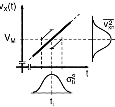
If the comparator is thought of as a finite time integrator,2 then the input referred noise voltage of the comparator is inversely proportional to the square-root of com-parator integration time
1
VnRMS oC 1 (2.9)
This is because the output noise voltage of the integrator preamplifier grows with the square-root of integration time (random-walk)
VoRMS C O
i,
(2.10)but the signal grows proportional to the integration time
vo(t) Oc ti. (2.11)
Noise analysis techniques are covered in Chapter 3. Comparator noise analysis is covered in more detail in Chapter 4 in the context of threshold detection comparator design. Chapter 6 presents the detailed noise analysis of a CBSC gain stage.
2.5
Ramp Linearity
Ramp linearity has an effect similar to finite gain in op-amp based systems. Therefore, careful design of constant ramp generators is key to designing CBSC systems with a high degree of linearity.
2It is shown in Chapter 4 that an integrating preamplifier for the comparator results in the lowest power consumption for a given speed and noise requirement.
In op-amp based designs, the output of a gain stage is
vo = 1(+ 1 )(v"- V.o) (2.12)
1(
1
)
Sfo1
- (VN Vos) (2.13)where fo =: C1/(C1 + C2) is the feedback factor, Vo0 is the input referred offset for the
op-amp, and Ao is the op-amp DC gain.
For the CBSC case, assuming the fine charge transfer phase current source I2 has a constant finite output resistance Ro over the full-scale output range of the stage, I2 can be expressed as
12 = I2o + 1O
(2.14)
Ro
=
I2o 1
+
)
(2.15)
The output ramp rate for the fine charge transfer phase is
dvo
S= 12(2.16)
dt CE
20(
1
+
)
(2.17)
where CE as defined above (2.6) is the net capacitance the current source is charging and is assumed to be constant here. For a comparator delay of td seconds, the final output value is
Vo
_ drv° td(2.18)
V
fo
-
vo
)
N
1(
td )
V
where
Vos
= foI td(2.20)
CE
is the part of the overshoot that is signal independent and looks like an input referred offset voltage. This offset is in addition to the offset of the comparator. Completing the analogy to the op-amp case (2.13), the effective open-loop gain is
CERo
Ao t 0 (2.21)
fotd
The finite output resistance of the fine charge transfer phase current source behaves similar to finite gain in the op-amp case. Note that the gain can be increased in a couple of ways. Shorter comparator delay results in a higher effective gain, but it will trade off with noise performance. Increasing the current source output resistance directly increases the effective gain, and increasing the signal capacitances also helps. Finally, note that unlike the op-amp case, the finite gain term
CERo
Ao
f
o
C
o
(2.22)
td
does not depend of the feedback factor used.
2.6
Summary
The basic principle of a comparator-based charge transfer phase has been explained. Its operation parallels that of an op-amp based system, but it takes advantage of the fact that an accurate virtual ground is only needed at the sampling instant. A brief overview of accuracy limitations was given.
2.6.1
Limitations
Because CBSC systems lack an output amplifier, they can only drive switched-capacitor loads. This is expected since it was one of the drawbacks stated above
for op-amp systems that continuously force the virtual ground and output voltages.
Only being able to drive switched-capacitor loads does not severely limit the
applica-bility of the CBSC approach. If a continuous load needs to be driven, then an output
buffer could be used.
A related limitation is that CBSC designs cannot drive both sides of the sampling
capacitor simultaneously. This makes the technique incompatible with conventional
closed-loop offset cancellation where the input sampling capacitors sample with
refer-ence to a driven virtual ground node. The comparator is still free during the sampling
phase, and other techniques should be possible to perform offset cancellation if
nec-essary.
As discussed above, finite output resistance of the ramp current sources have an
effect similar to finite op-amp gain. However, designing a constant current source in
scaled technologies should be easier than designing a high-gain op-amp because the
current source is not directly in the signal path, and therefore it has fewer design
constraints.
To be sure, the above list of limitations is incomplete. Because this is a new
design method, further investigation is required to determine a more complete list of
limitations.
2.6.2
Advantages
Comparator-based systems have the potential for significant power reduction
com-pared to op-amp based designs because of the differences in the noise-bandwidth and
speed requirements of op-amp and comparator-based designs. See Chapter 4 and [15]
for details.
In addition, comparator-based systems are more amenable to design in scaled
technologies than op-amp based systems because of differences in the requirements
for the comparator and current sources compared to the op-amp. The big difference
is that feedback and stability concerns have been removed for comparator-based
sys-tems, and the high output resistance current sources are not directly in the signal
path.
Finally, the CBSC design method should be applicable to a wide range off
switched-capacitor circuits and compatible with most known architectures. In sampled data
systems, circuit designs that traditionally use feedback to force a virtual ground
should be compatible with the proposed virtual ground detection scheme.
Switched-capacitor filter, integrators, DACs and ADCs should all be compatible with the CBSC
technique. Because the CBSC approach utilizes architectures similar to traditional
op-amp based designs, with some notable exceptions made above, the wealth of the
design techniques and architectures from op-amp designs should transfer to CBSC
designs.
Chapter 3
Noise Analysis
Because of the transient nature of comparator circuits, the usual steady-state anal-ysis that is performed on amplifiers is not appropriate. To determine the transient response of a circuit, differential equations or Laplace transform methods must be employed. These methods are well documented and widely used in electrical engi-neering. Methods for handling transient responses of noise inputs, which are random processes, exist [16] [17], but are not widely known or applied in the electrical engi-neering circuit design community. Two exceptions are the areas of charge transfer devices [18] [19] [20] and relaxation oscillators [21]. The work on charge transfer de-vices actually addresses the more complicated case where device parameters are also allowed to vary with time. This approach is also appropriate for the dynamic circuits discussed here because of their large signal behavior. The linear analysis approach presented in this thesis is only approximate, but it is significantly less complicated than the analysis with time-varying coefficients. The differential equation analysis presented for the relaxation oscillator jitter calculation in [21] is identical in princi-ple to that presented in this chapter. The benefit of the approach presented here is that it generalizes to arbitrary linear, invariant (LTI) systems. The time-domain method presented parallels the usual frequency-time-domain approach. Finally, a set of simple results for the special case of a white noise step input is given with both time-domain and frequency-domain interpretations.
Recently, interest in charge-based sampling circuits [22] that periodically integrate the input signal for a fixed amount of time has resulted in a series of papers applying this technique for sub-sampling [23] [20] [24] [25] [26]. The sampling model and resulting mathematics also apply to the analysis of comparator-based systems if the periodic integration is extended to periodic filtering. While the non-stationary noise analysis examines the details of noise behavior over a single period of operation, a periodic filtering analysis is presented that examines a series of sampled outputs. The sampled values form a wide-sense stationary (WSS) sequence with PSD properties that can be calculated using the traditional frequency domain aliasing model for both thermal and flicker noise sources. Flicker noise is not strictly WSS because the integral of the noise PSD is not bounded on the low frequency limit. However, a finite duration measurement of a flicker noise process is WSS and non-overlapping measurements are independent [27] [28]. This chapter concludes with a brief summary of the key results from noise aliasing theory for both white and flicker noise sources.
3.1
Noise Analysis Overview
Like all signal processing problems, noise analysis can be viewed in the time-domain and the frequency-domain. Both viewpoints tend to offer unique insights to the signal or the system. Figure 3-1 shows a generic system H(f) or h(t) and the input and output quantities associated with frequency-domain and time-domain noise analysis. The quantities shown in the Figure 3-1 and the relationships between them are ex-plained in the following sections. A simple transconductance amplifier example is used to illustrate each analysis method. To keep complexity to a minimum, the series of examples only solve for the output noise voltage. The issues of gain and input referred noise are addressed later in the chapter.
Frequency Domain Analysis
Y(f)
Sy,(f) 2
Gy
Time Domain Analysis
X(f) Sxx(f) 2 ax x(t) Rxx(t ,t2) o2x(t)
Figure 3-1: Overview of time-domain and frequency-domain analysis.
3.2
W ide-Sense-Stationary Noise Analysis
Much like sinusoidal-steady-state signal analysis, steady-state noise analysis methods
assume an input x(t) of infinite duration, which is a Wide-Sense Stationary (WSS)
random process'. A WSS random process has a mean
P:
=
E[x(t)]
(3.1)and variance
oa
=
E
[(x(t) -
Px)2]
(3.2)
that are independent of time. Therefore, the input noise waveform has an ill-defined
amplitude, but it has a constant root-mean-square (RMS) value. In other words, it
has a constant noise power. The RMS value of the noise is commonly measured as a
time average. In circuit analysis, a noise signal is always defined to have zero mean
1Bold variables are used to denote random processes.
y(t)
Ryy(t ,t2)
2
(,x = 0) to separate the deterministic or average response from the noise.
3.2.1
WSS Frequency-domain Analysis
The output y(t) of a linear time-invariant (LTI) system with transfer function H(f) to a noise input can be calculated using the Power Spectral Density (PSD) of the input signal Sxx(f). The output PSD Sy,(f) for the system H(f) can be calculated as
S,,(f) = IH(f)l
2SXX(f)
(3.3)
and the average noise power of the output signal is
2
S,,
(f )
df
(3.4)
y f--c00
Notice that a sided PSD has been assumed in this definition. Because the two-sided PSD Syy(f) is symmetric around zero frequency, a one-two-sided PSD is customarily used
Sx(f)
= 2 S3x(f)
(3.5)
S,(f) =
2
S,,(f)
(3.6)
S,(f) =
IH(f)1
2 SX(f) (3.7)and the integral limits are taken from 0 to +oo
ca2=
S(f) df .
(3.8)
As a final point, the output noise signal also has zero mean and a constant RMS value which means that the output noise is also WSS.
Example 3.1 Transconductance Amplifier: WSS Frequency-domain
0-+
I
I
I
+
Vx
GmV ,
i
R
C
V
Figure 3-2: Transconductance Amplifier.
For comparison to the other analysis methods, the WSS frequency-domain noise analysis of the simple transconductance amplifier in Figure 3-2 is presented. The input noise signal i, is the white noise current source associated with the transconductance device and has a one-sided PSD
Si,(f) = Si,(0) = 4kTGn (3.9)
where Gn, is the noise conductance for the current noise source in. The transfer function from the noise current to the output voltage is simply the impedance that the current source drives
Ro
H(f)= 1 +
j(3.10)
1
+
j27f
TO
where To = R,,C. The output voltage PSD for the amplifier is
So(f) = H(f)|2S ,(f)
= 4kTGn,
(f)2
(3.11)
The usual method to determine the integral for the output noise voltage (3.8) for a white noise input is to define an effective noise bandwidth NBW for the transfer function H(f)
NBW =
)i2
|iH
IH(f)1
2df
(3.12)
10" 10d 10Y 10 10
frequency (Hz)
Figure 3-3: Noise Bandwidth (NBW) for a one-pole system.
which has the well known result for a single pole transfer function
(3.13)
NBW = f3dB =
2 4To
The NBW is shown graphically in Figure 3-3, and it can be thought of as the equiv-alent brick-wall filter bandwidth. The output noise voltage is then
(3.14) Vo = S,, (O) JH(0)12 NBW 1