nanophotonics and quantum optics
The MIT Faculty has made this article openly available. Please share
how this access benefits you. Your story matters.
Citation
Shiue, Ren-Jye et al. “Active 2D Materials for on-Chip
Nanophotonics and Quantum Optics.” Nanophotonics 6, 6 (January
2017): 1329–1342 © 2017 Dirk Englund et al
As Published
http://dx.doi.org/10.1515/NANOPH-2016-0172
Publisher
Walter de Gruyter
Version
Final published version
Citable link
http://hdl.handle.net/1721.1/115283
Terms of Use
Article is made available in accordance with the publisher's
policy and may be subject to US copyright law. Please refer to the
publisher's site for terms of use.
Review article
Open Access
Ren-Jye Shiue, Dmitri K. Efetov, Gabriele Grosso, Cheng Peng, Kin Chung Fong
and Dirk Englund*
Active 2D materials for on-chip nanophotonics
and quantum optics
DOI 10.1515/nanoph-2016-0172
Received October 17, 2016; accepted January 12, 2017
Abstract: Two-dimensional materials have emerged as
promising candidates to augment existing optical net-works for metrology, sensing, and telecommunication, both in the classical and quantum mechanical regimes. Here, we review the development of several on-chip pho-tonic components ranging from electro-optic modula-tors, photodetecmodula-tors, bolometers, and light sources that are essential building blocks for a fully integrated nano-photonic and quantum nano-photonic circuit.
Keywords: optoelectronics; quantum information
pro-cessing; 2D materials; nanophotonics; bolometer; single photon source; photonic integrated circuit.
1 Introduction
Photonic integrated circuits (PICs) allow compact opto-electronic component integration with high stability and low optical losses [1–3]. These properties make them appealing to both classical and quantum information processing applications. However, many applications demand device properties that require multiple disparate materials. For example, light sources must have a larger band gap than photodetectors. Optical modulators rely on materials with a strong electro-optic (E-O) effect [4], and still other materials may be required for non-linear optical functions or non-classical light sources.
Traditionally, the way to approach the problem of inte-grating multiple materials would require heterogeneous material growth or wafer-bonding approaches. However, these approaches can be extremely complex and challeng-ing. For instance, the integration of two types of semicon-ductors – wafer bonding of silicon and III/V InP gain layers – is a major engineering challenge [5]. Two-dimensional (2D) materials, on the other hand, can greatly simplify the assembly of active optoelectronic systems on-chip. They can be conformally layered with relative ease and are “glued” sufficiently strongly by van der Waals (vdW) forces. The advent of such vdW material platforms has proven extremely rich and fruitful for not only electronic [6] but also photonic devices and systems [7]. The primary appli-cations of vdW materials integrated into PICs are in optical interconnects and quantum information processing. Here, we review recent progress in these efforts, focusing on graphene-based E-O modulators and photodetectors, and light sources (classical and quantum) based on 2D transi-tion metal dichalcogenides (TMDCs) and hexagonal boron nitride (hBN). For brevity, we will focus on many areas of our work, but seek to reference other works in the broader context of a wide and rapidly growing research field of 2D vdW materials for quantum optics and optoelectronics. Table 1 summarizes the list of devices that emerge for dif-ferent nanophotonic and quantum photonic applications with different 2D materials (heterostructures).
2 Heterogeneous integration of
2D materials with nanophotonic
devices
Nanophotonic devices, including waveguides and cavi-ties, can control optical fields at subwavelength dimen-sions. Coupling a nanophotonic cavity to a 2D material can enhance light-matter interaction to enable spectrally selec-tive and orders-of-magnitude increased optical absorption and fluorescence. Coupling to nanophotonic waveguides *Corresponding author: Dirk Englund, Department of Electrical
Engineering and Computer Science, Massachusetts Institute of Technology, Cambridge, MA 02139, USA, e-mail: [email protected] Ren-Jye Shiue, Dmitri K. Efetov, Gabriele Grosso and Cheng Peng: Department of Electrical Engineering and Computer Science, Massachusetts Institute of Technology, Cambridge, MA 02139, USA Kin Chung Fong: Raytheon BBN Technologies, Quantum Information Processing Group, Cambridge, MA 02138, USA
Table 1: List of applications of active nanophotonic and quantum photonic devices based on 2D materials.
Applications Materials Band gap Photonics integration Operation mechanism
E-O modulators Graphene Zero gap Waveguides [8, 9] Electro-absorption
Graphene/hBN
heterostructures Zero gap PPC cavities [10] Electro-absorption
Graphene Zero gap Ring resonators [11–13] Electro-absorption Photodetectors Graphene/hBN
heterostructures Zero gap Waveguides [14–16] Photovoltaic and photothermoelectric effects
BP 0.3–2 eV Waveguides [17] Photovoltaic and bolometric effects
(Classical) light
emitters/lasers MoSWSe22, WS2 ~ 2 eV1.5–2.5 eV PPC cavities/micro-disk GaP PPC [18] cavities Purcell enhancement
resonators [19, 20] Purcell enhancement/lasing Bolometers/single
photon detectors Graphene/hBN heterostructures Zero gap PPC cavities Johnson noise thermometry [21] Single photon
emitters hBNTMDCs ~ 6 eV1.5–2.5 eV N/AN/A Atomic defects [22]Atomic defects [23, 24]
provides broadband enhancement. In this section, we discuss theory and experiments of heterogeneously inte-grated 2D materials with optical cavities and waveguides.
2.1 Absorption enhancement in cavity-
integrated 2D materials
Using a temporal coupled mode theory (CMT) that consid-ers the absorption of 2D materials coupling to an optical cavity [25], Gan et al. showed that the reflection, transmis-sion, and absorption of a cavity strongly depend on two
fundamental parameters: the intrinsic cavity loss rate κc
without 2D materials and the excess loss rate introduced
by the absorption of 2D materials κ2D in the cavity. There
are two important regimes for such a coupled 2D materi-als-cavity system: strong attenuation of either the cavity
reflection or transmission with large κ2D/κc ratio and, on
the contrary, maximum absorption in 2D materials with a
critical coupling condition, i.e. κ2D = κc.
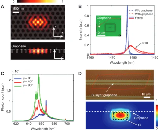
We now discuss an experimental example of the enhanced absorption in graphene integrated with a planar photonic crystal (PPC) cavity. Figure 1A shows the finite-difference time-domain (FDTD) simulation of the cavity field of a PPC cavity fabricated by drilling periodic holes on a suspended gallium phosphide (GaP) membrane (180 nm). The PPC has a lattice constant a of 420 nm with an air-hole radius of 0.29a. A linear three-missing-hole (L3) defect in the middle of the PPC lattice serves to form confined resonant modes. Figure 1B shows the reflection spectrum of the cavity under the illumination of a broad-band (super-continuum laser) source via a cross-polariza-tion confocal microscope. The blue spectrum corresponds to the cavity without graphene deposition, showing a
single sharp resonant peak. The graphene was prepared by mechanical exfoliation and then transferred on top of the cavity [27], as shown in the optical image in Figure 1B. The coupling of the graphene sheet to the evanescent field of the cavity results in reduction of the cavity Q from 2640 to 360, while the resonance red-shifts by 1.8 nm, indicated by the red spectrum acquired after graphene deposition. The cavity reflection dropped by 20 dB at 1477.3 nm (the resonance wavelength of the unloaded cavity). Thus, the naturally weak absorption (2.3%) of graphene [28] from normal incidence is dramatically amplified by coupling to the nanocavity.
From CMT, we deduced the decay rates of κc and κcg
to be 1.9 × 10 − 4 ω
0 and 2.4 × 10 − 2 ω0, respectively [25],
indi-cating that graphene loss accounts for approximately 92% of the total loss inside the nanocavity. By correlat-ing the optical conductivity of graphene to the cavity loss and cavity field distribution, we extracted the single-layer graphene (SLG) complex dielectric function on top of the
cavity to be σg// = 4.64 + 4.62i and σg⊥ = 2.79 at a wavelength of
1477 nm, in good agreement with other reported values [29].
2.2 Fluorescence enhancement of 2D
materials in an optical cavity
Because the local density of optical states is enhanced in a nanocavity, the spontaneous emission (SE) rate of fluorescent materials is also increased, due to the Purcell effect. This Purcell enhancement has been used to greatly improve the SE internal quantum efficiency of 2D mate-rials [18, 30]. Here, we review both experimental results and quantitative analyses of the SE rates of 2D materials coupled to PPC cavities similar to those in the previous
section. These cavities, which are also based on GaP mem-branes, have resonant modes in the wavelength range of 600–700 nm, overlapping with the fluorescence of
molyb-denum disulfide (MoS2), a direct band-gap 2D
semicon-ductor belonging to the group of TMDCs [31, 32].
We measure the fluorescence of the cavity-MoS2
system on a micro-photoluminescence (PL) confocal microscope with a 532-nm continuous-wave excitation laser, focused to a beam diameter of 400 nm with a power of 50 μW. Figure 1C shows the PL collected from the L3 defect, exhibiting several narrow peaks with enhanced
PL intensity compared with MoS2 deposited on a GaP
sub-strate without the cavity. The PL exhibits strong polari-zation dependence, which is resolved by collecting the PL at a polarization angle φ with respect to the cavity along y-axis. Blue, red, and green curves show the PL at φ = 0°,
45°, and 90°, respectively. The two peaks of the MoS2
-cav-ity PL agree to the expected resonant wavelengths, and the polarization dependence of the peaks corresponds well to that of the L3 cavity given by 3D FDTD simulations [33,
34]. The SE rate of the MoS2 in the cavity is proportional to
the Purcell factor, which is a function of the cavity Q and
the effective mode volume Vmode. In this particular sample,
we deduced Purcell factors ranging from 20 to 80 with a cavity Q ~ 300, yielding a maximum seven-fold enhance-ment in the PL intensity.
For other heterogeneous TMDC material systems, Wu
et al. integrated WSe2 with PPC cavity (Q ~ 8000), showing
enhanced Purcell factor of F ~ 600 [19]. Ye et al. coupled
WS2 to the whispering gallery mode of a Si3N4/HSQ
micro-disk resonator [20], and Salehzadeh et al. implemented
MoS2 with SiO2 disk resonators [35]. In the above studies,
strongly enhanced PL in 2D TMDCs resulted in reduced lasing thresholds, promising low-threshold on-chip light sources in 2D materials-based heterostructures. When the coupling rate of the 2D materials to the cavity field becomes even higher, the cavity-2D material coupling enters the strong coupling regime, where the energy of cavity polari-ton mode splits and the excipolari-ton dipoles undergo Rabi
oscillations. Liu et al. observed MoS2 strongly coupled to
a distributed Bragg reflector microcavity [36], showing a Rabi splitting energy of ~ 50 meV.
1460 620 f = 0° ¥ 104 f = 45° f = 90° 0.5 1 1.5 2 640 660 680 Wavelength (nm) Bi-layer graphene 10 µm 1 0 Graphene Si
Photon count (a.u.
) 700 0 0.2 0.4 Intensity (a.u. ) 0.6 0.8 1 1470 1480 Graphene 500 nm A B C D 0 1 Graphene x y x z 10 µm W/o graphene With graphene Fitting Wavelength (nm) 1490 ×10
Figure 1: (A) Simulated electric field distribution of a PPC L3 cavity. Bottom panel shows the cross-sectional view of the cavity mode. The graphene layer on the surface of the suspended PPC membrane can couple to the evanescent field of the resonant mode. (B) Reflection spectrum of a GaP PPC cavity before and after coupling to a single layer of graphene. Inset: Optical image of the graphene-PPC cavity device. (C) Fluorescence of single-layer MoS2 coupled to a PPC cavity [18]. Red, blue, and green curves show the PL collect at a polarization angle of 0°, 45°, and 90°. (D) Top: Optical image of a 70-μm-long graphene couples to a silicon waveguide. Bottom: Simulated waveguide mode couples to the graphene sheet deposited on the top surface of silicon [26].
2.3 Absorption enhancement of 2D materials
integrated with optical waveguides
Thus far, we have described the enhancement of the light-matter interaction via optical resonators. This effect is inherently narrowband due to the narrow resonant bandwidth of the resonators. Coupling 2D materials with a nanophotonic waveguide can enhance the light-matter interaction non-resonantly and hence span a broader bandwidth [16]. The top panel of Figure 1D provides an example device consisting of a bilayer graphene flake deposited across ~ 70 μm over a 520-nm-wide silicon-on-oxide (SOI) waveguide, fabricated from an SOI wafer with a 220-nm-thick Si membrane using the standard shallow trench isolation module. To prevent the graphene from fracturing at the edges of the waveguide, the chip was
pla-narized by backfilling with a thick SiO2 layer and
polish-ing the surface with a chemical-mechanical polishpolish-ing step to reach the top Si layer.
The quasi TE-mode field simulation in the bottom panel of Figure 1D shows the evanescent field overlap to the graphene. From the complex effective index of graphene, we can estimate an absorption coefficient of 0.085 dB/μm. Experimentally, we observed that a 70-μm-long graphene bilayer causes a transmission loss around 6.2 dB over the wavelength range from 1510 to 1580 nm. The transmission loss deduced from the simulation results [16] is ~ 5.95 dB, and we attribute the measured excess loss to the interface scattering between graphene and the waveguide surface.
The absorption coefficient could be greatly increased (to ~ 0.2 dB/μm) by a stronger evanescent field of the wave-guides that support a transverse magnetic guide mode [8, 37] or by thinner waveguides. Other strategies to enhance the absorption include sandwiching the graphene layer inside a dielectric slot waveguide [38] or modifying the electric field distribution by creating an air slot in the middle of a channel waveguide. Wang et al. achieved absorption as high as ~ 1 dB/μm by coupling graphene to such a silicon air-slot waveguide [39].
3 Active optoelectronics
based on PIC-integrated vdW
heterostructures
In the following sections, we discuss 2D materials-based E-O modulators and photodetectors integrated with nano-photonic cavities and waveguides.
3.1 Graphene-cavity high-speed E-O
modulators
Graphene modulators rely on the Pauli blocking effect [40, 41], which is illustrated in Figure 2A. Electrostatic gating
raises (lowers) the Fermi level EF of graphene, causing
reduction in graphene’s optical absorption for photon
fre-quencies ħω < 2 |EF − ECNP|, where EF − ECNP is the difference
in the electron Fermi energy from the charge neutrality point (CNP). Using the Pauli blocking effect in a 50-μm-long SLG coupled to a SOI waveguide [8], Liu et al. demon-strated broadband modulation for wavelengths from 1.35 to 1.6 μm with 3 dB modulation depth. Recently, improved device designs using mutually gated SLG capacitor struc-tures on waveguides achieved modulation depths of 6 dB [9] and 16 dB [42].
Resonators can shrink the size of such graphene ulators. For instance, we demonstrated a graphene mod-ulator based on an air-slot cavity with wavelength-scale mode volume that achieved > 10 dB modulation depth in the telecommunication band [43]. The graphene was gated using an electrolyte layer [poly(ethylene oxide) (PEO) plus
LiClO4], requiring a relatively small swing voltage of 1.5 V
for a modulation contrast of 10 dB.
The relative low speed of electrolyte gating, with a cutoff frequency response < 1 MHz [44], prompted us to develop a high-speed device based on a graphene capacitor on the photonic crystal cavity [10], as illus-trated in Figure 2B. The capacitor consisted of a boron nitride (BN)/graphene/BN/graphene/BN five-layer stack that was produced by the vdW assembly technique and transferred onto a quartz substrate [45], with lower par-asitic capacitance compared to more commonly used
SiO2/Si substrates. The silicon-membrane-based
air-slot PPC cavity was then transferred and aligned with this graphene capacitor, producing the device shown in Figure 2B.
Figure 2C shows the normalized cavity reflection at
λ = 1551 nm as a function of VG, indicating a modulation
depth of 3.2 dB. The modulation for negative bias voltage,
− 5.6 V < VG < 0 V, mimicked that for positive voltage, as the
doping types of the top and bottom graphene layers were reversed. The cavity reflectivity is symmetric about the
CNP at VG = 0.2 V.
The measured E-O S21 parameter, shown in Figure 2D,
indicates a 3 dB cutoff frequency of 1.2 GHz, correspond-ing to the resistance-capacitance (RC)-limited time con-stant of the dual-layer graphene capacitor. A CMT model similar to that described in Section 2.1 indicates that the
real optical conductivity of graphene, σgr, at the maximum
(at the graphene CNP). Thus, a higher contrast would be possible at higher gate voltage, but would push the device
dangerously close to breakdown (Vbreakdown = 0.3–0.8 V/nm
[46, 47]) across the 10-nm-thick BN dielectric layer of the graphene capacitor. Higher contrast could be achieved at longer operation wavelengths, or with the use of high-k materials or chemical doping of the graphene layers near the Pauli blocking regime.
The graphene capacitor in Figure 2 has an area of
~ 100 μm2, a capacitance of 320 fF, and a corresponding
switching energy CV2/2 ~ 1 pJ/bit. Because the graphene
parallel-plate capacitor was much larger than necessary
as the area of the optical mode is only ~ 0.5 μm2,
limit-ing the area of the graphene capacitor to the optical mode (~ 200 times smaller) would lead to a reduction of two orders of magnitude in the switching energy and RC time constant. As the cavity optical bandwidth is large (~ 600 GHz for a Q value of 300), such graphene-PPC modulators could enable high modulation contrast, exceptionally low energy consumption, and a much broader modulation bandwidth than Si modulators based on free-carrier dispersion [48–50].
Several other very promising graphene modulator designs have been introduced. Silicon ring resonators [11, 12] with graphene-based modulation showed a 12.5 dB modulation depth, and a graphene-silicon nitride ring resonator enabled a high modulation contrast of 15 dB per 10 V driving with ~ 30-GHz operation speed [13]. Finally, silicon Mach-Zehnder interferometers have also been
integrated with graphene, producing a modulation depth of > 4 dB and cutoff of 2.5 GHz [51].
3.2 Graphene-waveguide high-responsivity
photodetector
Photodetectors in PICs require a different material that is absorptive where the PIC is transparent. Today, these include epitaxial Ge photodetectors [52], wafer-bonded InP [53], or Si with mid-band-gap states [54]. Graphene has recently emerged as a promising alternative that prom-ises simple layer-transfer integration and photo response from ultraviolet (UV) all the way to the near-infrared, mid-infrared, and terahertz (THz) regimes. Moreover, graphene detectors can be extremely fast – early studies in graphene-based photodetectors show ultrafast pho-toresponse up to 40 GHz with zero bias voltage [55] – and graphene’s strong electron-electron interaction allows multiple hot electron-hole pairs to be generated for each incident photon [56–58], boosting detection responsivity. Recent advances in wafer-scale growth and transfer of graphene are promising for integration of graphene with complementary metal-oxide-semiconductor (CMOS) pro-cesses or with arbitrary materials, likely using back-end-of-line processing steps.
Figure 3A sketches a waveguide-coupled graphene photodetector [15] fabricated on a CMOS-compatible PIC. A stack of 40-μm-long hexagonal BN (hBN)/SLG/hBN,
10–1 –30 –25 –20 –15 –10 –5 0 100 2.5 4 – 3.5 Quartz Au Si PPC cavity Graphene Bottom layer hw/2 hw/2 Top layer A B C D EF BN VG.DC (V ) Frequency (GHz) –5 0.4 0.6 0.8 1 –2.5 Intensity (a.u.) 0 2.5 VG (V ) 5 Electro-optic S21 (dB)
Figure 2: (A) Schematic of the electro-absorptive effects in a capacitor structure consisting of two graphene layers (“top” and “bottom”) separated by hBN. When the Fermi level in graphene rises (drops), the absorption of graphene reduces due to the Pauli blocking of the interband transition of the electrons in graphene. (B) Schematic of the high-speed graphene E-O modulator [10]. (C) Normalized reflection intensity as a function of the gate voltage (VG). (D) Normalized E-O S21 of the graphene E-O modulator as a function of frequency.
transferred onto the PIC using vdW assembly [45], serves as the photodetector. Figure 3C shows the completed structure. The drain electrode is positioned only 200 nm from the waveguide to induce a pn junction [59, 60] near the optical mode [61].
The hBN/SLG/hBN stack decreased the waveguide transmission by 2.2 dB, corresponding to an absorption coefficient of 0.055 dB/μm, consistent with the simulated results for the waveguide evanescent field coupling to the
SLG [16]. We used a polymer electrolyte (PEO and LiClO4)
layer covering the entire chip to independently tune the
Drain Waveguide Source Gate SiO2 Si Graphene A B C hBN SLG hBN 10 µm
Figure 3: (A) Schematic of the graphene/boron nitride heterostruc-ture photodetector integrated with a silicon box waveguide [15]. (B) Cross-sectional view of the side-contacted BN/SLG/BN detector. (C) Optical image of the finished waveguide-graphene photodetector.
0 –2 –4 –6 0 50 100 150 200 250 –0.1 0.1 0.2 0.3 Responsivity (A/W) 0 –1 –0.5 VDS (V) Photocurrent (nA) 0 0.5 A B C D 1 2 4 6 0 2 Experiment Theory 4
Peak power (W) Delay (ps)
Frequency (GHz) 6 –20 100 –9 –6 –3 0 101 60 ps 12 Gbit s–1 102 100 150 200 Photocurrent (nA) Relative response (dB) –10 1.5 W 1.2 W 0.8I W 0.57 W 0 10 20
Figure 4: (A) Photo-responsivity of the graphene detector as a function of drain-source voltage (VDS) and gate-source voltage (VGS). (B)
High-speed response of the photodetector. The red dashed line shows the fitting to the experimental results with an RC low-pass filter model. (C) Photocurrent as a function of peak power under the excitation of pulse laser. (D) Autocorrelation traces of the ultrafast graphene autocorrelator at different peak powers.
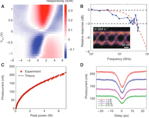
graphene Fermi level and electric field across the wave-guide mode [62–65]. Figure 4A presents responsivity measurements (defined as the ratio of the short-circuit
photocurrent Iph to the optical power Pin in the
wave-guide, i.e. R = Iph/Pin) as a function of VGS and VDS, showing
a six-fold pattern in the photocurrent, which qualita-tively matches the behavior of the photothermoelectric effect [66, 67]. The photocurrent reaches a maximum of
0.36 A/W at VGS = 2 V and VDS = 1.2 V.
The high-speed intensity response of this detector was beyond the capabilities of commonly available E-O modu-lators. As a substitute, we interfered two detuned nar-rowband (1 MHz) telecom lasers to produce an intensity modulation at δf. Figure 4B plots the relative optical-to-electrical response of the detector received on an optical-to-electrical spectrum analyzer (maximum frequency 50 GHz) at differ-ent δf. This measuremdiffer-ent indicates a 3 dB cutoff frequency at 42 GHz, matching the highest reported graphene photo-detector speed [14]. Sending pseudorandom on-off-keyed data produced a clear eye-opening diagram at 12 Gbit/s (inset of Figure 4B).
Waveguide-integrated graphene photodetectors are possible with CMOS-compatible processes [61]. In addition to exfoliated graphene devices, large-scale
chemical vapor deposition-grown graphene integrated with waveguides can achieve a data rate of 50 Gbits/s [14], and high-responsivity by integrating with a silicon air-slot waveguide [39]. Owing to the broad-band absorption of graphene, waveguide-integrated graphene heterostructure also enables photodetectors for mid-infrared wavelengths [68]. For other 2D materi-als, black phosphorus (BP)-based photodetectors have drawn great attention due to their small band gap that is promising for telecommunication and mid-infrared wavelength ranges [17, 69]. Heterogeneously integrated BP-silicon photodetectors have shown up to 6 A/W responsivity with > 3 GHz speed.
3.3 Ultrafast on-chip autocorrelator
The photocurrent presented in the previous section exhibits a non-linear photoresponse with a peak power that is > 50 mW. The power-dependent curve (Figure
4C) fits well by a power law of Iph ∝ Pin0.47, suggesting
supercollision-dominated cooling mechanism [70]. The picosecond-scale non-linear photocurrent is desirable for on-chip optical signal characterization, e.g. ultrafast optical sampling and autocorrelation measurements. In Figure 4D, we plot photocurrent traces as a function of the time delay Δt between pairs of 250-fs laser pulses for a range of incident powers. These traces show a clear dip at
Δt = 0 with a width corresponding to the detector’s carrier
relaxation time of ~ 3 ps. In this device, strong non-linear photoresponse at low peak power could enable a more efficient on-chip autocorrelator compared with existing autocorrelators based on free-space parametric frequency conversion and two-photon absorption in semiconduc-tor waveguides [71–73], while keeping a footprint of only 40 μm in length. The femtosecond thermalization of gra-phene’s hot electrons suggests that the timing resolution of the on-chip autocorrelator is possibly down to sub-50 fs [74]. It is also important to note that this graphene-based autocorrelator supports a broad spectral range from 1500–1800 nm.
3.4 Ultrasensitive graphene-based
bolometers and single photon detectors
With its exceptionally small electronic heat capacity [75– 79] and weak electronic heat dissipation [64], graphene is also a promising material platform for ultrasensitive thermal detectors [80–82]. The exceedingly low number of atoms in a typical graphene device and the vanishing
density of states at the CNP result in a record-low elec-tronic specific heat, which is on the order of one Boltz-mann constant. Hence, a graphene-based bolometer is comparable to some of the best nano-calorimeters [81, 83]. Additionally, the small size of the Fermi surface and the high energy of graphene’s phonons result in a strongly suppressed heat flow from hot electrons into the phonon bath. With these unique thermal properties, gra-phene is a natural heat absorber for bolometer applica-tions and allows for a high temperature rise by incident radiation, even down to the energy quanta of a single photon.
To investigate graphene’s thermal properties and to demonstrate the proof of concept of the graphene bolom-eter, we investigated a Johnson noise thermometry circuit [21, 78, 84] to directly read the electronic temperature using the Johnson-Nyquist theorem. As shown in Figure 5A, the graphene device is impedance-matched with an inductor-capacitor (LC) matching network, which enables maximal transmission of the generated noise power. The signal is further amplified using a state-of-the-art low-noise ampli-fier, resulting in an overall temperature sensitivity that
approaches 0.001 K/Hz1/2. A directional coupler is used to
apply Joule heating pulses and to simultaneously monitor the response of the electronic temperature, which enables direct measurements of the electronic cooling mechanisms
through the study of the electronic thermal conductance Gth.
The heat transfer P is dominated by electron-phonon
cooling and follows a high power law P = σA(Te4 − T
p4),
where σ is the electron-phonon coupling parameter, A is
the graphene area, Te is the electron temperature, and Tp
is the phonon temperature. Figure 5B shows the typical data taken at different temperatures. Through the relation
Gth = P/ΔTe, we can extract the thermal conductance, which
we find to be on the order of 0.2 nW/K (Figure 5C). This corresponds to a noise equivalent power of the bolometer
of 0.4 pW/K at 2K, as given by the product of Gth and the
temperature sensitivity. Using a much cleaner graphene device at the CNP, the bolometer is predicted to reach an
even lower NEP of ~ 10 − 21 W/Hz1/2 [78].
The above extracted parameters make it possible to engineer a graphene-based device that could detect a single photon in the frequency range from UV to GHz. Figure 5D shows a device concept for a thermal graphene-based single photon threshold detector. High quantum efficiency can be achieved by critical coupling of the gra-phene to a photonic crystal cavity. The gragra-phene sheet is further coupled to two closely spaced superconduct-ing electrodes that form a Josephson junction and allow for a supercurrent to flow through the graphene [85–87]. Upon absorption of a single photon, the temperature of
the device is increased above the critical temperature of the superconductor, creating a detectable voltage pulse across the device.
4 vdW materials for single photon
generation
A single photon emitter (SPE) is a critical element for quantum information processes, including quantum networks [88] and photonic quantum computing [89]. Layered materials have recently shown quantum light emission, paving the way to new applications of this emerging class of materials. Compared with other SPEs, 2D materials have the potential to be easily integrated into complex photonic structures and enable new chip designs for quantum applications. Moreover, most are stable and can easily be gated. In this section, we review some of the recent discoveries of quantum optics applica-tions of 2D materials in both TMDC semiconductors and insulators, and the potential high impact that this tech-nology can bring for future efficient quantum communi-cation devices.
4.1 Single photon source in semiconductor
TMDCs
TMDCs are layered semiconductors with direct band gap at the monolayer level [31, 32]. At room temperature, PL is mainly dominated by excitons and electron-hole pairs, with emission spanning over a large band depending on the 2D material [90]. Cryogenic measurements also revealed the presence of trions (excitons bound to a carrier) and localized excitons. The latter are excitons trapped in a potential well created by atomic defects or impurities in the crystal lattice of the TMDCs. Similar to quantum dots (QDs), defect-bound excitons can behave like SPEs with smaller energy with respect to excitons due to the binding energy used to pin to disorder site. Quantum emission in TMDCs has been reported for both exfoliated [23, 91, 92]
and grown WSe2 [24].
For exfoliated materials, single photon emission is observed in localized sites along the interface between layers, the cracks or the edges of the flakes. In flakes grown by physical vapor transport [24], quantum emis-sion is observed also in the center of the flake, suggesting a higher density of impurities and defects for artificially grown monolayers compared to the exfoliated ones.
D2 D3 2 3 4 5 6 1 2 3 4 5 6 10 2 3 4 5 6 100 2 Te (K ) 104 101 10–2 107 Heating power (pW) Device D2 8.0 K 4.0 K 3.5 K 2.0 K Device D3 800 mK 420 mK P1/3 P1/4 Device D1 80 60 40 20 0 –2 –1 0 1 n (1012 cm–2) Gth (pW K –1) Ce (kB µ m –2) 2 60 50 40 30 20 10 0 900 mK 700 mK 500 mK 311 mK 1 K 4 K 300 K 20 dB attenuator Directional coupler Circulator HEMT
Bias tee LC matching network Graphene A C D B Cavity Waveguide Nb leads gJJ Ib Graphene PhC
Figure 5: (A) Schematics of a graphene bolometer circuit [21, 78]. Due to its exceedingly small electronic heat capacity, the graphene sheet acts as an ultrasensitive heat absorber. The change of its electronic temperature Te is read out by a Johnson noise thermometry scheme that
provides a sensitivity in the range of mK/Hz1/2. Here, microwave signals from the graphene are transmitted through an impedance matched
LC circuit and amplified by a low noise amplifier. (B) The response of Te to Joule heating. (C) The resulting electronic thermal conductance
and the electronic specific heat due to electron-phonon cooling. (D) Schematics of a proposed graphene-based single photon detector. A graphene sheet is placed on a photonic crystal cavity for maximal quantum efficiency. The graphene is proximitized by two superconducting electrodes that allow single photon read out through the Josephson effect.
Nevertheless, both systems show similar characteristics. A single localized exciton shows a rather narrow spec-tral emission with a linewidth down to 10 μeV with reso-nant excitation [93]. The lifetime has been measured to range from 600 ps up to 3 ns, depending on the investi-gated emitters. Blinking and spectral diffusion have been reported and still remain a big challenge for quantum emission applications with 2D materials. These issues can be solved by better isolating the monolayers (i.e. by encapsulation with hBN) from external agents that are responsible of fluctuation of the electronic environment surrounding these thin materials. Furthermore, quantum emitters have been shown to be rather resistant to high power excitation and several temperature cycles.
Single photon emission has also been investigated under strong electric and magnetic fields. Anomalously large Zeeman effect has been reported [23, 92], sug-gesting that the valley polarization degree of freedom, typical of hexagonal lattice structure, is preserved in the localized excitons. Several experimental works report a
g-factor around 10, which is almost an order of
magni-tude larger than the one reported for III–V semiconduc-tor QDs [94]. These observations strongly suggest that
the quantum emitters in WSe2 inherit their electronic
structure from the TMDC and indicate trapped excitons as candidates.
Single photon emission can also be controlled and modulated via electrostatic gating [91]. In particular, the activity of the emitters is affected by the variation of the local electrical environment via gating. Emission stability is highly affected and deteriorated with increased bias. Preliminary measurements also showed that lifetime could also be controlled by external gating.
4.2 Single photon source in BN defect center
hBN is a vdW insulator widely used in heterostruc-tures to improve optical and electronic properties of 2D semimetals and semiconductors [27]. Growing interest has been attracted also by its highly non-linear natural hyperbolic properties [95]. The recent demonstration of quantum emission in layered hBN opened the door to new applications in quantum technology as scalable single photon sources [96].
Different from TMDCs, where SPEs are associated to localized excitons, SPE in insulating hBN are attributed to atomic-like defects of the crystal structure, similar to color centers in diamond. Defects in hBN confine electronic levels within the band gap (~ 6 eV) and result in stable and extremely robust emitters.
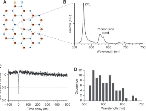
Despite the wide use as insulator for its high quality, pristine hBN is not free of impurities, defects, and dan-gling bonds. Several luminescence experiments have reported strong emission from a large variety of charge defects, impurities, and adatoms [97–99] that create pho-toactive states within the hBN band gap [100, 101]. Recent studies demonstrate that these defects can be associated to nitrogen vacancies (NVs), a carbon atom substituted to an N vacancy or oxygen impurities [100]. Moreover, Tran et al. have shown that NVs in hBN function as SPEs [96]. Figure 6A shows the typical atomic structure of hBN with an individual atomic defect. The spectrally resolved emis-sion of atomic defect at room temperature is shown in Figure 6B with the zero phonon line (ZPL) located around 575 nm and separated by ~ 50 nm from the first phonon side band.
Spectroscopy of SPEs is done in confocal configura-tion with a microscope objective of NA = 1 and a fiber-coupled spectrometer. In detection, the excitation laser at 532 nm is filtered out with a polarized beam splitter and long pass filter. Second-order correlation measure-ment shows good anti-bunching, unveiling the single photon nature of these emitters. An example is reported in Figure 6C where the coincidence counts are recorded using a Hanbury Brown and Twiss setup with continuous wave excitation. At zero delay time, the counts go below
0.5 (g2(0) = 0.24), confirming the single photon emission.
Power-dependent measurements revealed a three-level system with a metastable state. Moreover, these emitters are found to be stable over time and show high emission rate up to 4 million counts per second [102]. Time-depend-ent measuremTime-depend-ents indicate a lifetime around 2 ns.
Interestingly, experiments report different spectral shape for quantum emitters in hBN with the ZPL energy spanning over a large band, from the UV up to 750 nm [96, 103]. Figure 6D shows the spectral distribution of the ZPL emission energy of almost 90 emitters in our experiments.
Although individual emitters show different spectral shapes, the constant energy separation between the ZPL and the phonon side bands of ~ 160 meV suggests similar crystal structures [96]. It is also interesting to notice the correlation between the energy of the ZPL and the spectral shape. Recent studies suggest the presence of at least two families of quantum emitters in hBN with different life-time and brightness [22].
An interesting aspect is the spectral distribution among the same family of emitter. Within the same family, the ZPL can span over the 300-meV band. The cause of this large distribution has been tentatively attributed to local strain fluctuations of the hBN flakes. Electronic dis-order is induced in monolayer graphene by random strain
fluctuation due to the exfoliation process or the inhomo-geneous adhesion to the substrate [104]. Similarly, in hBN, strain can result in the displacement of the lattice atoms and the shifting of the energy levels of atomic-like defects. It has been calculated that strain in the range of − 5% to 5% can cause an energy shift of almost 200 meV, in agree-ment with the experiagree-mental observation.
The role of strain in the energy of the single photon emission can open interesting possibilities for the local tuning of the ZPL with applications in quantum comput-ing and quantum information where indistcomput-inguishability is of utmost importance.
5 Outlook
Heterogeneous integration of 2D materials with nano-photonics promises a new architecture of optoelectronic devices and quantum photonics. In addition to E-O modu-lators and photodetectors based on graphene, a variety of combinations of 2D materials including TMDCs [90], BP [7, 17, 105], hBN, and superconducting 2D niobium
disele-nide (NbSe2) [106] could further provide on-chip devices
including all-optical modulators [107], mode-locked ultra-fast laser [108], thermo-optic modulators [109], light-emit-ting diodes [110], and single photon sources [22].
Continued improvement in material and device fabrication is needed to facilitate the technology tran-sition into applications. There has been significant progress in epitaxial, large-scale, and high-yield trans-fer processes for certain materials including graphene
[14, 111, 112] and MoS2 [113, 114]; on the other hand, the
development of large-scale epitaxial hBN [115, 116] and other TMDCs continually advances. These developments could soon provide a hybrid platform that heterogene-ously integrates 2D materials with silicon CMOS techno-logy. To further ensure high-quality electronics and photonics based on 2D materials, suitable substrates and surface passivation are essential to ensure high-quality 2D devices. In addition, high-high-quality electrical contacts are also important to reduce contact resist-ance, improving device speed and power consumption. One-dimensional contacts to the hBN-encapsulated gra-phene [45] and graphite-gragra-phene contacts [117] show great promise. Work continues on scaling up these pro-cesses and extending low-resistivity contacts to other 2D materials.
The outstanding optical and electronic properties of 2D materials offer a level of control, heterogeneous material properties, and design flexibilities that are probably unprecedented in optoelectronics. Here, we reviewed a subset of applications: optical interconnect
550 A B C D 550 –100 0.0 0.5 1.0 0 100 200 Time delay (ns) Coincidence count s 300 400 500 0 2 4 6 8 10 12 Occurenc e 600 650 Wavelength (nm) 700 600 ZPL B N Phonon side band 650 Counts (a.u.) Wavelength (nm) 700 750
Figure 6: (A) Schematic of the atomic structure of hexagonal boron nitride. The dashed circle shows the structure of an NV in which one N atom is vacant and an adjacent B atom is substituted with N. (B) Typical room temperature spectrum of an SPE associated to an atomic-like defect. (C) Autocorrelation function (g2(τ)) showing anti-bunching at zero time delay. The histogram is measured using a Hanbury Brown and
Twiss setup with continuous wave excitation at 532 nm. (D) Spectral distribution of the ZPL emission for almost 90 individual emitters. The emission energy spans over the 150-nm range.
technologies including high-speed photodetectors [15, 16, 39] and modulators [10, 13], as well as device concepts for photonic quantum information processing, includ-ing progress toward efficient sinclud-ingle photon sources and single photon detectors. With the exceptional progress of the past decade, such a scalable 2D nanophotonic architecture could bring remarkable impacts for these applications in the near future, while promising other directions including back-end deposited silicon photon-ics [118], mid-infrared photonphoton-ics [119], THz detection [120, 121] and modulation [122], and also flexible pho-tonics [123].
Acknowledgments: G.G. acknowledges support by the
Swiss National Science Foundation. Measurements were supported in part by the National Science Foundation EFRI 2-DARE, award abstract no. 1542863, and in part by the Center for Excitonics, an Energy Frontier Research Center funded by the U.S. Department of Energy, Office of Science, Office of Basic Energy Sciences under award no. DE-SC0001088. C.P. was supported in part by the Stata Family Presidential Fellowship of Massachusetts Institute of Technology. R.-J.S. was supported in part by the Center for Excitonics, an Energy Frontier Research Center funded by the U.S. Department of Energy, Office of Science, Office of Basic Energy Sciences under award no. DE- SC0001088. K.C.F. acknowledges support from the Internal Research and Development in Raytheon BBN Technologies in pre-paring this manuscript.
References
[1] Miller DAB. Device requirements for optical interconnects to silicon chips. Proc IEEE 2009;97:1166–85.
[2] Bergman K, Carloni LP, Biberman A, Chan J, Hendry G. Photonic Network-on-Chip Design. Springer, New York, 2014.
[3] Hochberg M, Baehr-Jones T. Towards fabless silicon photonics. Nat Photonics 2010;4:492–4.
[4] Liu K. Review and perspective on ultrafast wavelength-size electro-optic modulators. Laser Photonics Rev 2015;9:172–94. [5] Heck MJR, Bauters JF, Davenport ML, et al. Hybrid silicon
pho-tonic integrated circuit technology. IEEE J Sel Top Quant Electron 2013;19:6100117.
[6] Liu Y, Ran Ye C, Khan S, Sorger VJ. Van der Waals heterostruc-tures and devices. Nat Rev Mater 2016;1:16042.
[7] Xia F, Wang H, Xiao D, Dubey M, Ramasubramaniam A. Two-dimensional material nanophotonics. Nat Photonics 2014;8:899–907.
[8] Liu M, Yin X, Ulin-Avila E, et al. A graphene-based broadband optical modulator. Nature 2011;474:64–7.
[9] Liu M, Yin X, Zhang X. Double-layer graphene optical modulator. Nano Lett 2012;12:1482–5.
[10] Gao Y, Shiue RJ, Gan X, et al. High-speed electro-optic modula-tor integrated with graphene-boron nitride heterostructure and photonic crystal nanocavity. Nano Lett 2015;15:2001–5. [11] Qiu C, Gao W, Vajtai R, et al. Efficient modulation of 1.55 μm
radiation with gated graphene on a silicon microring resonator. Nano Lett 2014;14:6811–5.
[12] Ding Y, Zhu X, Xiao S, et al. Effective electro-optical modula-tion with high extincmodula-tion ratio by a graphene-silicon microring resonator. Nano Lett 2015;15:4393–400.
[13] Phare CT, Daniel Lee Y-H, Cardenas J, Lipson M. Graphene electro-optic modulator with 30 GHz bandwidth. Nat Photonics 2015;9:511–4.
[14] Schall D, Neumaier D, Mohsin M, et al. 50 GBit/s photodetec-tors based on wafer-scale graphene for integrated silicon pho-tonic communication systems. ACS Phopho-tonics 2014;1:781–4. [15] Shiue RJ, Gao Y, Wang Y, et al. High-responsivity
graphene-boron nitride photodetector and autocorrelator in a silicon photonic integrated circuit. Nano Lett 2015;15:7288–93. [16] Gan X, Shiue R-J, Gao Y, et al. Chip-integrated ultrafast
gra-phene photodetector with high responsivity. Nat Photonics 2013;7:883–7.
[17] Youngblood N, Chen C, Koester SJ, Li M. Waveguide-integrated black phosphorus photodetector with high responsivity and low dark current. Nat Photonics 2015;9:247–52.
[18] Gan X, Gao Y, Mak KF, et al. Controlling the spontaneous emis-sion rate of monolayer MoS2 in a photonic crystal nanocavity.
Appl Phys Lett 2013;103:181119.
[19] Wu S, Buckley S, Schaibley JR, et al. Monolayer semicon-ductor nanocavity lasers with ultralow thresholds. Nature 2015;520:69–72.
[20] Ye Y, Wong ZJ, Lu X, et al. Monolayer excitonic laser. Nat Pho-tonics 2015;9:733–7.
[21] Fong KC, Schwab KC. Ultrasensitive and wide-bandwidth ther-mal measurements of graphene at low temperatures. Phys Rev X 2012;2:031006.
[22] Tran TT, Elbadawi C, Totonjian D, et al. Robust multicolor single photon emission from point defects in hexagonal boron nitride. ACS Nano 2016;10:7331–8.
[23] Koperski M, Nogajewski K, Arora A, et al. Single photon emitters in exfoliated WSe2 structures. Nat Nanotechnol 2015;10:503–6.
[24] He YM, Clark G, Schaibley JR, et al. Single quantum emitters in monolayer semiconductors. Nat Nanotechnol 2015;10:497–502.
[25] Gan X, Mak KF, Gao Y, et al. Strong enhancement of light-matter interaction in graphene coupled to a photonic crystal nanocav-ity. Nano Lett 2012;12:5626.
[26] Gan X, Shiue RJ, Gao Y, et al. Controlled light-matter interac-tion in graphene electrooptic devices using nanophotonic cavities and waveguides. IEEE J Sel Top Quant Electron 2014;20:95–105.
[27] Dean CR, Young AF, Meric I, et al. Boron nitride substrates for high-quality graphene electronics. Nat Nanotechnol 2010;5:722–6. [28] Mak KF, Sfeir MY, Wu Y, et al. Measurement of the optical
con-ductivity of graphene. Phys Rev Lett 2008;101:196405. [29] Kravets VG, Grigorenko AN, Nair RR, et al. Spectroscopic
ellipsometry of graphene and an exciton-shifted van Hove peak in absorption. Phys Rev B Condens Matter Mater Phys 2010;81:155413.
[30] Wu S, Buckley S, Jones A, et al. Control of two-dimensional exci-tonic light emission via phoexci-tonic crystal. 2D Mater 2014;1:011001.
[31] Splendiani A, Sun L, Zhang Y, et al. Emerging photolumines-cence in monolayer MoS2. Nano Lett 2010;10:1271–5.
[32] Mak KF, Lee C, Hone J, et al. Atomically thin MoS2: a new
direct-gap semiconductor. Phys Rev Lett 2010;105:136805. [33] Schwagmann A, Kalliakos S, Ellis D, et al. In-plane
single-photon emission from a L3 cavity coupled to a single-photonic crystal waveguide. Opt Express 2012;20:28614.
[34] Chalcraft A, Lam S, O’Brien D, et al. Mode structure of the L3 photonic crystal cavity. Appl Phys Lett 2007;90:241117. [35] Salehzadeh O, Djavid M, Tran NH, Shih I, Mi Z. Optically
pumped two-dimensional MoS2 lasers operating at
room-tem-perature. Nano Lett 2015;15:5302–6.
[36] Liu X, Galfsky T, Sun Z, et al. Strong light–matter coupling in two-dimensional atomic crystals. Nat. Photonics 2014;9:30–4.
[37] Li H, Anugrah Y, Koester SJ, Li M. Optical absorption in graphene integrated on silicon waveguides. Appl Phys Lett 2012;101:2–7.
[38] Lu Z, Zhao W. Nanoscale electro-optic modulators based on graphene-slot waveguides. J Opt Soc Am B 2012;29:1490. [39] Wang J, Cheng Z, Chen Z, et al. High-responsivity
graphene-on-silicon slot waveguide photodetectors. Nanoscale 2016;8:13206–11.
[40] Wang F, Zhang Y, Tian C, et al. Gate-variable optical transitions in graphene. Science 2008;320:206–9.
[41] Li ZQ, Henriksen EA, Jiang Z, et al. Dirac charge dynamics in graphene by infrared spectroscopy. Nat Phys 2008;4:532–5. [42] Mohsin M, Schall D, Otto M, et al. Graphene based low
inser-tion loss electro-absorpinser-tion modulator on SOI waveguide. Opt Express 2014;22:15292.
[43] Gan X, Shiue R-J, Gao Y, et al. High-contrast electrooptic modu-lation of a photonic crystal nanocavity by electrical gating of graphene. Nano Lett 2013;13:691–6.
[44] Dasgupta S, Stoesser G, Schweikert N, et al. Printed and elec-trochemically gated, high-mobility, inorganic oxide nanopar-ticle FETs and their suitability for high-frequency applications. Adv Funct Mater 2012;22:4909–19.
[45] Wang L, Meric I, Huang PY, et al. One-dimensional electrical contact to a two-dimensional material. Science 2013;342:614–7. [46] Lee GHH, Yu Y-J, Lee C, et al. Electron tunneling through atomi-cally flat and ultrathin hexagonal boron nitride. Appl Phys Lett 2011;99:1–4.
[47] Voskoboynikov VV, Gritsenko VA, Efimov VM, Lesnikovskaya VE, Edelman FL. Structure and electrophysical properties of boron nitride thin films. Phys Status Solidi 1976;34:85–94. [48] Manipatruni S, Dokania RK, Schmidt B, et al. Wide
tempera-ture range operation of micrometer-scale silicon electro-optic modulators. Opt Lett 2008;33:2185–7.
[49] Teng J, Dumon P, Bogaerts W, et al. Athermal silicon-on-insulator ring resonators by overlaying a polymer cladding on narrowed waveguides. Opt Express 2009;17:14627–33. [50] Reed GT, Mashanovich G, Gardes FY, Thomson DJ. Silicon
opti-cal modulators. Nat Photonics 2010;4:518–26.
[51] Youngblood N, Anugrah Y, Ma R, Koester SJ, Li M. Multifunc-tional graphene optical modulator and photodetector inte-grated on silicon waveguides. Nano Lett 2014;14:2741–6. [52] Wang J, Lee S. Ge-photodetectors for Si-based optoelectronic
integration. Sensors 2011;11:696–718.
[53] Liang D, Roelkens G, Baets R, Bowers JE. Hybrid integrated platforms for silicon photonics. Materials 2010;3:1782–1802.
[54] Atabaki AH, Meng H, Alloatti L, Mehta KK, Ram RJ. High-speed polysilicon CMOS photodetector for telecom and datacom. Appl Phys Lett 2016;109:111106.
[55] Mueller T, Xia F, Avouris P. Graphene photodetectors for high-speed optical communications. Nat Photonics 2010;4:297–301. [56] Freitag M, Freitag M, Low T, Xia F, Avouris P. Photoconductivity
of biased graphene. Nat Photonics 2012;7:53–9.
[57] Brida D, Tomadin A, Manzoni C, et al. Ultrafast collinear scat-tering and carrier multiplication in graphene. Nat Commun 2013;4:1987.
[58] Tielrooij KJ, Song JCW, Jensen SA, et al. Photoexcitation cas-cade and multiple hot-carrier generation in graphene. Nat Phys 2013;9:248–52.
[59] Özyilmaz B, Jarillo-Herrero P, Efetov D, Abanin DA, Levitov LS, Kim P. Electronic transport and quantum hall effect in bipolar graphene p-n-p junctions. Phys Rev Lett 2007;99:166804. [60] Özyilmaz B, Jarillo-Herrero P, Efetov D, et al. Electronic
trans-port in locally gated graphene nanoconstrictions. Appl. Phys. Lett. 2007;91:192107.
[61] Pospischil A, Humer M, Furchi MM, et al. CMOS-compatible graphene photodetector covering all optical communication bands. Nat Photonics 2013;7:892–6.
[62] Lu C, Fu Q, Huang S, Liu J. Polymer electrolyte-gated carbon nanotube field-effect transistor. Nano Lett 2004;4:623–7. [63] Efetov DK, Maher P, Glinskis S, Kim P. Multiband transport in
bilayer graphene at high carrier densities. Phys Rev B Condens Matter 2011;84:161412.
[64] Efetov DK, Kim P. Controlling electron-phonon interactions in graphene at ultrahigh carrier densities. Phys Rev Lett 2010;105:256805.
[65] Guo Y, Smith RB, Yu Z, et al. Li intercalation into graphite: direct optical imaging and Cahn-Hilliard reaction dynamics. J Phys Chem Lett 2016;7:2151–6.
[66] Song JCW, Rudner MS, Marcus CM, Levitov LS. Hot carrier transport and photocurrent response in graphene. Nano Lett 2011;11:4688–92.
[67] Gabor NM, Song JCW, Ma Q, et al. Hot carrier-assisted intrinsic photoresponse in graphene. Science 2011;334:648–52. [68] Wang X, Cheng Z, Xu K, Tsang HK, Xu J-B. High-responsivity
graphene/silicon-heterostructure waveguide photodetectors. Nat Photonics 2013;7:888–91.
[69] Guo Q, Pospischil A, Bhuiyan M, et al. Black phosphorus mid-infrared photodetectors with high gain. Nano Lett 2016;16:4648–55.
[70] Graham MW, Shi S-F, Ralph DC, Park J, McEuen PL. Photocur-rent measurements of supercollision cooling in graphene. Nat Phys 2012;9:103–8.
[71] Liang T, Tsang H, Day I, et al. Silicon waveguide two-photon absorption detector at 1.5 μm wavelength for autocorrelation measurements. Appl Phys Lett 2002;81:1323.
[72] Hayat A, Nevet A, Ginzburg P, et al. Applications of two-photon processes in semiconductor photonic devices: invited review. Semicond Sci Technol 2011;26:083001.
[73] Duchesne D, Razzari L, Halloran L, et al. Two-photon detection in a MQW GaAs Laser at 1.55μm. In: Conference on Lasers and Electro-Optics/International Quantum Electronics Conference, p. IMH5, OSA, Washington, DC, 2009.
[74] Tielrooij KJ, Piatkowski L, Massicotte M, et al. Generation of photovoltage in graphene on a femtosecond timescale through efficient carrier heating. Nat Nanotechnol 2015;10:437–43.
[75] Balandin AA. Thermal properties of graphene and nanostruc-tured carbon materials. Nat Mater 2011;10:569–81.
[76] Balandin AA, Ghosh S, Bao W, et al. Superior thermal conduc-tivity of single-layer graphene. Nano Lett 2008;8:902–7. [77] Fong KC, Schwab KC. Publisher’s note: ultrasensitive and
wide-bandwidth thermal measurements of graphene at low temperatures. Phys Rev X 2012;2:031006.
[78] Fong KC, Wollman EE, Ravi H, et al. Measurement of the electronic thermal conductance channels and heat capacity of graphene at low temperature. Phys Rev X 2013;3:041008. [79] Zuev YM, Chang W, Kim P. Thermoelectric and
magnetothermo-electric transport measurements of graphene. Phys Rev Lett 2009;102:096807.
[80] McKitterick CB, Prober DE, Karasik BS. Performance of graphene thermal photon detectors. J Appl Phys 2013;113:044512.
[81] Wei J, Olaya D, Karasik BS, Pereverzev SV, Sergeev AV, Ger-shenson ME. Ultrasensitive hot-electron nanobolometers for terahertz astrophysics. Nat Nanotechnol 2008;3:496–500. [82] Yan J, Kim M-H, Elle JA, et al. Dual-gated bilayer graphene
hot-electron bolometer. Nat Nanotechnol 2012;7:472–8.
[83] Karasik BS, Pereverzev SV, Soibel A, et al. Energy-resolved detec-tion of single infrared photons with λ = 8 μm using a supercon-ducting microbolometer. Appl Phys Lett 2012;101:052601. [84] Crossno J, Shi JK, Wang K, et al. Observation of the Dirac fluid
and the breakdown of the Wiedemann-Franz law in graphene. Science 2016;351:1058–61.
[85] Efetov DK, Wang L, Handschin C, et al. Specular interband Andreev reflections at van der Waals interfaces between gra-phene and NbSe2. Nat Phys 2015;12:328–32.
[86] Wan Z, Kazakov A, Manfra M, et al. Induced superconductiv-ity in high-mobilsuperconductiv-ity two-dimensional electron gas in gallium arsenide heterostructures. Nat. Commun. 2015;6:7426. [87] Efetov DK, Efetov KB. Crossover from retro to specular Andreev
reflections in bilayer graphene. Phys Rev B Condens Matter 2016;94:075403.
[88] Kimble HJ. The quantum internet. Nature 2008;453:1023–30. [89] Knill E, Laflamme R, Milburn GJ. A scheme for efficient quantum
computation with linear optics. Nature 2001;409:4652. [90] Mak KF, Shan J. Photonics and optoelectronics of 2D
semi-conductor transition metal dichalcogenides. Nat Photonics 2016;10:216–26.
[91] Chakraborty C, Kinnischtzke L, Goodfellow KM, Beams R, Vami-vakas AN. Voltage-controlled quantum light from an atomically thin semiconductor. Nat Nanotechnol 2015;10:507–11. [92] Srivastava A, Sidler M, Allain AV, Lembke DS, Kis A, Imamoğlu
A. Optically active quantum dots in monolayer WSe2. Nat
Nano-technol 2015;10:491–6.
[93] Kumar S, Brotóns-Gisbert M, Al-Khuzheyri R, et al. Resonant laser spectroscopy of localized excitons in monolayer WSe2.
Optica 2016;3:882–6.
[94] Bayer M, Ortner G, Stern O, et al. Fine structure of neutral and charged excitons in self-assembled In(Ga)As/(Al)GaAs quan-tum dots. Phys Rev B Condens Matter 2002;65:195315. [95] Caldwell JD, Kretinin AV, Chen Y, et al. Sub-diffractional
volume-confined polaritons in the natural hyperbolic material hexago-nal boron nitride. Nat Commun 2014;5:5221.
[96] Tran TT, Bray K, Ford MJ, Toth M, Aharonovich I. Quantum emis-sion from hexagonal boron nitride monolayers. Nat Nanotech-nol 2015;11:37–41.
[97] Zunger A, Katzir A. Point defects in hexagonal boron nitride: II. Theoretical studies. Phys Rev B Condens Matter 1975;11:2378–90.
[98] Andrei EY, Katzir A, Suss JT. Point defects in hexagonal boron nitride: III. EPR in electron-irradiated BN. Phys Rev B Condens Matter 1976;13:2831–4.
[99] Garcia AGF, Neumann M, Amet F, et al. Effective cleaning of hexagonal boron nitride for graphene devices. Nano Lett 2012;12:4449–54.
[100] Wong D, Velasco J. Jr, Ju L, et al. Characterization and manipu-lation of individual defects in insulating hexagonal boron nitride using scanning tunnelling microscopy. Nat Nanotech-nol 2015;10:949–53.
[101] Remes Z, Nesladek M, Haenen K, Watanabe K, Taniguchi T. The optical absorption and photoconductivity spectra of hexagonal boron nitride single crystals. Phys Stat Sol A 2005;202:2229–33.
[102] Martínez LJ, Pelini T, Waselowski V, et al. Efficient single photon emission from a high-purity hexagonal boron nitride crystal. Phys Rev B Condens Matter 2016;94:121405. [103] Bourrellier R, Meuret S, Tararan A, et al. Bright UV
sin-gle photon emission at point defects in h-BN. Nano Lett 2016;16:4317–21.
[104] Couto NJG, Costanzo D, Engels S. Random strain fluctuations as dominant disorder source for high-quality on-substrate graphene devices. Phys Rev X 2014;4:041019.
[105] Li L, Yu Y, Ye GJ, et al. Black phosphorus field-effect transis-tors. Nat Nanotechnol 2014;9:372–7.
[106] Ugeda MM, Bradley AJ, Zhang Y, et al. Characterization of collective ground states in single-layer NbSe2. Nat Phys
2015;12:92–7.
[107] Li W, Chen B, Meng C, et al. Ultrafast all-optical graphene modulator. Nano Lett 2014;14:955–9.
[108] Sun Z, Hasan T, Torrisi F, et al. Graphene mode-locked ultra-fast laser. ACS Nano 2010;4:803–10.
[109] Gan S, Cheng C, Zhan Y, et al. A highly efficient thermo-optic microring modulator assisted by graphene. Nanoscale 2015;4:163–4.
[110] Withers F, Del Pozo-Zamudio O, Mishchenko A, et al. Light-emitting diodes by band-structure engineering in van der Waals heterostructures. Nat Mater 2015;14:301–6.
[111] Lin Y-M, Valdes-Garcia A, Han S-J, et al. Wafer-scale graphene integrated circuit. Science 2011;332:1294–7.
[112] Gao L, Ni G-X, Liu Y, Liu B, Castro Neto AH, Loh KP. Face-to-face transfer of wafer-scale graphene films. Nature 2013;505:190–4.
[113] Wang H, Yu L, Lee Y-H, et al. Integrated circuits based on bilayer MoS2 transistors. Nano Lett 2012;12:4674–80.
[114] Yu L, Lee YH, Ling X, et al. Graphene/MoS2 hybrid
technol-ogy for large-scale two-dimensional electronics. Nano Lett 2014;14:3055–63.
[115] Kim SM, Hsu A, Park MH, et al. Synthesis of large-area multi-layer hexagonal boron nitride for high material performance. Nat Commun 2015;6:8662.
[116] Jang A-R, Hong S, Hyun C, et al. Wafer-scale and wrinkle-free epitaxial growth of single-orientated multilayer hexagonal boron nitride on sapphire. Nano Lett 2016;16:3360–6. [117] Chari T, Ribeiro-Palau R, Dean CR, Shepard K. Resistivity
of rotated graphite-graphene contacts. Nano Lett 2016;16:4477–82.
[118] Lee YHD, Lipson M. Back-end deposited silicon photonics for monolithic integration on CMOS. IEEE J Sel Top Quantum Electron 2013;19:8200207.
[119] Shankar R, Leijssen R, Bulu I, Lončar M. Mid-infrared photonic crystal cavities in silicon. Opt Express 2011;19:5579.
[120] Vicarelli L, Vitiello MS, Coquillat D, et al. Graphene field-effect transistors as room-temperature terahertz detectors. Nat Mater 2012;11:865–71.
[121] Cai X, Sushkov AB, Suess RJ, et al. Sensitive room-tempera-ture terahertz detection via the photothermoelectric effect in graphene. Nat Nanotechnol 2014;9:814–9.
[122] Gao W, Shu J, Reichel K, et al. High-contrast terahertz wave modulation by gated graphene enhanced by extraordinary trans-mission through ring apertures. Nano Lett 2014;14:1242–8. [123] Li L, Lin H, Qiao S, et al. Integrated flexible chalcogenide
![Figure 3A sketches a waveguide-coupled graphene photodetector [15] fabricated on a CMOS-compatible PIC](https://thumb-eu.123doks.com/thumbv2/123doknet/13842351.444051/6.892.187.689.104.415/figure-sketches-waveguide-coupled-graphene-photodetector-fabricated-compatible.webp)
![Figure 5: (A) Schematics of a graphene bolometer circuit [21, 78]. Due to its exceedingly small electronic heat capacity, the graphene sheet acts as an ultrasensitive heat absorber](https://thumb-eu.123doks.com/thumbv2/123doknet/13842351.444051/9.892.108.806.98.443/schematics-graphene-bolometer-exceedingly-electronic-capacity-graphene-ultrasensitive.webp)