The Development of a Prototype
Zone-Plate-Array Lithography (ZPAL) System
by
Amil Ashok Patel
B.S., Electrical Engineering (2002)
Duke University
Submitted to the
Department of Electrical Engineering and Computer Science
in partial fulfillment of the requirements for the degree of
Master of Science
at the
MASSACHUSETTS INSTITUTE OF TECHNOLOGY
May 2004
Luvit 2-G47
@
Massachusetts Institute of Technology 2004. All rights reserved.
A u th or ...
...
Department of Electrical Engineering and Computer Science
.May Q7, 2004
Certified by...
...
7
Henry I.
Smith
Keithley Professor of EECS
_ j-iIThesis Supervisor
Accepted by
Arthrf' C. Smith
Chairman, Department Committee on Graduate Students
MASSACHUSETTS INST E OF TECHNOLOGY
The Development of a Prototype Zone-Plate-Array
Lithography (ZPAL) System
by
Amil Ashok Patel
Submitted to the Department of Electrical Engineering and Computer Science on May 07, 2004, in partial fulfillment of the
requirements for the degree of Master of Science
Abstract
The research presented in this paper aims to build a Zone-Plate-Array Lithography (ZPAL) prototype tool that will demonstrate the high-resolution, parallel pattern-ing capabilities of the architecture. The experiment will require the integration of micromechanical spatial light modulators with an existing zone-plate-array testbed lithography tool. The system development requires an efficient data-delivery system to promote throughput and a thoughtful optical channel to optimize the lithographic performance of zone-plates. Lithography results obtained from the prototype will be presented along with basic performance characteristics.
Thesis Supervisor: Henry I. Smith Title: Keithley Professor of EECS
Acknowledgments
In the journey of life we create a unique story for which history remembers us. Part of the joy of life comes from sharing our stories to teach a lesson or to incite a laugh. I feel priviledged to know that so many of my stories will begin with the phrase "Back
in my days at M.I.T...".
At the foundation of these stories will be the inspiration, Professor Henry Smith. He has given me a great opportunity work on a truly revolutionary project with remarkable people. Under his tutelage I have learned that paving a new path can be difficult and frustrating, but it comes with a true sense of accomplishment.
I also appreciate the insights I have received from Professor George Barbastathis
on all things optics and all things Greek. All of the optical engineering required for this project was made possible by 2.710.
Thank you to my colleauges at the NSL for their wealth of knowledge and collab-orative spirit. The idea of passing down knowledge (stories of triumph and failure) between the generations is nowhere more apparent than in this community of schol-ars. It is the key to the progress made in the laboratory every day. Thank you also to Jim Daley, Jimmy Carter, and Cindy Lewis for keeping the laboratory and office running reliably and safely.
No great lab can exist without the leadership of individuals who go above and beyond to guide, challenge and communicate. In my time as a ZPAL project member, Rajesh Menon has served as a great mentor. I have learned a great deal from him on what kind of initiative it takes to be a successful researcher. I can only hope to elevate my standards to his level.
There is also my first officemate, Feng Zhang. He was quick to make me feel at home in the group and help me with the problems I have faced inside the classroom and laboratory. He is someone I consider a true engineer (he can solder and he has a fundamental understanding for how things work... be it a diffraction grating or an automobile).
Thanks also to Officmate Version 2.0, Dave Chao, for making ZPAL a more
citing venture. Beyond my labmates there are a large number of friends at MIT to thank. They impacted me through their lunch-time wisdom and through discussions at the gym.
Additional thanks to Dario Gil and David Carter for creating the foundation for the ZPAL project and assisting me even after breaking free of the corridors of MIT.
Finally, thank you to my family and friends for the support throughout. It is their enthusiasm and curiosity for my work that makes working this hard worthwhile.
Contents
1 Introduction
1.1 The Lithography Landscape . . . .
1.1.1 Key Challenges to OPL . . . . 1.1.2 E-beam Lithography . . . . 1.1.3 Building for an Unaddressed Niche . . . .
1.2 Zone-Plate-Array Lithography . . . . 1.2.1 Zone-Plate Description . . . . 1.2.2 Micromechanics . . . .
1.2.3 The ZPAL Test-bed . . . .
1.2.4 Evolution from ZPAL Test-bed to ZPAL Prototype . . . .
2 The Data-Delivery System
2.1 Scale of the Data-Delivery Problem . . . . 2.2 The ZPAL Data-Delivery Prototype Requirements . . . .
2.2.1 GLV Algorithm . . . . 2.3 Hardware Architecture . . . . 2.4 Software Architecture . . . . 2.4.1 Validate Functionality of Hardware . . . . 2.4.2 Architecture to Improve Real-time Throughput . . . .
2.4.3 Front-end Software . . . .
3 Design and Test of the Projection Optics
3.1 Projection Optics Requirement . . . .
7 15 15 16 17 17 18 18 22 23 27 29 29 30 31 32 35 35 39 42 47 47
3.2 The Optical Operation of the Grating Light Valve . . . . 48
3.2.1 Physical Description of GLV . . . . 48
3.2.2 M athematical M odel of the GLV . . . . 50
3.3 Single Lens Imaging System . . . . 53
3.4 Projection Optics . . . . 55 3.4.1 The 4-F System . . . . 56 3.4.2 Filter Design . . . . 58 3.4.3 Lens Design . . . . 58 3.5 Alignment . . . . 61 4 Lithography Results 65 4.1 Experimental Background . . . . 65 4.2 Results . . . . 66
4.2.1 Parallel Patterning with Zone Plates . . . . 66
4.2.2 Resolution . . . . 66
4.2.3 Field Stitching . . . . 69
4.2.4 Process Latitude . . . . 69
4.3 Conclusion . . . . 71
List of Figures
1-1 Closeup depiction of the ZPAL tool. The spatial-light-modulators(not shown) are responsible for modulating the individual beams to the zone-plates. The beams are focused by the zone-plates. Having more zone-plates writing in parallel means higher throughput. . . . . 19
1-2 Cross-sectional view of an amplitude zone-plate. The optical path of the radiation is traced to the first-order focus. It is important to note that the focussing effect comes from diffraction rather than refraction 20
1-3 (Left)Figure depicting the focal points associated with the +1, -1, +3, -3 diffracted orders. The +1 is used for lithography. (Right)Simulated
point-spread function for a NA=0.85 zone-plate operating with a source of A = 400nm . . . . . 21
1-4 (Top) Drawing of a single GLV pixel. (Bottom) Simple one-to-one mapping of GLV pixels to zone-plates. . . . . 23 1-5 The zone-plate test-bed architecture. This scheme does not address
the multiplexing nature of the ZPAL concept. A single SLM is used rather than an array of micromechanical SLMs. By making the beam broad, the light from a single SLM can illuminate an entire array of zone-plates. . . . . 24
1-6 A zone-plate array was fabricated to demonstrate the effectiveness of
having many zone-plates writing in parallel. The array shown contains
1000 zone-plates and was written with e-beam lithography using HSQ
negative resist . . . . 25
1-7 Patterning result of dense lines and spaces by the ZPAL test-bed demonstrating k, of 0.32 which is on the frontier of lithographic per-form ance . . . . 26 1-8 Schematic of the ZPAL prototype architecture including all four
pri-m ary elepri-m ents. . . . . 27
2-1 Schematic demonstrating how the CPU and the NI cards were config-ured and interfaced to the GLV. . . . . 33
2-2 Timing diagram capturing the data uploading algorithm. . . . . 34
2-3 A block diagram of the data-delivery architecture created in the first
iteration. The entire process is conducted in real-time. . . . . 35
2-4 Optical setup for testing functionality and throughput of the data-delivery system. When data for any GLV element is 0, no light goes into the 1st order. However, if the data is 255, then light is modulated into the 1st diffracted order which can be detected by a photodiode. 36 2-5 This figure charts the modulation of the GLV as observed by a
photo-detector. One period on the graph corresponds to sending two data frames to the GLV. One to set all pixels to 255 and a second to set all pixels to 0. The data rate shown is approximately 1 Gbps. Note that this data throughput is the peak data throughput. . . . . 37 2-6 (Left) Plots the time required to generate and output increasing
num-ber of frames for the first generation software architecture. The com-plexity of the operation is 0(n 2
). (Right) Plots the system throughput
with respect to the number of frames. The real-time throughput is significantly below that required for a maskless lithography tool. [12] 38 2-7 A block diagram of the data-delivery architecture created in the second
software iteration. The innovation in this architecture is the idea of breaking up the process into offline and real-time components. . . . 39
2-8 (Left) Plots the time required to send increasing number of frames for the second generation software architecture. The algorithm demon-strates a linear progression which rather than an exponential one. This is critical as the number of frames going through the system exceeds one million. (Right) Plots the system throughput with respect to the num ber of fram es. . . . . 40
2-9 (Left) Compares the cycle delay with the two different data-delivery architectures explored. (Right) Plots the real-time system throughput 41 2-10 (Left) An arbitrary field is shown along with its pixels and their
se-quencing. (Right) A set of three arbitrary frames. For a system using
the GLV, N < 1088 . . . . 45
3-1 A cartoon of a single GLV cell. . . . . 48
3-2 The profile view of the GLV. (Left) No voltage is applied between
the ribbons and the substrate resulting in a simple mirror. (Right) A voltage is applied such that 6 = A/4. Light is modulated into diffracted orders. ... ... 49
3-3 Interpretation of Equation 3.2. There are two amplitude gratings su-perimposed upon each other. Transparent regions are assumed to in-troduce no loss. ... ... 50
3-4 The intensity spectrum for a phase grating when the L = A/2 or 6 =
A/4. Note that there is no zero order. . . . . 52 3-5 Observation of how energy is transferred from 1st order to Oth order
as the deflection distance of the ribbons is altered. . . . . 53 3-6 The basic imaging system used to test the functionality of the GLV.
When data is uploaded into the GLV, the result can be observed on a computer monitor. The object and image obey the Lens Law . . . . 54
3-7 Images of the GLV captured on camera. (Top) Single GLV pixels resolved. One pixel is on and the next three are off. (Middle) Periodic image created by four pixels on and four pixels off. (Bottom) Four
pixels on and 12 pixels off. . . . . 55
3-8 The 4-F is the optical channel used in the ZPAL prototype to map the GLV pixels to zone-plates. . . . . 56 3-9 Spectrum analysis of phase grating. When illuminating a zone-plate,
it is ideal to select only one spatial frequency. . . . . 59 3-10 The telephoto lens design used in the GLV imaging system . . . . 60 3-11 The optical imaging system used for alignment. The reflection from the
zone-plate array plane is captured on CCD and displayed to a monitor as real-time adjustments are made. . . . . 62
3-12 Images of the GLV illuminating individual zone plates. (Top)
Ev-ery other zone-plate in the array is illuminated. Each zone-plate is illuminated by four GLV pixels. (Bottom) Adjacent zone-plates are illum inated. . . . . 63
4-1 Micrographs showing four different patterns written simultaneously by four zone-plates. . . . . 67
4-2 Resolution demonstration of the ZPAL prototype. . . . . 68
4-3 An optical device that spans 17 zone-plate fields was fabricated with the prototype to demonstrate the parallel patterning capability in
ad-dition to field stitching. . . . . 70
4-4 A close view of the waveguide shown in Figure 4-3. The stitching error is below 50nm . . . . . 71
List of Tables
4.1 Experimental wafer recipe for ZPAL lithography. . . . . 65
Chapter 1
Introduction
Let me begin with an axiom from the field of economics; technological innovation increases the productivity of labor and allows society to achieve a higher standard of living. We are abound with new ideas for inventions that have the potential to make the world better off. The realization of these ideas can be hindered by fun-damental scientific barriers, by economic constraints or a combination of the two. In this research, our aim is to build a tool which takes advantage of emerging tech-nologies to topple current economic constraints and future physical constraints in the field of nanolithography. The presence of this tool will increase the productivity of nanotechnology innovators and lead to faster technological progress.
1.1
The Lithography Landscape
The ability to create patterns or structures in the nanometer domain is quite an awe-some power. Entropy in our macroscopic world is evident everywhere from traffic jams to bad hair days. However, through advanced lithography techniques we have the ability to create harmonious order in the "nano-world" (500nm and below). This formidable power to manufacture on the nano-scale is pushing the frontier in semicon-ductors (manipulation of electrons), photonics (manipulation of light), biotechnology (manipulation of cells and other organic materials) and nanotechnology (manipulation of molecules).
Research and Development in the fields mentioned above are characterized by myriad design iterations and low-volume production. Low-volume and low cost is an oxymoron in the lithography industry. The key challenge faced by tool makers in the nanolithography sector is taming the economic costs. On the surface, the cost is manifested in terms of high capital costs. Beyond monetary concerns, there is an opportunity cost of lost time for researchers and engineers that is measured in terms of long turn-around times1.
The two key lithography technologies in the industrial and research setting are Optical Projection Lithography (OPL) and E-beam lithography. OPL is the vogue technique used by the semiconductor industry to bring order to the nanoscale. The key features and drawbacks of these systems is discussed in the sections below.
1.1.1
Key Challenges to OPL
In the OPL paradigm, a pattern on a mask is projected onto a resist coated wafer with a 4x demagnification. The great benefit of OPL is its ability to reproduce patterns
with high-fidelity at high volumes.
The feature size for all optical lithography tools is characterized by Equation 1.1
Wmin = ki (1.1)
NA
As research begins to bridge "top-down" manufacturing (lithography) with "bottom-up" manufacturing (self-assembly), creating smaller features is critical. In the semi-conductor industry, smaller features has a spectrum of advantages from more cost-efficient manufacturing to improvements in circuit performance.
Looking back at Equation 1.1, to make smaller features we are forced to utilize shorter wavelengths of light A assuming k, and NA are fixed. However, refractive optics for radiation below A = 157 nm, the current industry standard, do not exist
because most materials are opaque in this region. This is a fundamental barrier to the continued evolution of OPL. Even materials used today, namely CaF2, are costly
1
to grow and form into lenses, which results in higher equipment costs.
The expensive optics add significant fixed cost to the tool. OPL systems operating at 193 nm cost around $25 million, which makes it particularly unattractive in an R&D setting. Beyond that, the inherent costs associated with masks must also be calculated. As we move to shorter wavelengths, the cost associated with masks begins to skyrocket. For the current 90 nm technology a mask set will cost more than $1 million, and it is projected that a mask set for the 65nm node due 2007 will cost
$3 million[19]. This amounts to exorbitant marginal costs since one must have a
custom mask fabricated for each unique design. The only way to recover the costs is to produce a large volume, a luxury enjoyed by few. Under this cost scheme, there is no room for error and no room to try risky ideas.
1.1.2
E-beam Lithography
E-beam lithography is a direct write tool which does away with the masks. The pattern is written directly using an electron beam as the pen. This system offers resolution surpassing that offered by OPL. However, e-beam suffers from dramatically slow write times. While this may be acceptable for small, high-resolution patterns, this type of tool cannot reach the throughput required by development related needs.
1.1.3
Building for an Unaddressed Niche
Where the advantageous characteristics of OPL and e-beam lithography converge exists a niche not currently recognized by tool makers. This void in the lithography tool market is characterized by maskless, high resolution, fast-writing speed, and low cost. When one says low cost, it signifies low tool cost, minimal marginal cost for new designs and short turn-around times. Such a niche is asking to be filled by the millions of current innovators and future innovators. The tool would increase the technology discovery process by bringing ideas to fruition effectively and efficiently. Alternative tools and methodologies must be pursued so that innovation is not crowded out by factors other than ingenuity, or the lack thereof.
1.2
Zone-Plate-Array Lithography
It is the hope of researchers in the NanoStructures Laboratory to address the short-comings of OPL and existing maskless lithography techniques with a radical scheme named Zone-Plate-Array Lithography (ZPAL). ZPAL was first proposed by Henry I. Smith in 1996 [21]. There are four key components to the ZPAL architecture:
1. A radiation source
2. A Spatial Light Modulator
3. An array of zone-plates
4. A scanning stage with closed-loop control
At its most basic level of abstraction, ZPAL is a direct-write2 tool analogous to
a "dot-matrix" printer. For such a tool the performance is dependent upon the spot size, or how fine the write head is. The true innovation in [21] is the idea of applying zone-plates3 to focus light and achieve an extremely precise writing instrument.
The ZPAL writing strategy is straightforward; while keeping the zone-plate fixed in space, the resist-coated wafer (located at the focal plane of the zone-plate) is raster-scanned while simultaneously modulating the input beam. The modulation determines the pattern printed in the resist.
The writing strategy is effectively parallelized by integrating an array of zone-plates with an array of spatial light modulators (SLMs). Figure 1-1 is a close-up depiction of the ZPAL tool in which the pattern is broken up into square fields. Each field is being written by a different zone-plate.
1.2.1
Zone-Plate Description
The underlying principles that describe the diffractive operation of zone-plates origi-nate with the work of nearly two centuries ago. Their highest resolution application
2
synonym for maskless 3
___ -. i - _ _ _ _ - __I_ _ .- _ -ff - -_ __ I- A
Focused
Beamlet
Z1ne
--- late ResistcaW
afer Scan
Wafer
Figure 1-1: Closeup depiction of the ZPAL tool. The spatial-light-modulators(not shown) are responsible for modulating the individual beams to the zone-plates. The beams are focused by the plates. Having more zone-plates writing in parallel means higher throughput.
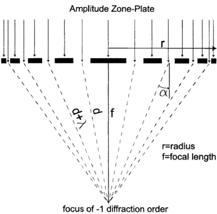
has been in x-ray confocal microscopy. Not until [9] have zone-plates been applied to the context of lithography. To understand the research presented in this paper, it is sufficient to think of the zone-plate as a positive refractive lens.
Thorough theory and simulation of the zone-plate is presented in [16]. The fab-rication procedure of zone-plates can be found in [13]. In this section, an intuitive description of the plate behavior is discussed. Taking a cross-section of a zone-plate (as in Figure 1-2) we observe a grating with decreasing period as we move away from the center of the structure. Each period of the grating is defined as one zone. As the zone period (p) become smaller, the light diffracts at a larger angle (OZ) as is given by Equation 1.2.
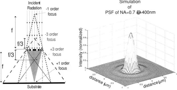
The zones are sized such that the first diffracted order from all the zones crosses the optical axis at the same spot, called the focal point. The writing capability is characterized by the intensity distribution at the focal plane, called the point-spread function (PSF). Moving toward finer features requires engineering a narrower PSF. Figure 1-3 shows a simulated PSF[16].
Amplitude Zone-Plate
1111
\ \ a ~ a \ \ \ \ \ x \ \\ \\~Q
\\\\~~7) ~
\ \ a \\ \ \ \\ ~ a \\ \ ar
-
I-
/-
~,.
I / I / / aicxl,'
,/ a / / /f
a ,/ / / / / /r=radius
f=focal length
focus of -1 diffraction order
Figure 1-2: Cross-sectional view of an amplitude zone-plate. The optical path of the radiation is traced to the first-order focus. It is important to note that the fo-cussing effect comes from diffraction rather than refrac-tion
A
sina (1.2)
Figure 1-3 is a more comprehensive representation of the other diffracted orders created by a zone-plate. The +1 order is used for lithography, and the light associated with the other diffracted orders contributes to background.
Incidert Radation
f/3
f/3
1f
j,
,;
-1 order focus -3 order focus +3 order focus +1 order focus - 08 E08 0.6, C) Substrde Simulation PSF of NA=0.7 @:400nm0.5
0 0.Figure 1-3: (Left)Figure depicting the focal points
asso-ciated with the +1, -1,+3, -3 diffracted orders. The +1 is used for lithography. (Right)Simulated
point-spread function for a NA=0.85 zone-plate operating with a source of A = 400nm.
Extendibility with Source Wavelength
A very important implication of using diffractive optical elements is that they can be created for a photon of any operating wavelength [11]. This addresses a significant hurdle that must be overcome by the semiconductor industry, which has relied on refractive optics in its OPL lithography tools. The use of refractive optics cannot continue as sources below A = 157nm are adopted.
1.2.2
Micromechanics
The micromechanical elements are responsible for modulating the incident beam to each zone-plate independently so that each zone-plate can write a unique pattern. The evolution of MEMS (Micro Electro Mechanical Systems) technology has naturally led to the creation of microscopic spatial light modulators (SLM). These micromechanical systems have a panoply of applications including optical routing, video projection and lithography.
The device selected for the ZPAL application is the Grating Light Valve (GLV(TM)) made by Silicon Light Machines(TM)[7]. The GLV is a one-dimensional array of 1088 spatial light modulators. Figure 1-4 depicts one of these micro-SLMs. There are three prominent reasons why this technology was selected for ZPAL [12]:
1. The GLV provides 8-bits (256 levels) for intensity gray scaling.
2. The GLV has a frame-rate4 of over 350 kHz [22].
3. Diffractive operation as opposed to reflective operation.
Gray-scale intensity modulation is a key function of the SLM in the context of lithography. In practice it is necessary to expose pixels on the wafer with gray level intensities in order to finely control linewidth. This pixel-dependent dose modulation is known as proximity-effect correction (PEC). Many of the commercially available micromechanics simply offer binary modulation schemes (e.g. Texas Instruments DMD(TM)). Binary intensity modulation requires that the dose on the wafer be modulated through time multiplexing. This scheme is more complicated and slower than the real-time intensity dose modulation the GLV provides[10].
Because, the GLV operates on the principle of diffraction rather than reflection, it is able to achieve greater image contrast. The principle behind the optical operation of the GLV will be discussed further in Section 3.2.
4
Moving Ribbon
Fixed Ribbon
Silicon Substrate
Three cells
Incident Radiation
1
rcer
iff r-d-tio 1
Zone-Plate
-
Array
Figure 1-4: (Top) Drawing of a single GLV pixel.
(Bot-tom) Simple one-to-one mapping of GLV pixels to zone-plates.
1.2.3
The ZPAL Test-bed
Upon publishing the original proposal, the NanoStructures Laboratory moved forward with proving the lithographic performance of zone-plates by designing a zone-plate test-bed (Figure 1-5). The first experiments were conducted with A = 193nm [9]. Because of complications with the former sources, a A = 400nm source was adopted for the ZPAL test-bed. Specifically, a 25mW GaN diode laser manufactured by Power
Technology,Inc [1].
Phase zone-plates were designed and fabricated [13] for operation with A = 400nm. Phase zone-plates offer four times the efficiency of the amplitude zone-plates described in Section 1.2.1. By making the opaque regions transparent and introducing a 7r
phase-shift (A/2 delay) relative to the transparent zones, the focussing efficiency into the
+1
order is quadrupled. The numerical apertures for these phase zone-plates ranged from NA=0.7 to NA=0.95. In addition, an array of one-thousand zone-platesPattern inAnalog
main memor Output Boad
IBM PC, Windows 2000, LabView analog drive line
modulated beam Laser (400nm) Conoptics SLM 0611"~ Zone-plate array (focussing elements) Wafer Stage Wafer
Figure 1-5: The zone-plate test-bed architecture. This scheme does not address the multiplexing nature of the ZPAL concept. A single SLM is used rather than an array of micromechanical SLMs. By making the beam broad, the light from a single SLM can illuminate an entire array of zone-plates.
shows the array and a closeup of the zone-plates[llj.
1000 Zone Plates for X = 400 nm, with NA = 0.7 and Focal Length = 40 pm
Areal Coverage ~ 9 mm2
78.4 ptm 39.2 pm
SiO2 HSQ
Figure 1-6: A zone-plate array was fabricated to demon-strate the effectiveness of having many zone-plates writ-ing in parallel. The array shown contains 1000 zone-plates and was written with e-beam lithography using HSQ negative resist
Between the laser source and zone-plates an acoustoptic SLM manufactured by ConOptics[2] was inserted into the optical train. This instrument can achieve suf-ficient contrast(Equation 1.3) and modulate the beam intensity at high speeds (on the order of 10 MHz). This global SLM addresses all zone-plates in the array with the same modulation which means that every zone-plate in the array writes the same pattern. The goal in designing the test-bed was to test the lithographic performance of zone-plates in an array, not the multiplexing nature of the ZPAL architecture.
Imax - Imin
Imax - Imin
The optical elements were then combined with a scannig stage. The stage se-lected was the piezo-controlled Physik Instrumente P-770[3]. The stage is equipped with capacitive sensors which allow closed loop control. The scanning range is 200[m in both the x and y direction with an accuracy of ~ 10 nm[13]. The control hardware and software were configured to raster-scan the stage.
Results
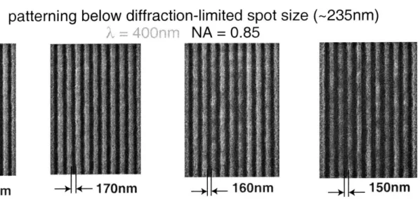
The test-bed system yielded several important results on the lithographic perfor-mance of zone-plates. Some of the key results are shown here. To all users, especially those in the semiconductor industry, resolution is a critical metric. The factor k, in Equation 1.1 is a figure of merit for the resolution capabilities of the overall lithog-raphy system. In the semiconductor industry, the OPL tools operate in a region of
k, =0.40. ZPAL can achieve a k, factor below 0.35 as is shown in Figure 1-7 [16].
patterning below diffraction-limited spot size (-235nm)
A
NA=
0.85
180nm
170nm
160nm
150
Figure 1-7: Patterning result of dense lines and spaces by the ZPAL test-bed demonstrating ki of 0.32 which is on the frontier of lithographic performance
The test-bed proved that an array of zone-plates could arbitrary geometries and write in parallel with sufficient contrast. Because only 40% of the total incident radiation is focussed by the zone-plate, the rest of the light contributes to background.
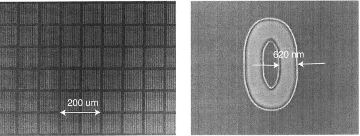
If sufficient contrast does not exist, then the hackground radiation becomes significant and the patterns in the photoresist would wash out. Figure 1-8 shows magnetic ring structures patterned by ZPAL
[15].
Because, the pattern is periodic, the test-bed is ideal for printing them. The rings were written over an entire zone-plate field which is 100 x 100pm2Figure 1-8: (Left) Large array of magnetic memory ele-ments printed using ZPAL test-bed. (Right) A zoomed view of a single memory element.
1.2.4
Evolution from ZPAL Test-bed to ZPAL Prototype
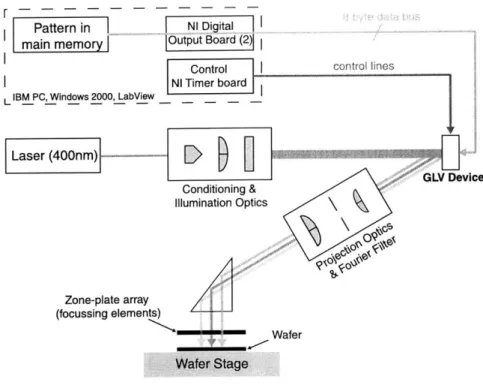
The integration of the GLV micromechanics with the ZPA L test-bed is a key milestone in demonstrating the efficacy of ZPAL as a true parallel patterning nanolithography tool. Compare the prototype system architecture shown in Figure 1-9 with the test-bed architecture depicted in Figure 1-5 description. The key modification is the substitution of the Conoptics single SLM with the array of SLM's provided by the GLV.
Integration of the GLV will require the development and integration of appropriate electronics and optics. The creation of a high bandwidth data-delivery architecture to send pattern information to the GLV as fast as possible is a significant challenge. Once the data is successfully sent and displayed by the GLV, an optical channel must
r - - - - ~ ~ - - - -
-Pattern in NI Digita main memor Output Board (2)
L IBM PC,
Laser (
Control control lines Mindows 2000, LabView NI Timer board
400nm) fewrmrnnli GLV Device Conditioning & Illumination Optics\ Zone-plate array (focussing elements) Wafer
Figure 1-9: Schematic of the ZPAL prototype architec-ture including all four primary elements.
be designed to relay the illumination from the GLV to the zone-plates with integrity. Successful integration will result in the only maskless parallel patterning, high reso-lution, high throughput nanolithography tool to date. The design and capabilities of the prototype system will be judged against the patterning results produced by the preceding zone-plate test-bed system.
Chapter 2
The Data-Delivery System
2.1
Scale of the Data-Delivery Problem
ZPAL is unique to the maskless lithography tool market primarily because of its promise to offer a high throughput massively parallel architecture. This, in turn, pressents the formidable challenge of designing a data-delivery system that satisfies the throughput requirements.
While the aim of the research presented here is not to deliver on the end goal of one wafer per hour (WPH), it is relevant to briefly discuss the magnitude of the data-delivery problem. As of 2003, the semiconductor industry has begun fabricating 300 mm wafers with 100 nm features. A 100 nm square feature is defined by four pixels, each 50 nm square1. To pattern one WPH, the pixel-rate soars to over 7.85Gpix/s as is calculated in Equation 2.1.
300 x 10' nm 2 1 1
0 x 1= 7.85 x 1 0 9lPlx (2.1)
2 2 3600s 550nm s
pix
Making the reasonable assumption that one pixel contains one byte of information, the data-rate is 7.85 GB/s. This throughput is very difficult, given real-world band-width constraints. Intrachip bandband-width in modern day personal computers begins to
'The pixel is smaller than the minimum feature size in order to allow for accurate line-edge placement
approach the required value. For example, the bandwidth between main memory and the processor in an Intel(TM) Pentium(TM) 4 computer with the Intel 875P chipset is
6.6 GB/s [4]. If a similar channel between the data and the modulating device can be
created, then the system is physically realizable. However, there are other bottlenecks in the data-path such as the hard-disk. In maskless lithography, where pattern data can exceed 100 GB, it is inevitable for data to be stored on hard-disk. The bandwidth from a state-of-the-art 15k RPM harddisk to main-memory has a sustained transfer rate between 49 MB/s and 75 MB/s [5]. The key to ZPAL throughput is designing a hardware and software architecture that makes this bottleneck transparent.
The engineering challenge is formidable. Improvements in technology coupled with intelligent data compression algorithms will be required to accommodate the extraordinary data-transfer rates. A research group at the University of California, Berkeley is trying to build an end-of-the-roadmap maskless lithography tool which aims to supplant OPL at the end of the decade. For this tool, the intention is to pattern 60 WPH with 50 nm features. The data-rate for a system with these specifications is an extraordinary 9.4 Tb/s [8]. The ultimate solution proposed to the problem is an architecture where data is compressed as it passes through bottlenecks and is decompressed in real-time when the bandwidth is available [8].
2.2
The ZPAL Data-Delivery Prototype
Require-ments
At the NanoStructures Laboratory, the goal is to build a prototype using the GLV that can write a 0.25 sq.cm (2.5e13 sq. nm) area with 210 nm features in twenty minutes [12]. The pixel size will be 70 nm square. A pattern with that area and pixel size contains roughly 5.10 GB of data. The minimum system bandwidth is 4.25 MB/s. Given the computing power available in current personal computers, achieving such a bandwidth is reasonable without data compression.
2.2.1
GLV Algorithm
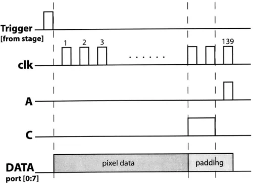
The GLV has a data uploading algorithm implemented in hardware. There are 1088 pixels in the GLV, however packaging limitations prevent each pixel from having its own input line. Therefore the data I/O lines to the GLV are shared. To offer high bandwidth, the GLV offers eight bytes of parallel data input per clock cycle. Therefore data to the GLV is uploaded in a staggered manner over 136 clock cycles. The algorithm below clarifies the uploading algorithm. [20]
// data uploading algorithm for displaying one GLV frame // the frame 'x' is an array of 1088 bytes
i=j=0; x=array(1088);
trigger(A) // begin-dataupload
for(clk=0; clk<136; clk++)
{
i=1+4*clk; j=545+4*clk;
loadpixels(x[i+2] x[i] x[j+2] x[j] x[i+1] x[i+31 x[j+1] x[j+3]);
// in first clock cycle GLV elements 1,2,3,4,545,546,547,548 are
//
updated
}
trigger(C); // display
The GLV will only begin accepting data if it is triggered to do so by a pulse on the 'A' line. The data is locked after 136 clock cycles by triggering the 'C' line. Only after the data is locked is the frame displayed by the GLV.
2.3
Hardware Architecture
There are three key characteristics that will be valued in the design of the hardware infrastructure: flexibility, design time and performance that meets or exceeds the con-straint in 2.2. Balancing the trade-offs between these three arenas creates a genuine
engineering challenge.
Designing an application specific integrated-circuit (ASIC) to control the flow of data through the system will provide the best performance. However, such an approach will lead to significant design times and create a stricture against future changes. An alternative solution is to use off-the-shelf hardware that can be pro-grammed with software. The development time will be cut significantly and perfor-mance should still be able to meet the specification outlined above[23].
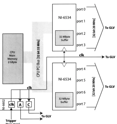
For the prototype, the latter approach was selected. A suite of hardware and soft-ware tools offered by National Instruments (NI) was selected for its balance between performance and configurability. The hardware foundation is an Intel Pentium III processor accompanied by two gigabytes of memory and an 80 GB hard-disk. The computer runs the Microsoft Windows 2000 (TM) operating system2 To this basic
platform three NI boards are connected to the PCI bus of the computer. There are two NI-6534 Digital I/O cards and one NI-6602 timer/counter board [18][17]. These hardware elements can be programmed in the LabVIEW(TM) development environ-ment.
The three NI boards are physically linked via the Real-Time Serial Interface (RTSI) bus which is external to the PCI bus. This direct connection allows for control signals to be distributed with high precision and without the uncertainties of external interrupts.
Figure 2-1 shows how the respective components were configured and interfaced with the GLV. All the lines going to the GLV represent a physical connection between the computer and the GLV board. The control lines and data lines from the NI-boards
2
Ideally, an operating system with minimal overhead (no extraneous processes and small memory footprint) would be used to maximize performance. Microsoft Windows is advantageous because of available tools and drivers for the NI hardware.
NI-6534 CPU Main r Memory 2 GByte
CO
NI-6534 clk C4~32
MBye 0 1 buffer clk A C z To GLV Trigger [from stage] port 0 port 1 4 To GLV port 2 port 3 cik 0 To GLV port 4 port 5 C4 To GLV port 6 port 7Figure 2-1: Schematic demonstrating how the CPU and the NI cards were configured and interfaced to the GLV.
are mapped to the connectors for the GLV through a custom adaptor board. Fig-ure 2-2 is a timing diagram relating the hardware signals to the GLV data uploading algorithm discussed in Section 2.2.1
Trigger
[from stacik
A
C
I
I
g
1 23
H
139
DATA
pixedata port [0:71Figure 2-2: Timing diagram capturing the data upload-ing algorithm.
The NI-6602 is responsible for regulating the flow of data by receiving an external trigger, generating the clock for the NI-6534 output boards, and sending the control signals to the GLV.
The two NI-6534 boards together offer eight bytes of parallel digital output which is the amount of data uploaded to the GLV each clock cycle (reference Section 2.2.1). Each card contains 32 MB of on-board memory for buffering. Buffering allows for the independence from latencies and other bandwidth constraints that exist because of the computer's PCI bus. The maximum clock frequency for the NI-6543 is 20MHz which means that a data throughput of 160 MB/s (over 1 Gbps) can be achieved once data is buffered. Therefore, if the NI cards had infinite memory for buffering, the NI components exceed the performance specification in Section 2.2. However, because memory is limited to only 64 MB, this system must interact with external
components such as the hard-disk and the PCI bus which have their own handwidth
constraints.
2.4
Software Architecture
2.4.1
Validate Functionality of Hardware
After implementing the data-delivery hardware, a first-pass software3 program was developed to demonstrate the functionality and throughput of the data-delivery sys-tem [12].
# of iterations
N N N
Generate Frame Move data from
and store in Memory -- Format all Frames Memory to Opu Frme NI-6534 buffer to GLV
Size of data = N*1088 bytes Bandwidth=160MB/s
RUN
Figure 2-3: A block diagram of the data-delivery archi-tecture created in the first iteration. The entire process is conducted in real-time.
In this first software iteration, all data creation, data processing and data delivery is executed in real-time (see Figure 2-3. In the first phase, a set of data frames is generated and stored in main memory. A frame is the data-structure representing one state or flash of the GLV. A frame is an array of 1088 elements4 where the first element maps to the first GLV pixel, the second element to the second GLV pixel and
so forth.
To make analysis straightforward, a set of frames alternating between all 1088 elements being set to 0 (unactuated state) and 255 (actuated state) is generated5. The mass of data, stored in main memory, is formatted by the processor to comply with the data-delivery system uploading protocol. Upon completion of the processing, the
3
written in LabVIEW 4
Each element stores one byte of data for 255 levels of gray-scaling.
5
To an observer watching the modulation of the light by the GLV, no light would be observed
going into the first order when the first frame is displayed. When the GLV switches to the next frame, light is directed into the first order.
data is transferred in its entiretv from main-memory to the NI-6534 board buffers 6
. Once the transfer is complete the data for a single frame is uploaded to the GLV
(1088 bytes) and then the GLV is triggered to display the frame. The transfer speed
between the NI-6534 cards and the GLV was fixed at 8 MB/s. This sequence of uploading and displaying continues at a constant rate until the buffers have been emptied. Operation of the hardware is observed through the on/off modulation of the first diffraction order. Figure 2-4 shows the experimental setup for observing the modulation of first diffracted order[12].
Helium Neon Laser
( 6 3 2 n m)p ho to -d e te cto r collimating optics focusing lens GLV 1 st order diffracted beam
Figure 2-4: Optical setup for testing functionality and throughput of the data-delivery system. When data for any GLV element is 0, no light goes into the 1st order. However, if the data is 255, then light is modulated into the 1st diffracted order which can be detected by a pho-todiode.
This version of the software demonstrates the ability of the hardware to send data to the GLV. Figure 2-5 shows experimental data recorded on a photo-detector for alternating frames of 0 and 255. Note the peak throughput observed of 1 Gbit/s is commensurate to the maximum capabilities of the NI-6534 boards [123.
However, there are two major shortcomings to the architecture. First, while the peak data transmission shown by Figure 2-5 has sufficient performance, the sustained
real-time data throughput, which is shown in Figure 2-6, is orders of magnitude slower 6
Data-throughput of 1.16 Gbps
Demonstrated
66. kH
Detector
Response
00
10
20
30
40
50
Time (p seconds)
Figure 2-5: This figure charts the modulation of the GLV as observed by a photo-detector. One period on the graph corresponds to sending two data frames to the GLV. One to set all pixels to 255 and a second to set all pixels to 0. The data rate shown is approximately 1 Gbps. Note that this data throughput is the peak data throughput.
and unacceptable for the prototype specifications. Ideally the cycle delay (the time to generate and output data) should be an O(n) process. However, Figure 2-6 shows that the process has a complexity of O(n2) which is unacceptable for a system that
must output more than one million frames. The overall data throughput falls to less than 50 kBps for a data set of ten thousand frames. This means that in real-time operation, the program runs for several minutes. For a maskless lithography tool, the same process needs to happen in the blink of an eye.
Real-Time Performance of 1st Generation Software Architecture
900 0.35 800 - - - -. -. -0.3 --700 -. .. . . . . 0.25 6 0 0 - -- - .-.-.- .- . --. -CDC
~500
---- - - - -0.2 - -- - -- -- -o 0. -200 (101- - 300-0.1 200-0 .200-0 5 - - -- --- - -- -100 0 2000 4000 6000 8000 10000 0 2000 4000 6000 8000 10000 Number of Frames Number of FramesFigure 2-6: (Left) Plots the time required to generate and output increasing number of frames for the first genera-tion software architecture. The complexity of the opera-tion is O(n2
). (Right) Plots the system throughput with
respect to the number of frames. The real-time through-put is significantly below that required for a maskless lithography tool. [12]
Beyond improvement in data throughput, the software and hardware needs to accommodate an external trigger (generated by the stage) to control the frame-rate. The flow of the data cannot be constant. It should be synchronized with an external signal generated by the stage electronics. The stage is responsible for knowing where to place the pixels on the wafer. The stage control electronics, developed as part of the test-bed architecture, Section 1.2.3, can be considered a black box with an output
signal that will trigger the spatial light modulator when the stage reaches the next pixel on the wafer.
2.4.2
Architecture to Improve Real-time Throughput
From experimental results obtained in the first iteration of the software, it was de-termined that the generation and formatting of the data was the major bottleneck. Figure 2-3 charts the flow of the real-time process in the first generation software. Memory allocation has tremendous overhead and should be converted from an 0(n) process to an 0(1) process. In other words, the memory should be allocated only once for all the frames rather than in an iterative approach as each frame is created. Formatting the arrays of the data requires processor involvement, which presents a bottleneck.
# of iterations
N N N
Generate Frame Move data from
and store in Memory Format all Frames Memory to
Outo
ameNI-6534 buffer
Size of data = N*1088 bytes Bandwidth=160MB/s
offline RUN real-time
Store Data to Preload text file ASCII text file on -on hard-disk
Hard-disk into Main Memory
Figure 2-7: A block diagram of the data-delivery archi-tecture created in the second software iteration. The in-novation in this architecture is the idea of breaking up the process into offline and real-time components.
In order to accomplish the data throughput required by a maskless prototype tool a
novel software architecture was developed that splits the data-generation/formatting
and data-delivery process into two stages: off-line and real-time. Figure 2-7 details the data flow within this architecture. The data generation and all formatting is done off-line. This frees the system of a tremendous data processing burden during real-time operation. Prototype software written in the PERL programming language was initially developed to test the concept of offline computation. The formatted data is
written as an ASCII text file saved on disk. Once saved, the data only needs to be loaded to the NI-6534 memory buffers. The processor does not need to interact with the data in any form. The correctness of this design was tested by the experiment in Section 2.4.1, except substituting the real-time data generation and formatting with the offline version. Figure 2-8 charts the significant improvement in bandwidth over the bandwidth presented in Figure 2-6.
Real-Time Performance for 2nd Generation Software Architecture
2 6 1.8 - - - - -5.5 - - - --1 .6 - - - -- --.-.- -.. --.- -5.. 1.4 --4.5 . --.-. T 1.2 - - - -... - -. - --- -. -- - -.--- -- . --D~ 4... o . -- - -0 .5 F- 35 . . . ... ... .. 0.8 0.6 - . . . 0.4-2. 0.2- 2 0 2000 4000 6000 8000 10000 0 2000 4000 6000 8000 10000 Number of Frames Number of Frames
Figure 2-8: (Left) Plots the time required to send increas-ing number of frames for the second generation software architecture. The algorithm demonstrates a linear pro-gression which rather than an exponential one. This is critical as the number of frames going through the system exceeds one million. (Right) Plots the system throughput with respect to the number of frames.
The new architecture demonstrates an 0(n) or linear complexity. This is critical as the number of frames processed by the maskless lithography tool exceeds one million. Intuitively, once the data has been created and formatted, the delivery to the GLV should be a linear operation. Rather than seeing the data throughput fall as the number of frames increases, the new system sees an increase in throughput as the number of frames increases. This is due to the fact that there is overhead
in transferring data. The overhead is nearly constant whether transferring large quantities of data or small quantities of data. Therefore, the overhead is amortized more efficiently when the data set is large, which accounts for the increase in overall throughput. However, the throughput approaches an asymptotic value near 6 MB/s. This sustained real-time throughput exceeds the prototype requirement.
Performance Comparison .3 10 10 version 1.0 0-01... : .- I..: . ... a) .~ .. . 0 1 version 2.0 10-version 1 0 10 2000 4000 6000 8000 10000 100 200 4000 6000 8000 10000
Number of Frames Number of Frames
Figure 2-9: (Left) Compares the cycle delay with the two
different data-delivery architectures explored. (Right)
Plots the real-time system throughput
The dramatic performance improvement between the architecture in Figure 2-3 and Figure 2-7 is most dramatic when compared graphically as it is done using log scale in Figure 2-9. While the functionality is exactly the same, the performance difference is three orders of magnitude.
The ability to break up the data-delivery process into real-time and offline compo-nents is enabled by the availability of large low cost memory on hard-disk. However, by saving the file on disk we introduce a new bottleneck not present in the architecture in the original software architecture. Reading data from disk is orders of magnitude slower than accessing data from main memory. Along with reduced bandwidth, the
transfer from hard-disk adds temporal uncertainty to the data path7. To bypass this bottleneck, the data on disk is preloaded into the CPU main memory just before the system goes online.
2.4.3
Front-end Software
In Section 2.4.2 the frame data sent to the GLV was arbitrary. However, for a maskless lithography tool, the frame data becomes a function of a specific pattern to be printed. This section describes the front-end software algorithm implemented to translate a two-dimensional pattern into a set of GLV frames which can be piped into the data-delivery system described above.
Creation of a Two-Dimensional Pattern
Before one can design a user interface to the prototype tool, whatever the application, the user and his needs must be understood. In this case, the prototype tool will be used by students and other researchers affiliated with MIT. To them, the implemen-tation of the maskless tool should be transparent. They should be able to bring an arbitrary binary pattern stored in a standard file format, whether it be an electronic circuit or an integrated-optical device8, and simply press RUN. The output of the system should ideally be the same binary pattern printed in photoresist.
In the case for the ZPAL prototype, the '.kic' file format was adopted '. This was selected because of its ease in interpretation and its pervasiveness among nanofabri-cation users at MIT.
The '.kic' file generated by the user becomes the input into the ZPAL data-delivery engine. The '.kic' file is converted into a black and white bitmap where each bit represents one pixel in the pattern. The bitmap of the pattern can then be run through a proximity-effect-correction algorithm. By doing so, the black and white bitmap is converted into a gray-scale map. This process requires significant computation and
7
This phenomena is due to the rotation of the hard-disk platter 8
adhering to the resolution limits of the system
is performed offline.
Build and Process Frames
The two dimensional gray-scale bit-map must be converted into a sequence of frames that can be input into the data-delivery engine (Figure 2-7) and will be ultimately displayed by the GLV micromechanics. The pattern must be fractured by dimensions of time and space. First, let us re-examine the writing strategy for the ZPAL proto-type. A global pattern is broken up into square fields1 0. Each zone-plate is assigned to write one field. During a write, the wafer is raster-scanned until the zone-plate has covered its entire field.
Algorithm
Each zone-plate (Z,) is assigned field (F), where N is the total number of fields and zone-plates. Assuming that the fields are square, each given field is composed of M x M pixels (P,,) as is shown in Figure 2-10. Each pixel in the pattern has a unique index which correlates to its frame"1 number i and field number n. The user pattern, which begins as a series of fields, must be translated into frames (R) that can be displayed by the micromechanical system". If the field size is M x M, then the total number of frames will also be M x M.
Zn, F, Pi,,, Ri : 1 < n < N, 1 < i < M
xM
(2.2)
The pixels P,n for any given field, Fn, are sequenced from i = 1 through
i
= MxM as is shown in Figure 2-10. This sequencing is a function of the raster-scanning scheme.Each frame R, is an array of pixel data. The frames are built using the algorithm below:
10The size of the field is equal to distance between adjacent zone plates center to center
"The variable i can be thought of as the chronological sequence of a pixel in a given field 12The algorithm uses frame as a data abstraction so that any micromechanical element can be used
// Pattern to Frame Conversion Algorithm for{i=1; i<=MxM; i++}
{
R-i = [P_{i,1}, P_{i,2}, P_{i,3}... P_{i,N-1}, P_{i,N}];
}
Figure 2-10 describes pictorially how the algorithm maps a given pixel of a given field to a specific frame. It is important to note that the algorithm is 0(1) with respect to the number of zone-plates used and is O(M2) with respect to the size of the field.
The algorithm supports the idea that it is better to write smaller fields with more zone-plates than it is to write larger fields with fewer zone-plates. This assumption depends on the complexity of the frame formatting algorithm done subsequently. For the specific frame formatting algorithm in our system1 3, the complexity for formatting frames is 0(1). Only when the problem has a complexity of 0(n) does it play a significant role in the algorithm efficiency.
User Pattern
Field F
M *-GLV Frames
Frame R.
Frame Rj
~
1 -- +1,1f+1,2
IFrame Ri
-- - -II--+2,1 +2,2 '.ZNote: pattern shown is arbitrary
Figure 2-10: (Left) An arbitrary field is shown along with its pixels and their sequencing. (Right) A set of three arbitrary frames. For a system using the GLV, N < 1088
I . I +1,N
+2
... P+2,N
Chapter 3
Design and Test of the Projection
Optics
3.1
Projection Optics Requirement
The ZPAL prototype requires an optical system to optically map pixels on the mi-cromechanical spatial light modulator to their respective zone-plates. It is best to start by recognizing the zone-plate array as an array of circular apertures with a fixed diameter and pitch1 . What the zone-plates do to photons should be transparent to the preceding optical system. However, it is important to reiterate that zone-plate illumination should contain only one spatial frequency, that of o = 0 (normal
inci-dence) and have uniform intensity. In simulations[16], normally incident light was shown to produce the tightest point spread function. Unlike their refractive coun-terparts, off-axis illumination tends to create aberrations in the focal spot of the zone-plate. When illuminated by multiple spatial frequencies a blurred focal spot will be produced by the zone-plate.
1Pitch refers to the distance between two adjacent zone-plates center to center
3.2
The Optical Operation of the Grating Light
Valve
Until now, the Grating Light Valve has been treated as a black box containing 1088 micromechanical elements capable of modulating light intensity within 256 gray levels. In this section, the optical behavior of the GLV is discussed in order to build a foundation for the projection optics design.
3.2.1
Physical Description of GLV
Each of the 1088 micromechanical elements in the GLV is a reflective phase grating as shown in Figure 3-1. The phase grating structure is created by six reflective Aluminum ribbons. The ribbons are 100 pm long and approximately 4.1 Pm wide making the physical dimension of each GLV pixel 100pm x 25pm. As is shown in
Figure 3-1, there is an alternation between fixed ribbons and deflectable ribbons.
Silicon Light Machines GLV
Deflectable Ribbon
Air Gap
Fixed Ribbon
Silicon Substrate
Single GLV Cell
6 Ribbons
Figure 3-1: A cartoon of a single GLV cell.
The three fixed ribbons are statically held in the same plane. The three deflectable ribbons can be dynamically pulled down together with an electrostatic force. In the unactuated state, all six ribbons are at the same plane, and the element behaves like a mirror by reflecting all light into the zero order. However, if the deflectable ribbons are displaced by some distance, 5, the structure becomes a phase grating. In this actuated state, the light is modulated into several diffraction orders. Figure 3-2