HAL Id: hal-03114421
https://hal.archives-ouvertes.fr/hal-03114421
Submitted on 18 Jan 2021HAL is a multi-disciplinary open access archive for the deposit and dissemination of sci-entific research documents, whether they are pub-lished or not. The documents may come from teaching and research institutions in France or abroad, or from public or private research centers.
L’archive ouverte pluridisciplinaire HAL, est destinée au dépôt et à la diffusion de documents scientifiques de niveau recherche, publiés ou non, émanant des établissements d’enseignement et de recherche français ou étrangers, des laboratoires publics ou privés.
Organic photodetectors based on supramolecular
nanostructures
Yifan Yao, Yusheng Chen, Hanlin Wang, Paolo Samori
To cite this version:
Yifan Yao, Yusheng Chen, Hanlin Wang, Paolo Samori. Organic photodetectors based on supramolec-ular nanostructures. SmartMat, 2020, 1 (1), �10.1002/smm2.1009�. �hal-03114421�
1
Organic photodetectors based on supramolecular nanostructures
Yifan Yao,1 Yusheng Chen,1 Hanlin Wang,1 Paolo Samorì1*1 Dr. Y. F. Yao, Y. S. Chen, Dr. H. L. Wang, Prof. P. Samorì
University of Strasbourg, CNRS, ISIS UMR 7006 8 allée Gaspard Monge, F-67000 Strasbourg, France E-mail: [email protected]
2
Abstract
Self-assembly of semiconducting (macro)molecules enables to develop materials with tailored-made properties which could be used as active components for optoelectronics applications. Supramolecular nanostructures combine the merits of soft matter and crystalline materials: they are flexible yet highly crystalline, and they can be processed with low-cost solution methods.
Photodetectors are devices capable to convert a light input into an electrical signal. To achieve high photoresponse, the photogenerated charge carriers should be transported efficiently through the self-assembled nanostructures to reach the electrodes; this can be guaranteed via optimal π-electron overlapping between adjacent conjugated molecules. Moreover, because of the high surface-to-bulk ratio supramolecular nanostructures are prone to enhance exciton dissociation. These qualities make supramolecular nanostructures perfect platforms for photoelectric conversion. This Review highlights the most enlightening recent strategies developed for the fabrication of high-performance photodetectors based on supramolecular nanostructures. We introduce the key figure-of-merit parameters and working mechanisms of organic photodetectors based on single components and p-n heterojunctions. In particular, we describe new methods to devise unprecedented planar and vertical devices to ultimately realize highly integrated and flexible photodetectors. The incorporation of ordered mesoscopic supramolecular nanostructures into macroscopic optoelectronic devices will offer great promise for the next generation of multifunctional and multiresponsive devices.
3
1. Introduction
Organic semiconductors (OSCs) are promising candidates for the realization of high-performance photodetectors, as they possess tunable energy levels and charge transport characteristics.[1-5] OSCs can absorb light at specific wavelengths across a broadest
spectral range, from ultraviolet (UV) to near-infrared region (NIR), via the subtle modification of the molecular structures and bandgap.[3,6-11] This has empowered the
successful development of high-performance polychromatic photodetectors for numerous technological applications including image sensing, optical communication, and photovoltaics.[12-18] However, the library of accessible organic materials possessing
high charge carrier density and mobility is still rather limited. Moreover, when compared to traditional bulk films, low-dimensional organic semiconducting supramolecular nanostructures (OSSNs) usually possess fewer grain boundaries, reduced density of trap states, and on demand structural motif as a result of the programmed molecular self-assembly.[19] Supramolecular self-assembly, utilizing
“bottom-up” approaches, is controlled by weak intermolecular forces such as van der Waals (vdWs) forces, hydrogen/halogen bonds, or π-π interactions which have the unique feature of combining reversibility, directionality, specificity and cooperativity. In such a thermodynamically governed self-assembly process, semiconducting organic molecules with rigid and large π-conjugated core can self-organize into boundary-free and crystalline zero-dimensional (0D), one-dimensional (1D) and two-dimensional (2D) nanostructures.[20,21] OSSNs with mesoscopic dimension (hundreds of nanometers to
micrometers) can fully exploit the intrinsic characteristics of functional organic nanostructures beyond the limitation of isolated organic molecules. By taking full advantage of these structural and electronic features, during the past decades highly sensitive and low-cost photodetectors based on OSSNs have been developed. Moreover, benefiting from the high crystallinity and flexibility, OSSNs based photodetectors for flexible applications have also been successfully demonstrated.[22]
In this Review Article we introduce the most enlightening recently developed OSSNs based photodetectors by presenting their different operating mechanisms and performance optimization in both planar and vertical device architectures.
4
2. Operation principles and components
2.1 Devices configuration and operating mechanisms
Photodetectors are devices able to transform a light into an electrical signal which include two-terminated photodiodes, photoresistors and three-terminated phototransistors. They rely on the basic physical processes of exciton generation, diffusion and dissociation as well as charge extraction at the interface between the active material and the electrodes. They can be categorized into two device types based on the working mechanism. The former, operating without external gate bias, is a standard two-terminal photoresistor or photodiode. The latter, integrating also an external gate bias, is a three-terminal phototransistor.[3] Both photodiodes,
photoresistors and phototransistors can feature either a planar or a vertical geometry (Scheme 1).
Scheme 1. Top: Schematic illustration of the architecture of planar and vertical
photodetectors. Bottom: sketch of the conversion process of incident light to electric current in (left) monocomponent or (right) bi-component (p-n heterojunction) based devices.
5 Photoresistors are two-terminal devices that utilizes the photoconductive effect. They can provide a high photocurrent gain at the expense of a reduced response speed. Photodiodes are also two-terminal devices, displaying a sandwich-like vertical structure, similar to conventional photovoltaic cells, in which an energetic asymmetry is introduced by either using electrodes (i.e. anode and cathode) with different work functions and/or by exploiting as active material a bi-component system comprising an electron acceptor (n-type) with an electron donor (p-type). The presence of a significant difference in the energy levels of the p- and n-type materials generates a built-in potential, which can effectively promote excitons separation and carrier transport. Phototransistors feature a three-terminal configuration like a standard organic field-effect transistor (OFETs) in which the application of a gate voltage generates a vertical electric field that can facilitate the spatial separation of the photogenerated excitons.[23]
When the photodiode is illuminated, the photovoltaic effect governs the whole process, and it is sub-divided into five fundamental physical processes. First, excitons (electron-hole pairs) are generated in the organic active layer upon photon absorption. Second, the photogenerated electron-hole pair diffuses within the semiconducting material. Third, the electron-hole pair dissociates into free charge carriers. Four, the charges migrate towards their respective electrode. Five, the charges are collected by the electrodes.[3,8,24,25] Conversely, for photoresistors and phototransistors, the
photoconductive effect is the prime origin for the generation of a photocurrent. When a voltage is applied, photoexcited charge carriers induced an increase in the carrier density that ultimately yields in an enhancement of the devices’ conductivity. In photoresistors and phototransistors, the photoconductive gain is generated before the charge recombination takes place. Therefore, to obtain high-performance photodetectors, the chosen organic active layer needs to combine (i) high charge carrier mobility to ensure optimal free carriers transport, (ii) ideal built-in potential for the dissociation of electron-hole pairs, (iii) optimized relative energy levels of the components to guarantee enhanced charge injection and extraction at the electrodes-semiconductor interfaces, (iv) high robustness and stability to enable the device
6 operation according to the standards of the electronic industry. Moreover, with the increasing demand of the flexible and wearable electronics, flexibility of the device is becoming a requirement.
2.2 Basic parameters
To evaluate the performance of organic photodetectors, a series of key performance indicators are currently used. In a nutshell, a maximization of the signal-to-noise performance is a prerequisite for developing highly-sensitive photodetectors.
The external quantum efficiency (EQE) is an important parameter for evaluating the photodetector efficiency, which is defined as the ratio between the number of photo-generated carriers and the number of the incident photon. It can be defined as EQE = !!"#$%·#$
%&'·& , where ILight is the photocurrent, h is the Planck constant, ν is the velocity of light, PIn is the incident light power, q is the elementary charge. To reach a large EQE,
the active layer should have high optical absorption and few carrier trap states.[26]
The photosensitivity (P) represents the ratio of light current to dark current. P can be defined as P = !!"#$%'!()*+
!,-./ where ILight and IDark are the drain current under illumination and in dark, respectively. Photoresponsivity is therefore the signal to noise ratio of photocurrent to dark current.
The photoresponsivity (R) is the ratio of photocurrent to incident-light intensity, which can be defined as R = !!"#$%(·%'!()*+
&' =
)*)·+&
#, , where S is the effective device area and
ν is the speed of light. Hence, responsivity is the effectiveness of a photodetector to
convert a given incident optical signal into an electrical one.
Moreover, to precisely evaluate the signal-to-noise ratio, the specific detectivity (D*)
also needs to be considered. Detectivity (D) is used to describe the ability of weak light detection. Its normalized value is named specific detectivity (D*), which can be defined
as 𝐷∗ = ./01
2)3, where A is the working area of the device and Δf is the modulation
frequency of the measurement. Noise equivalent power (NEP) corresponds to the minimum photosensitive power which can be distinguished from noise; it is expressed
7 as NEP = in/R, where in is the noise current, R is the photoresponsivity. If the shot noise,
i.e. the noise originates from the discrete nature of electric charge, becomes dominant over the total noise from the dark current, D* can then be written as D∗ = 4
.5&6()*+, where JDark is dark current density of the photodetectors. In this regard, in order to
achieve high-sensitivity in photodetectors, it is key to maximize the responsiveness and reduce the dark noise.[26-28]
The Linear Dynamic Range (LDR) is a figure-of-merit for photodetectors to establish the light intensity range in which the photodetectors have a constant responsivity. It can be expressed in dB as LDR = 20 log%0)%
%!12, where PSat (PLow) is the starting (or ending) point of light intensity when the photocurrent responds linearly to the light intensity. A wide LDR facilitates quantitative detection and clear imaging.[27]
Temporal response time (t) is the ability of a photodetector to follow a rapidly modulated light signal, which can be defined as the rise time (tr) from 10% to 90% of the peak value and decay time (td) from 90% to 10% of the peak value, accompanying light illumination and turn-off. Photodiodes typically feature values on the millisecond time scale due to the effective separation of the photogenerated electron-hole pairs by the junction of the organic active layer and short charge transfer distance.[29]
2.3 Self-assembly of organic (macro)molecules forming low-dimensional nanostructures
Conjugated organic (macro)molecules, which are typically composed by a rigid aromatic backbone and soft alkyl side-chains, are prone to undergo spontaneous self-assembly, primarily driven by π-π stacking and van der Waals interactions, forming semiconducting highly crystalline nanostructures such as 1D nanowires, nanorods, nanoribbons nanobelts and 2D crystalline (porous) films.[20,30] During the past decades,
both specific processing methods such as physical vapor deposition (PVT), solution epitaxy, solvent phase-transfer (PT), induced precipitation (SIP) and solvent-vapor diffusion (SVD) as well as post-processing procedures like solvent-solvent-vapor annealing (SVA) have been exploited to drive the self-assembly π-conjugated organic
8 materials towards the formation of high-quality supramolecular nanostructures under mild conditions.[21,31] Self-assembly enables to reduce the amount of structural defects
by increasing the degree of crystallinity of the nanostructures. Importantly, the size, degree of crystallinity and flexibility of the obtained nanostructure as well as its numerous physical properties could be tuned by changing the growth parameters, like concentration, solvent type, growth time, temperature, etc. Alongside traditional crystalline 1D and 2D nanostructures introduced above which are physisorbed on the substrate surface, the formation of self-assembled monolayers via covalent surface functionalization represents another powerful tool to integrate an optoelectronic functionality in working devices. Caranzi et al. demonstrated the possibility to fabricate a molecular junction based photodetector by sandwiching a self-assembled monolayer (SAM) of indoline dyes between transparent PEDOT: PSS and aluminum electrodes.[32]
The carboxylic acid group exposed on indoline dye molecules can chemically linked to the native Al2O3 layer coating the aluminum bottom electrodes. Optoelectronic
characterizations of the devices revealed a photoresponse for all the investigated dyes (D102, D131, D205) with a maximum VOC value of 180 mV with dye D205 and a
maximum JSC of 47 nA/cm2 with dye D102. By lowering the contact resistance, the
dynamic response could be largely reduced to 35 μs upon replacing PEDOT: PSS with semitransparent Au.
3. Photodetectors based on planar architectures
Planar device geometries hold huge potential for technological applications because of their greater compatibility with conventional electronics. However, their construction frequently requires the use of sophisticated, expensive and slow tools for nano- and micro-fabrication. To circumvent this problem, one can exploit unconventional nanofabrication techniques like shadow mask, stamping technique, nanoimprint lithography, colloidal lithography, and direct photolithography by integrating as active components supramolecular organic nanostructures.[21]
9
3.1 Single component
One-dimensional (1D) crystalline nanostructures have been thoroughly utilized as active materials in photodetectors because of their unique optoelectronic properties including large charge carrier mobilities and abundance of interfaces for exciton separation as the high surface-to-bulk ratio minimizes the diffusion length from the bulk to the interface where exciton separation typically occurs.[33-35] Moreover, their high
surface-to-volume ratio make them extremely sensitive to external stimuli such as electromagnetic fields.[36-39] Among the optoelectronic devices, organic
phototransistors have been proven to be extremely effective in combining light detection and signal magnification in a single device due to their high photosensitivity resulting from an internal amplification of photocurrent.[40-44] In phototransistors, 1D
nanostructures exhibited much higher electron mobility and photoresponse when compared to their corresponding spin-coated films because of their greater crystallinity (Figure 1a).[45] Interestingly, it was found that the photoresponse of
perylenebis(dicarboximide) (PDI) derivatives could be largely modulated by changing the device geometry. By reducing the channel length, PDI multifiber-based phototransistors displayed a record average responsivity value of 4.08±1.65×10⁵ A W -1 for 2.5 μm channel length being 2-3 orders of magnitude higher compared to the
corresponding thin-film phototransistors (tf-OPTs), as shown in Figure 1a.
Differently from small-molecule semiconductors, obtaining high crystallinity and long-range molecular packing with conjugated polymers requires the use of an ultraslow self-assembly process from diluted solutions in an ambient saturated by certain solvent-vapors. Liu et al. systematically investigated the optoelectronic performance of highly crystalline donor-acceptor (D-A) conjugated polymer (PTz) nanowires in phototransistors, as exemplified in Figure 1b.[46] A facile liquid-solid self-assembly
method was employed to prepare well-defined PTz nanowires directly onto trichloro(octadecyl)-silane (OTS) treated SiO2 substrates from its dilute solution (0.5
mg mL-1 in chloroform). X-ray diffraction (XRD) and selected area electron diffraction
10 assembled structures even displaying single-crystalline domains, with a size on the tens-to-hundreds nanometer, ultimately forming self-assembled nanowires. Such structural analyses suggested thatpolymer chains are aligned along the main axis of the nanowires forming lamellar structures with an interlayer d-spacing of d1=21.05 Å and
a close π-stacking (d2=3.47 Å) perpendicular to the long axis of the nanowires. The
charge transport properties of the nanowires were characterized by fabricating and testing the OFETs, which displayed hole mobilities of ca. 0.46 cm2 V-1s-1, being 4 orders
higher than those measured in devices based on spin-coated films. Phototransistors integrating nanowires with a width around 150 nm showed that upon increasing the channel length the photoresponsivity at VGS=0 V decreases rapidly reaching a plateau
at L = 4 µm (Figure 1b right). In line with previous reports, it was found that the shorter channel lengths enable to reach higher photoresponsivities because of greater photocurrent and increased probability of photoinduced carriers to be collected by the electrodes before recombination.[45] Photoresponsivity up to 2531 A W-1 and
photosensitivities up to 1.7×10⁴ were measured in phototransistors based on individual
PTz nanowires with a channel length of 3.5 µm. These results have fully demonstrated that the photoelectric properties of 1D (macro)molecular (nano)wires can be largely improved by using highly ordered crystalline nanostructures and ad hoc device geometries.
Figure 1. a) (Top) Chemical structures of the alkyl substituted PDIs. Transfer
characteristics of PDI-1 multifiber-OPT at VD = 80 V with L = 20 μm. (Bottom)
Variation of responsivity R and photosensitivity P for multifiber-OFET. Dependence of R on the channel length (L) for multifiber-OFETs upon illumination with monochromatic light. a) Reproduced with permission.[45] Copyright 2012, American
11 Chemical Society. b) (Top) Chemical structure of PTz. (Middle) Optical microscopy images of PTz nanowires on SiO2/Si substrates produced by a 5-to-6 days lasting
self-assembly process starting from 0.5 mg mL-1 solution; SAED pattern of a single PTz
nanowire; and schematic diagram for the possible molecular packing forming the PTz nanowires. (Bottom) R vs channel length. Variation of photoresponsivity and photosensitivity. b) Reproduced with permission.[46] Copyright 2013, American
Chemical Society.
In order to fabricate planar phototransistor based on highly crystalline organic semiconductors, perylene tetracarboxylic dianhydride (PTCDA) nanoparticles with diameters of ~ 80 nm were deposited onto 30 nm-thick silicon nitride (Si3N4) membrane
through thermal evaporation.[47] SAED provided evidence for the single-crystalline
nature of these PTCDA nanoparticles. Novel nanoparticle-based phototransistors were constructed by growing PTCDA nanoparticles inside bowl-shaped pores on Si3N4 and
depositing volcano-shaped Al gate electrodes with Al2O3 insulating layers. The devices
containing only single grains displayed electron mobilities which are 2-3 orders of magnitude higher when compared to conventional film-structured polycrystalline organic semiconductor transistors. Moreover, the devices showed stable switching behavior with the increasing UV light intensity, and the EQE reached a high value of 3.5◊106.
Figure 2. a) (Top) Crystallization process of C60 in bisurea-based derivative/m-xylene
gel induced by acetonitrile. (Middle) Photographs and SEM images of the C60 fibers.
(Bottom) I-V measurements and time sweep of the C60 device with incident light having
different wavelengths. Comparison of time-dependent photoresponse measurement between the original sample and the sample subjected to 200 bending cycles. a) Reproduced with permission.[48] Copyright 2019, Wiley-VCH. b) (Top) Molecular
12 Structures of PTCDI Building Blocks. (Bottom) Photocurrent response of MP-PTCDI nanofibers under ambient conditions with various white light illumination power densities. Photocurrent decay time constant (τ) as a function of illumination power density. b) Reproduced with permission.[49] Copyright 2016, American Chemical
Society.
Fullerene (C60), being one among the most important n-type organic semiconductors,
has been widely used as active material in photovoltaic cells, FETs, sensors, and photodetectors.[50] However, owing to its 0D structure, it is still a great challenge to
drive its self-assembly towards the generation of ordered supramolecular nanostructures.[51] Several sophisticated protocols have been developed to grow 1D C60
crystals including template methods, slow evaporation, liquid/liquid interface precipitation, volatile diffusion, and gel-assisted method. Recently Liu et al. reported an efficient approach to grow high-quality C60 crystal with the help of supramolecular
gels derived from low-molecular-mass gelators (LMMGs).[48] The existence of
supramolecular gel can suppress the sedimentation or aggregation of the crystals. Furthermore, the gel-based 3D networks can provide confined spaces for the organic crystals to grow with either strong or weak coupling between gel fibers and crystals. By making use of this method, C60 crystalline fibers with tunable lengths and diameters
could be easily prepared with a m-xylene gel of a specially designed LMMG triggered by acetonitrile at room temperature. Figure 2a top and middle portray the crystallization process, and the representative optical and scanning electron microscopy (SEM) images of a bundle of C60 fibers growing through the whole gel phase triggered
by an antisolvent, i.e. acetonitrile. The fibers could reach an astonishing length of 70 mm, and the length/width ratio can reach 23 000. Moreover, the lengths of the fibers could be largely tuned by changing the height of the supramolecular gel phase. Top gate FETs based on C60 fibers showed electron mobilities of 1.03 cm2 V-1 s-1. Here, planar
two-terminal photoresistor with crystalline C60 fiber as the active material was used as
the photodetector, Figure 2a bottom displays the voltage-dependent current (I-V) curves of the C60 device recorded in the dark condition and upon irradiation of 300, 400,
13 respectively. The time-dependent current curves acquired while irradiating at these wavelengths and applying voltage of 10 V revealed that the device could respond quickly to the incident light and fully return to the ground state when the light was turned off. More interestingly, the photocurrent and response speed remained unchanged after bending the device supported on the flexible mica substrate under 90° for 200 cycles. These findings suggest that 1D fullerene crystalline fibers hold great potential for application in flexible optoelectronics based on n-type semiconductor. Persistent photoconductivity (PPC) is the photocurrent which can be measured for hours or days after illumination is terminated.[52] It is important to point out that PPC
behavior could severely affect the response speed of the photodetectors thereby jeopardizing the use of organic photodetectors in high speed optical switches. Yet, the PPC behavior opens new opportunities for optical memories, like organic optical imaging circuits, memory devices, and artificial intelligence. Noteworthy, the PPC phenomena from a purely fundamental physics viewpoint is still not completely unraveled.
PPC can be caused by charges trapped at the organic semiconductor/dielectric interface. Defects, which mainly originate from polar functional groups (-OH, -NH2, and -COOH
etc.) on polymer dielectric surfaces, or inorganic dielectric, act as trapping centers for the photogenerated carriers, thus inducing band bending and carrier accumulation in the device channel.[53,54] Recently Jia et al. proposed a new mechanism related to
electrons trapping in oxygen-induced deep levels in organic semiconductors for explaining the PPC behavior in organic phototransistors.[55] To eliminate the possible
influence of semiconductor/dielectric interface and grain boundaries, single-crystalline 2,8-difluoro-5,11-bis(triethylsilylethynyl) anthradithiophene (diF-TESADT) based phototransistors have been fabricated by using divinyltetramethylsiloxane-bis(benzocyclobutene) derivative (BCB) as trap-free polymer dielectric. Nevertheless, PPC was still observed. Further, optoelectronic characterization under air atmosphere and high vacuum, scanning kelvin probe force microscopy (SKPM) and first-principle calculation demonstrated that oxygen molecules in the air play a crucial role in determining the PPC behavior in phototransistors. Oxygen atoms can produce deep
14 levels in the energy bandgap of organic semiconductors, which could trap the photogenerated electrons which could be released long after the light is switched off. As a result, the gating effect arising from trapped electrons can cause a pronounced PPC behavior in organic phototransistors.
In addition to external influences, structural defects within the OSSNs can hinder the recombination of charge carriers thereby yielding cause a significant PPC effect. To gain insight into this issue, a comprehensive study on self-assembled perylene tetracarboxylic diimide (PTCDI) nanofiber has been performed aiming at acquiring a better understanding on the PPC effect.[49] The PTCDI nanofibers were fabricated upon
self-assembly of PTCDI derivatives exposing strong electron donor groups (Figure 2b top). PPC results obtained with the 1-methylpiperidine-substituted perylene tetracarboxylic diimide (MP-PTCDI) nanofibers deposited on the interdigitated electrodes are displayed in Figure 2b bottom. They exhibited high photoconductivity upon illumination, producing a photocurrent on/off ratio ranging from ca. 18 to 71 with the illumination power density increasing from 0.31 to 5.77 mWcm-2 under a bias
voltage of 7 V. After turning off the light, the photocurrent relaxed quite slowly to the dark current level, with a decay rate significantly dependent on the illumination power density (Figure 2b bottom). A comparative study comprising a series of PTCDI molecules exposing different side groups revealed the existence of PPC only in nanofibers grown from the PTCDIs substituted with strong electron-donating groups, such as MP-PTCDI, MT-PTCDI, and MA-PTCDI (Figure 2b top), with a decay characterized by a long tail exceeding 1 h to reach the dark current baseline. In contrast, no significant PPC effect was observed for the nanofibers of PTCDIs functionalized with weak electron donors (e.g., MO-PTCDI, DD-PTCDI, and CH-PTCDI), for which the photocurrent returned relatively quickly to the dark current level in less than 10 s. XRD, Kelvin probe force microscopy measurement and temperature-dependent electrical characterizations provided evidence that the significant PPC effect recorded for MP-PTCDI nanostructures is likely due to the defects formed from the charge separation within the molecular stacks, wherein the electrical potential barrier created around the defects prevents the recombination of the photogenerated charge carriers.
15 The extended electron delocalization along with the π-π stacking (the long axis of nanofiber) further enhances the charge separation, introducing more internal defects, resulting in a more pronounced PPC. These results will help in increase our understanding on the mechanism and design new material structures for sustained charge separation in order to further enhance the photovoltaic and photocatalytic efficiency of organic semiconductor materials.
Compared with one-dimensional nanostructures, two-dimensional structures exhibit unique advantages in terms of physical, chemical, and mechanical properties, as evidenced in the superlative characteristics displayed by their prototypical scaffold, i.e. graphene.[56-60] Their increased dimensionality offers improved percolation pathways
for charge transport around defects, thus allowing to achieve high light responsivity.[61]
Additionally, by taking advantage of their ultrathin structures, the active channel can be fully depleted, resulting in a suppression of the dark current thereby boosting the sensitivity.[26] Fu et al. proposed a novel "phase separation" molecular design strategy
to prepare millimeter-sized monolayer or few-layered 2D molecular crystals (2DMCs) by using solution self-assembly.[62] The designed molecule comprises a rigid
π-conjugated core decorated by soft alkyl chains exposed above and below the molecular core.As a result of the nanoscale phase segregation between the rigid core and the soft alkyl chains it was possible to assemble, via layer-by-layer growth, a few layer thick 2DMCs with lateral sizes on the millimeters scale. Phototransistors based on the 2DMCs showed photosensitivity as high as 2.58×10⁷, a high responsivity of 1.91×10⁴
A W-1, and detectivity of 4.93×10¹⁵ Jones. Impressively, the detectivity of the
2DMC-based phototransistors outperforms most of the organic photodetectors, demonstrating that 2D molecular crystals have huge potential for fabricating high-performance organic photodetectors.
One of the true advances of organic materials is the possibility of tailoring their electronic, optical, and magnetic properties through chemical design, thereby providing an unlimited possibility for various applications. One representative example of such tunability relied on the use of narrow-bandgap furan-thiophene quinoidal compound
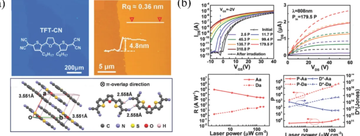
16 (TFT-CN) with strong absorbance at around 830 nm for the fabrication of near-infrared (NIR) organic phototransistors.[63] The millimeter-sized, air-stable n-type TFT-CN
2DMCs with a thickness of 4.8 nm have been grown by "solution epitaxy" (Figure 3a top).[64] TFT-CN 2DMCs was found to adopt a slipped face-to-face packing structure
with a strong π-π partial overlap amounting to 3.551 Å between adjacent molecules in the ab plane of the crystal film. In particular, in the direction almost perpendicular to the π-π stacking direction, strong CN⋯H non-covalent interactions with a distance of 2.558 Å have been obtained thereby yielding a true 2D network (Figure 3a bottom). Due to the single-crystal nature, 2D crystals exhibited efficient carrier injection and intrinsic defect-free carrier transport, thereby leading to excellent responsivity of 9×10⁴
A W-1. Furthermore, in ultrathin structures, the channel could be fully depleted and
operated at an extremely low Ioff in the dark, yielding an extremely low dark current of
0.3 pA and very high detectivity D* value of 6×10¹⁴ Jones under an 808 nm laser
(Figure 3b).
Figure 3. a) Optical microscopy and AFM image of micrometer-sized TFT-CN 2D
single crystal films. Bottom the π-π interactions in the π-stacking, and the CN⋯H (thiophene) interactions perpendicular to the π-π overlap direction. b) (Top) transfer curves of TFT-CN 2D single crystal phototransistor under dark condition or different laser intensities (1P = 1 μW cm-2). Output characteristics of the transistors with different
VGS (black = 0 V, purple = 10 V, olive = 20 V, orange = 30 V, and red = 40 V) under
dark (solid) and laser illumination (dashed). (Bottom) photoresponsivity, the photocurrent on/off ratio and specific detectivity versus different laser intensities in the accumulated area (Aa, VGS = 40 V, solid line) and depleted area (Da, VGS = -2 V, dashed
17
3.2 p-n heterojunctions
The multicomponent self-assembly of p-type and n-type semiconductors, thus containing two or more functional compounds, interacting in structurally defined heterojunction interfaces represents a viable approach to the emergence of novel properties and even multi-functionality.[65-67] Nevertheless, controlled self-assembly
should be exploited to avoid the thermodynamically favored macroscopic phase segregation between the two components and driving the organization towards nanoscaled p-n crystalline heterojunctions which can offer improved exciton diffusion lengths and fast charge transport characteristics, being key for efficient excitons dissociation and photocurrent generation. Hence, p-n heterojunctions are highly relevant in modern electronics and optoelectronics. In 2010, Zhang et al. synthesized
single-crystalline bilayer p-n heterojunctions based on n-type
hexadecafluorophthalocyanine (F16CuPc) and p-type copper phthalocyanine (CuPc)
through the physical vapor transport method.[68] Because of the good crystal lattice
matching between the (001) faces of CuPc and F16CuPc, high quality p-n interface
junctions with a molecular precision could be obtained. The CuPc-F16CuPc nanoribbon device yielded a short circuit current density (JSC) of ∼0.054 mA cm-2, an open-circuit
voltage (VOC) of ∼0.35 V, and an efficiency (η) of ∼0.007% under 1 sun (100 mW cm -2). The p-n nanoribbons represented an ideal platform for unravelling the charge
transport and photovoltaic behaviors in nanoscale organic-organic interfaces.
On the other hand, although p-n heterojunctions of electron donors and acceptors promote the generation of photocurrent, the formation of charge-transfer complex and the lack of long-range charge transport pathway could result in loss of the photogenerated charge carriers through recombination. Che et al. reported a simple approach by using interfacial engineering of electron donor onto acceptor nanofibers via optimization of hydrophobic interaction between long alkyl side-chains to achieve high photoconductivity and fast photoresponse (Figure 4a).[69] Donor molecules are
non-covalently tethered to acceptor nanofibers through hydrophobic interactions involving long alkyl side-chains, yielding an interface characterized by alkyl interdigitation that exhibited tunable photoinduced electron transfer and the charge
18 recombination. High photoconductivity was observed for the nanofibril heterojunctions with a photocurrent on/off ratio exceeding 104 when measured on a microelectrode pair
(90 μm wide and 5 μm gap) under a bias of 10 V. Under 550 nm light irradiation, the quantum efficiency of the photocurrent generation can be estimated as ca. 8% under an electrical field of 2 V/μm. The photocurrent was found also to switch promptly when turning the light on and off (Figure 4a right) with a response time as little as ca. 200 ms. This simple approach to the fabrication of highly photoconductive p-n junction nanofibers can lead to more options for the new materials design and photoresponse performance improvement.
Figure 4. a) (Left) The π-stacking along the long axis of nanofiber is conducive to
enhancement of charge transport. (Middle) Molecular structures of the three electron acceptors (A-1, A-2, A-3) and three electron donors (D-1, D-2, D-3). (Right) Photocurrent measured at 10 V of bias in response to turning on and off the white light irradiation (0.17 mW mm-2). Reproduced with permission.[69] Copyright 2011,
American Chemical Society. b) (Left) 3D schematic diagram of a crystalline heterojunction photovoltaic device based on PTDI-C8 and Dph-BTBT crystals. (Middle) J-V curves of the heterojunction devices in the dark and upon illumination at different wavelengths. The inset shows the open-circuit voltage significantly shifts from 0.56 to 1.4 V when the illumination wavelength changes from 320 to 690 nm. (Right) Photoresponsivity spectra in PC mode (-3.0 V bias) and PV mode (0 V bias), inset shows the HOMO-LUMO energy levels of both materials. b) Reproduced with permission.[70] Copyright 2018, American Chemical Society.
19 Recently, we have microfabricated planar crystalline organic heterojunction devices by using the direct photolithography technique.[70] The organic crystalline donor-acceptor
heterojunction photovoltaic devices was based on planar asymmetric Au-Ag electrodes, n-type nanowires N,N′-dioctyl-3,4,9,10-perylenedicarboximide (PTCDI-C8) and p-type nanoflakes 2,7-diphenyl[1]benzothieno[3,2-b][1]-benzothiophene (Dph-BTBT) as shown in Figure 4b left. By making use of this crystalline heterojunction prototypical device, we have explicitly illustrated energy level effects on short-circuit current and open-circuit voltage and realized large open-circuit voltage modulation from 0.56 V to 1.4 V when the irradiation wavelength is tuned from 320 to 690 nm, which is derived from energy level mismatch (Figure 4b middle). We also have investigated the photoresponsivity of the crystalline heterojunction devices in photovoltaic (PV) and photoconduction (PC) modes at different wavelengths. The photocurrent is apparently determined by the absorption in PTCDI-C8 nanowire and Dph-BTBT nanoflake, as shown in the blue curve of Figure 4b right. By applying a working voltage, the photoresponsivity could be largely enhanced due to the increased width of the depletion junction. For example, the responsivity was found to increase from 0.1 to 1.1 μA W-1 by applying a -3.0 V bias voltage.
4 Photodetectors based on a vertical architecture
Compared to the conventional planar configuration, photodetectors with vertical geometry can be fabricated layer-by-layer more easily, frequently without the use of sophisticated nano- or micro-fabrication set-ups, thus enabling simpler large-scale production. Also, the deposition methods that can be employed to grow the active films can be rather standard including spin-coating, spray-coating, in addition to roll-to-roll and inkjet-printing. From the device physics viewpoint, the shorter channel in vertically stacked electrode can largely reduce the working voltage, shorten the charge transport distance and enhance the exciton separation efficiency. In this section, we will highlight the most remarkable results on OSSNs based photodetectors with advanced vertical configuration.
20
4.1 Vertical phototransistors
Organic vertical transistors consist of a vertical arrangement of a gate electrode, a dielectric layer, a source electrode, an organic channel layer and a drain electrode. The use of porous source electrode or graphene is a viable solution for this kind of architecture, in order to prevent electric field shielding.[71] Recently, by utilizing
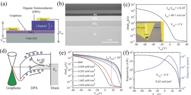
graphene as the source electrode and p-type 2,6-diphenyl anthracene (DPA) single crystal as the active layer, Liu et al. have fabricated vertical phototransistor with the device architecture portrayed in Figure 5a and b.[72] This device exhibited high on/off
ratio of 106 and a high current density of 100 mA cm-2 under voltage of -5 V (Figure
5c). When the DPA single crystal was stacked onto graphene without illumination, the
holes in the DPA single crystal moved to the interface with graphene, and as a result the energy levels of the DPA single crystal near the graphene bent downward. Upon light illumination, the hole concentration of the DPA single crystal increased and the Fermi energy of graphene decreased consequently. Therefore, the barrier height between graphene and DPA single crystals reduced and the drain-to-source current augmented significantly, as shown in Figure 5d. Transfer curves of DPA-based single-crystal vertical phototransistors in the dark and under light illumination with different light illumination intensities are presented in Figure 5e. Under the light intensity of 2.03 mW cm-2, a high photocurrent and high I
Light/IDark=104 were obtained at a positive gate
voltage region. Maximal detectivity (D*) can reach up to 1013 Jones under illumination
intensity of 0.62 mW cm-2, and at V
GS=10 V (Figure 5f). These indicators provide
evidence for the high-quality and high-performance of organic single crystal vertical phototransistors. These results may pave the way towards the developments of other sophisticated vertical organic electronic and optoelectronic circuits.
21
Figure 5. a) A schematic of the cross-sectional view of the vertical phototransistors. b)
Cross-sectional TEM image of a DPA-based vertical transistor. c) Typical transfer characteristics of a representative DPA-based vertical transistor. d) Band diagram of the phototransistors under illumination. e) Transfer characteristics of phototransistors under various illumination intensities compared to that in darkness. f) Photoresponsivity and detectivity as a function of gate voltage. Reproduced with permission.[72] Copyright 2018, Wiley-VCH.
4.2 Vertical photodiodes
Wu et al. have reported p-type, n-type and p-n junction vertical photodiode based on dioctylbenzothienobenzothiophene (C8-BTBT) and perylene-3,4,9,10-tetracarboxylic dianhydride (PTCDA).[73] By exploiting the strong and tunable van der Waals forces,
self-limited organic molecular beam epitaxy method enabled to deposit ordered assemblies of ultrathin organic semiconductors on graphene. Photodetectors were fabricated with the structure of graphene/PTCDA/C8-BTBT/Au. Upon illumination of the PTCDA/C8-BTBT with 514 nm laser, the photodetector displayed high photovoltaic response with open-circuit voltage of ∼0.5 V and photoresponsivity of ∼0.37 mA W-1. In order to fabricate vertical photodetector based on highly crystalline
organic semiconductors, copper phthalocyanines (CuPcs) were self-assembled in the form of nanowires and nano-pillars onto an n-type Si substrate, and then coated with Au thin film. Upon absorption of photon energy the electrons were excited overcoming
22 the Schottky barrier formed on the Au/n-type Si interface, thereby generating a photo current.[74] However, the CuPc nano-pillars assemblies were not dense enough to fully
cover the whole Si substrate; because of this reason gold could have got in direct contact with the Si substrate, resulting eventually in local short-circuits and overall yielding large noise signal in photodetectors. To overcome this problem, a radically different strategy for fabricating novel vertical photodiodes based on nanomesh scaffold, rather than a sandwich structure, have been devised by our group (Figure 6a).[35] Highly
periodic nanostructures could be obtained by making use of nanosphere lithography based on self-assembled colloidal spheres. The produced honeycomb-shaped nanoholes could be filled with different kinds of semiconducting material obtained from small molecules or polymers to meet different application requirements. Upon modification of the Si electrode with a 5 nm thick film of the p-type P3HT followed by a deposition with flexible n-type PTCDI-C8 supramolecular nanowires, the device exhibited outstanding photovoltaic effects. In particular, it displayed high signal-to-noise ratio of 107, excellent external quantum efficiency of >55% and surprisingly ultra-fast
photoresponse time ~10 ns, under photoconduction mode (V = 1.5 V). A further improvement was attained by fabricating bi-crystals heterojunction photodetector based on this vertical-yet-open asymmetric architecture.[75] Figure 6b shows the schematic
diagram of the bi-crystals heterojunction photodetector. TIPS-PEN (p-type) and PTCDI-C8 (n-type) were chosen as active materials due to their high tendency to crystallize in orthogonal solvent and their complementary absorption in the UV-Vis range. The devices displayed ultrahigh signal-to-noise ratio of 107, ultrafast
photoresponse less than 100 ns under four color light irradiation and high sensitivity even though at low irradiation power. Importantly, it was demonstrated that the self-suspended nanomesh scaffold is not only compatible with rigid glass but also with flexible plastic substrates such as PET, as illustrated in Figure 6c.[76] After 1000
bending fatigue test, the photoresponsivity of PET supported photodetector decreased slightly to 79%, thus revealing an overall good robustness enabling the nanostructure of the hollow nanomesh scaffold to retain ultralow leakage current. Notably, the flexible bi-crystal PV detector revealed a faster photoresponse time being as low as 8 ns.
23
Figure 6. a) Cartoon illustration of the high-density nanowire devices realized by the
vertical-channel nanomesh scaffold. Optical microscopy and AFM/SEM images of the high-density nanowire photodiodes. Calibrated EQE for both the large-area and small-area PTCDI-C8 supramolecular nanowire devices. Transient photocurrent as a function of time for P3HT/PTCDI-C8 nanowire devices under a 500 nm, 3 ns light pulse. a) Reproduced with permission.[35] Copyright 2016, Nature Publishing Group. b) Device
structure of bi-crystals heterojunction photodetectors. I-V curves under illumination conditions of dark state and four different colors with light power density unified to be ≈2.9 mW cm-2. Photoresponsivity in PC mode (1.5 V bias) and PV mode (0 V). Time
dependence photocurrent for the identical device. b) Reproduced with permission.[75]
Copyright 2017, Wiley-VCH. c) Schematic diagram showing of device structure. Bend test result of photovoltaic detectors. The transient photocurrent measurement upon irradiation of the device with a 3 ns green laser pulse. c) Reproduced with permission.[76]
Copyright 2018, Wiley-VCH.
5. Conclusion and outlooks
In this review, we have summarized the most remarkable recent advances in organic photodetectors based on the supramolecular nanostructures. OSSNs, owing to their low defect density and few grain boundaries, are ideal building blocks for enhanced charge
24 transport and exciton dissociation. The diversity of accessible OSSNs introduces a broadest spectrum of light response from UV-Vis to NIR. Therefore, they are extremely promising candidates for next-generation high-performance photodetectors. Despite the great progress on OSSNs-based photodetectors that have witnessed during the last decade, many are the challenges that still need to be tackled.
Firstly, except from traditional spin-coating and drop-casting methods, more viable methods towards the controlled simultaneous deposition of multiple discrete supramolecular assemblies onto the electrodes need to be developed. Importantly, ensuring a reproducible and long-lasting device performance represents a major challenge since the level of control over the properties of supramolecular nanostructures, in particular as a function of time, cannot still rival the one achieved with organic molecules. Secondly, the micrometers-sized channel length, i.e. carrier transport path, of planar phototransistors and photoresistors is larger than that of vertical photodiodes (the latter being on the hundreds of nanometers scale), determining lower response times in horizontal phototransistors and photoresistors.[77,78] Reducing the channel
length or using vertical device geometry, like vertical phototransistors, may be effective strategies to balance light sensitivity and response speed. Thirdly, the currently developed OSSNs based photodetectors exhibit a very weak sensitivity to infrared light. Therefore, more narrow-bandgap organic semiconductors need to be exploited. Also, novel hybrid device structures utilizing plasmonic technologies can be another possible solution to the infrared light detection. Fourthly, it is fair to admit that current OSSNs based photodetectors are still the result of lab scale research; especially the photo-chemical stability of the organic structures when the devices are intended to be integrated into practical applications.[79,80] Therefore, further development of
high-performance photodetectors based on OSSNs for real application is a long-term challenge.
Supramolecular electronics aims at taking full advantage of molecular self-assembly to construct moldable organic nanostructures and to integrate them in miniaturized electronic devices. The use of artificial supramolecular assemblies like nanowires and 2D molecular films for optoelectronic devices, by taking advantage of the major step
25 forward made by synthetic molecular and polymer chemistry during the last two decades, is a powerful strategy to further study fundamental physical and chemical properties of nanostructured materials by unravelling the structure vs. function relationship. The combination of simple fabrication, the flexibility of organic materials as well as the unique and programmable physical properties of the self-assembled supramolecular nanostructures offers unlimited opportunities for application in next-generation electronics. The time may have come for supramolecular electronics to bridge the gap between proofs of principle and applications.
Acknowledgements
We gratefully acknowledge the financial support by EC through the ERC project through the ERC project SUPRAFUNCTION (GA-257305), the Marie Curie ITN project BORGES (GA No. 813863), the Labex projects CSC (ANR-10-LABX-0026 CSC) and NIE (ANR-11-LABX-0058 NIE) within the Investissement d’Avenir program ANR-10-IDEX-0002-02, the International Center for Frontier Research in Chemistry (icFRC) and the Chinese Scholarship Council.
Conflict of Interest
The authors declare no conflict of interest.
Keywords
Supramolecular electronics, self-assembly, organic crystalline, photodetectors, phototransistors
References
[1] Sirringhaus H. 25th Anniversary Article: Organic Field-Effect Transistors: The Path Beyond Amorphous Silicon. Adv. Mater. 2014;26:1319-1335.
[2] Zhang XJ, Jie JS, Deng W, et al. Alignment and Patterning of Ordered Small-Molecule Organic Semiconductor Micro-/Nanocrystals for Device Applications. Adv.
Mater. 2016;28:2475-2503.
[3] Baeg KJ, Binda M, Natali D, Caironi M, Noh YY. Organic Light Detectors: Photodiodes and Phototransistors. Adv. Mater. 2013;25:4267-4295.
26 Photodetectors Based on Narrow Bandgap Conjugated Molecules. Adv. Mater. 2014;26:6773-6777.
[5] Nagarajan K, George J, Thomas A, et al. Conductivity and Photoconductivity of a p-Type Organic Semiconductor under Ultrastrong Coupling. ACS Nano 2020;14:10219-10225.
[6] Wang C, Zhang XT, Hu WP. Organic photodiodes and phototransistors toward infrared detection: materials, devices, and applications. Chem. Soc. Rev. 2020;49:653-670.
[7] Li Q, Guo Y, Liu Y. Exploration of Near-Infrared Organic Photodetectors. Chem.
Mater. 2019;31:6359-6379.
[8] Dong HL, Zhu HF, Meng Q, Gong X, Hu WP. Organic photoresponse materials and devices. Chem. Soc. Rev. 2012;41:1754-1808.
[9] Caranzi L, Pace G, Sassi M, Beverina L, Caironi M. Transparent and Highly Responsive Phototransistors Based on a Solution-Processed, Nanometers-Thick Active Layer, Embedding a High-Mobility Electron-Transporting Polymer and a Hole-Trapping Molecule. ACS Appl. Mater. Interfaces 2017;9:28785-28794.
[10] Wadsworth A, Hamid Z, Kosco J, Gasparini N, McCulloch I. The Bulk Heterojunction in Organic Photovoltaic, Photodetector, and Photocatalytic Applications.
Adv. Mater. 2020;10.1002/adma.202001763.
[11] Casutt M, Ruscello M, Strobel N, et al. Diketopyrrolopyrrole-Polymer Meets Thiol-Ene Click Chemistry: A Cross-Linked Acceptor for Thermally Stable Near-Infrared Photodetectors. Chem. Mater. 2019;31:7657-7665.
[12] Li HY, Fan CC, Fu WF, Xin HLL, Chen HZ. Solution-Grown Organic Single-Crystalline Donor-Acceptor Heterojunctions for Photovoltaics. Angew. Chem. Int. Edit 2015;54:956-960.
[13] Dong HY, Wei YH, Zhang W, et al. Broadband Tunable Microlasers Based on Controlled Intramolecular Charge-Transfer Process in Organic Supramolecular Microcrystals. J. Am. Chem. Soc. 2016;138:1118-1121.
[14] Wang F-X, Zhang S-H, Lu Y, Pan G-B. All solution-processed flexible photodetectors based on free-standing nanowire film using ionic liquids-assisted self-assembly. Flex. Print. 2017;2:045011.
[15] Wang HL, Liu HT, Zhao Q, et al. A Retina-Like Dual Band Organic Photosensor Array for Filter-Free Near-Infrared-to-Memory Operations. Adv. Mater. 2017;29:1701772.
[16] Lu ZH, Zhan CL, Yu XW, et al. Large-scale, ultra-dense and vertically standing zinc phthalocyanine π–π stacks as a hole-transporting layer on an ITO electrode. J.
Mater. Chem. 2012;22:23492-23496.
[17] Anantharaman SB, Strassel K, Diethelm M, et al. Exploiting supramolecular assemblies for filterless ultra-narrowband organic photodetectors with inkjet fabrication capability. J. Mater. Chem. 2019;7:14639-14650.
[18] Zhao GY, Dong HL, Liao Q, et al. Organic field-effect optical waveguides. Nat.
Commun. 2018;9:4790.
[19] Cui QH, Hu YY, Zhou C, et al. Single Crystal Microwires of p-DTS(FBTTh2)2 and Their Use in the Fabrication of Field-Effect Transistors and Photodetectors. Adv.
27
Funct. Mater. 2018;28:1702073.
[20] Lu F, Nakanishi T. Alkyl-pi engineering in state control toward versatile optoelectronic soft materials. Sci. Technol. Adv. Mater. 2015;16:014805.
[21] Yao YF, Zhang L, Orgiu E, Samorì P. Unconventional Nanofabrication for Supramolecular Electronics. Adv. Mater. 2019:1900599.
[22] Ding XS, Guo J, Feng XA, et al. Synthesis of Metallophthalocyanine Covalent Organic Frameworks That Exhibit High Carrier Mobility and Photoconductivity. Angew.
Chem. Int. Edit 2011;50:1289-1293.
[23] Zhang YP, Deng W, Zhang XJ, et al. In situ integration of squaraine-nanowire-array-based Schottky-type photodetectors with enhanced switching performance. ACS
Appl. Mater. Interfaces 2013;5:12288-12294.
[24] Deng W, Huang L, Xu X, et al. Ultrahigh-Responsivity Photodetectors from Perovskite Nanowire Arrays for Sequentially Tunable Spectral Measurement. Nano
Lett. 2017;17:2482-2489.
[25] Simon M. Sze, Kwok K. Ng, Physics of Semiconductor Devices, 3rd Edition, John Wiley & Sons; 2006.
[26] Kufer D, Konstantatos G. Photo-FETs: Phototransistors Enabled by 2D and 0D Nanomaterials. ACS Photonics 2016;3:2197-2210.
[27] Bao CX, Chen ZL, Fang YJ, et al. Low-Noise and Large-Linear-Dynamic-Range Photodetectors Based on Hybrid-Perovskite Thin-Single-Crystals. Adv. Mater. 2017;29:1703209.
[28] Li CL, Wang HL, Wang F, et al. Ultrafast and broadband photodetectors based on a perovskite/organic bulk heterojunction for large-dynamic-range imaging. Light Sci.
Appl. 2020;9:31.
[29] Pan J, Deng W, Xu XZ, Jiang Th, Zhang XJ, Jie JS. Photodetectors based on small-molecule organic semiconductor crystals. Chin. Physics B 2019;28:038102.
[30] De Luca G, Pisula W, Credgington D, et al. Non-conventional Processing and Post-processing Methods for the Nanostructuring of Conjugated Materials for Organic Electronics. Adv. Funct. Mater. 2011;21:1279-1295.
[31] Lei T, Pei J. Solution-processed organic nano- and micro-materials: design strategy, growth mechanism and applications. J. Mater. Chem. 2012;22:785-798.
[32] Caranzi L, Pace G, Guarnera S, et al. Photoactive Molecular Junctions Based on Self-Assembled Monolayers of Indoline Dyes. ACS Appl. Mater. Interfaces 2014;6:19774-19782.
[33] Tian BZ, Zheng XL, Kempa TJ, et al. Coaxial silicon nanowires as solar cells and nanoelectronic power sources. Nature 2007;449:885-889.
[34] Wicklein A, Ghosh S, Sommer M, Wurthner F, Thelakkat M. Self-Assembly of Semiconductor Organogelator Nanowires for Photoinduced Charge Separation. ACS
Nano 2009;3:1107-1114.
[35] Zhang L, Zhong XL, Pavlica E, et al. A nanomesh scaffold for supramolecular nanowire optoelectronic devices. Nat. Nanotechnol. 2016;11:900-906.
[36] Zhou Y, Wang L, Wang J, Pei J, Cao Y. Highly Sensitive, Air-Stable Photodetectors Based on Single Organic Sub-micrometer Ribbons Self-Assembled through Solution Processing. Adv. Mater. 2008;20:3745-3749.
28 [37] Mukherjee B, Mukherjee M. One-step fabrication of ordered organic crystalline array for novel optoelectronic applications. Org. Electron. 2011;12:1980-1987.
[38] Roy S, Kumar Maiti D, Panigrahi S, Basak D, Banerjee A. A new hydrogel from an amino acid-based perylene bisimide and its semiconducting, photo-switching behaviour. RSC Adv. 2012;2:11053-11060.
[39] Rekab W, Stoeckel MA, El Gemayel M, Gobbi M, Orgiu E, Samorì P. High-Performance Phototransistors Based on PDIF-CN2 Solution-Processed Single Fiber and Multifiber Assembly. ACS Appl. Mater. Interfaces 2016;8:9829-9838.
[40] Guo YL, Du CY, Yu G, et al. High-Performance Phototransistors Based on Organic Microribbons Prepared by a Solution Self-Assembly Process. Adv. Funct. Mater. 2010;20:1019-1024.
[41] Mukherjee B, Mukherjee M, Sim K, Pyo S. Solution processed, aligned arrays of TCNQ micro crystals for low-voltage organic phototransistor. J. Mater. Chem. 2011;21:1931-1936.
[42] Mukherjee B, Sim K, Shin TJ, et al. Organic phototransistors based on solution grown, ordered single crystalline arrays of a π-conjugated molecule. J. Mater. Chem. 2012;22:3192-3200.
[43] Hu MX, Liu JY, Zhao Q, et al. Organic single-crystal phototransistor with unique wavelength-detection characteristics. Sci. China Mater. 2019;62:729-735.
[44] Gu PC, Hu MX, Ding S, et al. High performance organic transistors and phototransistors based on diketopyrrolopyrrole-quaterthiophene copolymer thin films fabricated via low-concentration solution processing. Chin. Chem. Lett. 2018;29:1675-1680.
[45] El Gemayel M, Treier M, Musumeci C, Li C, Müllen K, Samorì P. Tuning the Photoresponse in Organic Field-Effect Transistors. J. Am. Chem. Soc. 2012;134:2429-2433.
[46] Liu Y, Dong HL, Jiang SD, et al. High Performance Nanocrystals of a Donor– Acceptor Conjugated Polymer. Chem. Mater. 2013;25:2649-2655.
[47] Nguyen LN, Pradhan SK, Yen CN, et al. High performance phototransistors based on single crystalline perylene-tetracarboxylic-dianhydride nanoparticle. Appl. Phys.
Lett. 2013;103:183301.
[48] Liu K, Gao S, Zheng Z, et al. Spatially Confined Growth of Fullerene to Super-Long Crystalline Fibers in Supramolecular Gels for High-Performance Photodetector.
Adv. Mater. 2019;31:1808254.
[49] Wu N, Wang C, Slattum PM, Zhang Y, Yang X, Zang L. Persistent Photoconductivity in Perylene Diimide Nanofiber Materials. ACS Energy Lett. 2016;1:906-912.
[50] Wei L, Yao JN, Fu HB. Solvent-Assisted Self-Assembly of Fullerene into Single-Crystal Ultrathin Microribbons as Highly Sensitive UV-Visible Photodetectors. ACS
Nano 2013;7:7573-7582.
[51] Dabirian R, Feng X, Ortolani L, et al. Micron-sized [6,6]-phenyl C61 butyric acid methyl ester crystals grown by dip coating in solvent vapour atmosphere: interfaces for organic photovoltaics. Phys. Chem. Chem. Phys. 2010;12:4473-4480.
29 persistent photoconductivity in oxide semiconductor photosensor arrays. Nat. Mater. 2015;14:452-452.
[53] Snyder PJ, Kirste R, Collazo R, Ivanisevic A. Persistent Photoconductivity, Nanoscale Topography, and Chemical Functionalization Can Collectively Influence the Behavior of PC12 Cells on Wide Bandgap Semiconductor Surfaces. Small 2017;13:1700481.
[54] Kim J, Cho S, Kim YH, Park SK. Highly-sensitive solution-processed 2,8-difluoro-5,11-bis(triethylsilylethynyl) anthradithiophene (diF-TESADT) phototransistors for optical sensing applications. Org. Electron. 2014;15:2099-2106.
[55] Jia RF, Wu XF, Deng W, et al. Unraveling the Mechanism of the Persistent Photoconductivity in Organic Phototransistors. Adv. Funct. Mater. 2019;29:1905657. [56] Novoselov KS, Geim AK, Morozov SV, et al. Electric field effect in atomically thin carbon films. Science 2004;306:666-669.
[57] Dong R, Han P, Arora H, et al. High-mobility band-like charge transport in a semiconducting two-dimensional metal-organic framework. Nat. Mater. 2018;17:1027-1032.
[58] Sahabudeen H, Qi HY, Glatz BA, et al. Wafer-sized multifunctional polyimine-based two-dimensional conjugated polymers with high mechanical stiffness. Nat.
Commun. 2016;7:13461.
[59] Arora H, Dong RH, Venanzi T, et al. Demonstration of a Broadband Photodetector Based on a Two-Dimensional Metal-Organic Framework. Adv. Mater. 2020;32:1907063.
[60] Li CG, Wang YS, Zou Y, Zhang XT, Dong HL, Hu WP. Two-Dimensional Conjugated Polymer Synthesized by Interfacial Suzuki Reaction: Towards Electronic Device Applications. Angew. Chem. Int. Edit 2020;59:9403-9407.
[61] Yang FX, Cheng SS, Zhang XT, et al. 2D Organic Materials for Optoelectronic Applications. Adv. Mater. 2018;30:1702415.
[62] Fu BB, Wang C, Sun YT, et al. A "Phase Separation" Molecular Design Strategy Towards Large-Area 2D Molecular Crystals. Adv. Mater. 2019;31:1901437.
[63] Wang C, Ren XC, Xu CH, et al. N-Type 2D Organic Single Crystals for High-Performance Organic Field-Effect Transistors and Near-Infrared Phototransistors. Adv.
Mater. 2018;30:1706260.
[64] Xu CH, He P, Liu J, et al. A General Method for Growing Two-Dimensional Crystals of Organic Semiconductors by "Solution Epitaxy". Angew. Chem. Int. Ed. Engl. 2016;55:9519-9523.
[65] Li QY, Ding S, Zhu WG, Feng LL, Dong HL, Hu WP. Recent advances in one-dimensional organic p–n heterojunctions for optoelectronic device applications. J.
Mater. Chem. 2016;4:9388-9398.
[66] Park KS, Cho B, Baek J, Hwang JK, Lee H, Sung MM. Single-Crystal Organic Nanowire Electronics by Direct Printing from Molecular Solutions. Adv. Funct. Mater. 2013:4776-4784.
[67] Wu B, Zhao Y, Nan H, et al. Precise, Self-Limited Epitaxy of Ultrathin Organic Semiconductors and Heterojunctions Tailored by van der Waals Interactions. Nano Lett. 2016;16:3754-3759.
30 [68] Zhang YJ, Dong HL, Tang QX, et al. Organic Single-Crystalline p-n Junction Nanoribbons. J. Am. Chem. Soc. 2010;132:11580-11584.
[69] Che Y, Huang H, Xu M, et al. Interfacial engineering of organic nanofibril heterojunctions into highly photoconductive materials. J. Am. Chem. Soc. 2011;133:1087-1091.
[70] Yao YF, Zhang L, Leydecker T, Samorì P. Direct Photolithography on Molecular Crystals for High Performance Organic Optoelectronic Devices. J. Am. Chem. Soc. 2018;140:6984-6990.
[71] Liu JY, Qin ZS, Gao HK, Dong HL, Zhu J, Hu WP. Vertical Organic Field-Effect Transistors. Adv. Funct. Mater. 2019;29:1808453.
[72] Liu JY, Zhou K, Liu J, et al. Organic-Single-Crystal Vertical Field-Effect Transistors and Phototransistors. Adv. Mater. 2018:1803655.
[73] Wu B, Zhao YH, Nan HY, et al. Precise, Self-Limited Epitaxy of Ultrathin Organic Semiconductors and Heterojunctions Tailored by van der Waals Interactions. Nano Lett. 2016;16:3754-3759.
[74] Ajiki Y, Kan T, Yahiro M, et al. Silicon based near infrared photodetector using self-assembled organic crystalline nano-pillars. Appl. Phys. Lett. 2016;108:151102. [75] Zhang L, Pavlica E, Zhong XL, et al. Fast-Response Photonic Device Based on Organic-Crystal Heterojunctions Assembled into a Vertical-Yet-Open Asymmetric Architecture. Adv. Mater. 2017:1605760.
[76] Zhang L, Pasthukova N, Yao YF, et al. Self-Suspended Nanomesh Scaffold for Ultrafast Flexible Photodetectors Based on Organic Semiconducting Crystals. Adv.
Mater. 2018:1801181.
[77] Wu YM, Zhang XJ, Pan HH, et al. Large-area aligned growth of single-crystalline organic nanowire arrays for high-performance photodetectors. Nanotechnology 2013;24:355201.
[78] Huang WT, Lin YH, Anthopoulos TD. High Speed Ultraviolet Phototransistors Based on an Ambipolar Fullerene Derivative. ACS Appl. Mater. Interfaces 2018;10:10202-10210.
[79] Bao RR, Zhang CY, Zhang XJ, et al. Self-assembly and hierarchical patterning of aligned organic nanowire arrays by solvent evaporation on substrates with patterned wettability. ACS Appl. Mater. Interfaces 2013;5:5757-5762.
[80] Qiu LZ, Wei SY, Xu HS, et al. Ultrathin Polymer Nanofibrils for Solar-Blind Deep Ultraviolet Light Photodetectors Application. Nano Lett. 2020;20:644-651.