HAL Id: hal-02986512
https://hal.archives-ouvertes.fr/hal-02986512
Submitted on 3 Nov 2020
HAL is a multi-disciplinary open access
archive for the deposit and dissemination of
sci-entific research documents, whether they are
pub-lished or not. The documents may come from
teaching and research institutions in France or
abroad, or from public or private research centers.
L’archive ouverte pluridisciplinaire HAL, est
destinée au dépôt et à la diffusion de documents
scientifiques de niveau recherche, publiés ou non,
émanant des établissements d’enseignement et de
recherche français ou étrangers, des laboratoires
publics ou privés.
Gate-damage accumulation and off-line recovery in SiC
power MOSFETs with soft short-circuit failure mode
Frédéric Richardeau, A. Castellazzi, A. Borghese, François Boige, A. Fayyaz,
A. Irace, G. Guibaud, V. Chazal
To cite this version:
Frédéric Richardeau, A. Castellazzi, A. Borghese, François Boige, A. Fayyaz, et al.. Gate-damage
accumulation and off-line recovery in SiC power MOSFETs with soft short-circuit failure mode. 31st
European Symposium on Reliability of Electron Devices, Failure Physics and Analysis, Oct 2020,
Athènes, Greece. pp.113943, �10.1016/j.microrel.2020.113943�. �hal-02986512�
Gate-damage accumulation and off-line recovery in SiC power MOSFETs with
soft short-circuit failure mode
A. Castellazzi
1, F. Richardeau
2, A. Borghese
3, F. Boige
2, A. Fayyaz
4, A. Irace
3, G. Guibaud
5, V. Chazal
51Solid-State Power Processing (SP2) Lab, Faculty of Engineering, Kyoto University of Advanced Science, Kyoto, Japan
2 LAPLACE, University of Toulouse, CNRS, France
3DIETI, University of Naples “Federico II”, Italy
4PEMC Group, University of Nottingham, UK
5ITEC Lab, THALES, Toulouse, France
Abstract –This paper proposes the detailed analysis of the short-circuit failure mechanism of a particular class of silicon carbide (SiC) power MOSFETs, exhibiting a safe fail-to-open-circuit type signature. The results are based on extensive experimental testing, including both functional and structural characterisation of the transistors, specifically devised to bring along gradual degradation and progressive damage accumulation. It is shown that the soft failure feature is associated with degradation and eventual partial shorting of the gate-source structure. Moreover, partial recovery, induced here by ad-hoc off-line biasing, is observed on degraded components. The results indicate that it is a realistic new option for deployment in the application to yield enhanced system level robustness and system-level hopping-home operational mode capability, of great importance in a number of reliability critical domains, such as, for instance, transportation.
1. Introduction
Short-circuit robustness is a key application requirement for semiconductor power devices. The relative performance of silicon carbide (SiC) MOFETs and silicon (Si) IGBTs has been amply discussed and compared in a number of studies (see [1-3], for example), which have pointed out a somewhat weaker withstand capability of SiC, as opposed to Si, and differing failure mechanisms. In particular, a twofold failure mechanism was highlighted in [4] for SiC, yielding either a fail-to-open-circuit (FTO, or soft) or fail-to-short-fail-to-open-circuit (FTS, or hard) signature, depending on the energy dissipation rate and related temperature increase within the device.
A soft type failure is by far the preferred option in the application. Indeed, FTS behaviour typically implies failure propagation, loss of whole system functionality and potentially destructive events, with explosion-like characteristics; on the other hand, FTO behaviour results in the failed transistor shutting off: an intrinsic fault containment capability, which, in the case of parallel device or multi-chip modules based designs, still enables to operate the system, even if at reduced power ratings, without additional complex or costly circuitry [5]. Such an operational status is usually referred to as hopping-home
mode and is a highly desirable feature of power conversion
systems in some strategically relevant application domains, in particular transportation. For that reason, soft failing devices are of great interest and have already received dedicated attention in the recent past [6]: it was shown in particular that the failure is due to the progressive creation of cracks and aluminium (Al) diffusion leading to the partial shorting of the gate and source terminals, effectively reducing the gate-source bias voltage to values below the threshold voltage, thus turning off the device. Such effect was shown to interest mainly the inter-layer dielectric (ILD), a thicker oxide layer between gate and source terminals, which is directly in contact with the Al top metal
layer,
but not the thin field oxide region.
This paper extends the present understanding by more carefully controlling the progressive accumulation of damage and by discussing a very new observation, namely the possibility to recover device functionality after soft failure and re-impose a stable, even if slight degraded, characteristics by ad-hoc gate biasing conditions. Transient and static functional measurements are coupled with device structural analysis to yield in depth understanding of the phenomena and contribute to the development of SiC based power conversion systems with enhanced robustness and operability under critical conditions
2. Functional characterisation
2.1 Short-circuit ageing analysis
Fig. 1 shows the results of repetitive short-circuit tests on a commercial planar-gate 80 m - 1200 V SiC discrete power MOSFET. Fig. 1 a) shows the drain current, ID; Fig. 1 b) the
gate-source bias voltage, VGS, and Fig. 1 c) the corresponding
gate current, IG. The pulse width is chosen to include a sufficient
safety margin from the maximum device withstand capability (tPW = 10 µs compared to TSC MAX = 14 µs), so as to avoid failure.
Still, the pulse duration is long enough to produce gradual damage accumulation: typically, for tPW < 6 µs, no permanent
damage can be detected. As is evident from these results, the device characteristics are progressively degraded during the test: to a reduction of ID (Fig. 1a), corresponds a decreased VGS (Fig.
1b), as a result of increased gate leakage current (Fig. 1c).As highlighted by the authors for SiC power MOSFETs under short-circuit stress in [7], creation of cracks and metal (aluminium, Al) diffusion lead to the partial shorting of the gate and source terminals. To support this hypothesis, thermal modelling and simulation of the chip temperature were carried out, as detailed in [8, 9]. The model takes into account the
temperature dependence of the conductivity and the mass heat of SiC and aluminium, as well as the solid-liquid phase transition of the Al top layer. Using structural computer aided design tools (specifically, Comsol™ was used here), the model received as input ID(t) waveform of Fig. 1a), with a constant VDS
value of 600 V. Considering pulse number #1600, Fig. 2 shows the temperature rise of all the main layers of the chip during the short circuit. It is clearly visible that the Al layer is above its melting point with a high thermal energy injected into its liquid phase. Furthermore, according to [10], at the Al melting temperature, the thick oxide is already cracked because the mechanical stress at the upper corner greatly exceeds its mechanical strength.
2.2 Gate-source damage recovery
On the side of the gate ageing observation, a new observation can be made in the results of Fig. 1: a partial recovery effect can be observed in going from pulse #3000 to pulse #4600 (in these tests, a Keysight™ B1505A source-meter-unit was used). Here, the recovery is not stable, and half-way through the pulse the device characteristics fall back to the previous degraded status. Because of its potential relevance for the application, this observation triggered further detailed analysis of the effect, specifically of the possibility to force and
control the recovery and stabilise the device characteristics,
even if at a slightly degraded level.
Based on the aforementioned findings of [6], a first attempt was made by statically sweep-biasing the degraded transistor (same device used previously for the tests of Fig. 1) in a VGS
range 12 V, with different limit values of gate pulsed current
IGSS. Fig. 3) summarises the results:
Step 1 (blue curve) corresponds to the first traced curve, in which the gate current was limited at 10 mA: here, as VGS is
increased beyond about 10.8 V, a sudden breakdown like characteristics is entered, with a steep increase of IGSS;
Step 2 (brown curve) is a second sweep carried out straight
Fig. 2. Fig. 2 1D chip temperature simulation in short-circuit operation for #1600: tPW = 10 s @VDS = 610 V – VGATE DRIVE = 18 V – RGATE EXT. = 47 – TCASE = 25 °C.
-1 2 5 8 11 0 50 100 150 200 # 1201; tsc = 10 s; ID(PK) = 205 V # 1600; tsc = 10 s; ID(PK) = 203 V # 2000; tsc = 10 s; ID(PK) = 189 V # 3000; tsc = 10 s; ID(PK) = 149 V # 4600; tsc = 10 s; ID(PK) = 150 V ID [A] Time [s] a) -1 2 5 8 11 0 5 10 15 20 # 1201; tsc = 10 s; VGS(max) = 18.2 V # 1600; tsc = 10 s; VGS(max) = 18.1 V # 2000; tsc = 10 s; VGS(max) = 17.4 V # 3000; tsc = 10 s; VGS(max) = 16.3 V # 4600; tsc = 10 s; VGS(max) = 16.2 V VGS [V] Time [s] b) c) Fig. 1. a), repetitive SC DUT progressive degradation, manifest as a decrease of ID after #1600 pulses with tPW = 10 s @VDS = 610 V – VGATE DRIVE = 18 V – RGATE EXT. = 47 –
TCASE = 25 °C; b), corresponding VGS waveform; c) corresponding IGS waveform. In the results corresponding to pulse n. #4600, the device initially exhibits partial recovery, followed by degradation. tPW Recovery Fall-back Fall-back #3000 #4600 #3000 #4600 #1600 #1600 Recovery Fall-back
after Step 1 to confirm the breakdown status;
Step 3 (red curve) is a sweep with increased IGSS limit value
to 30 mA: here, as VGS is increased beyond just 1 V a recovery
effect is manifest, with IG dropping suddenly again.
These results point out that the device gate characteristics can be partially recovered by producing moderate heat generation in the gate region, which is ascribed to a fusing effect taking place, which effectively disconnects degraded portions of the chip from the remaining cells; in this case, the device reaches a new stable, though slightly degraded state. However, if the pulse width tPW is increased closer to the maximum duration Tsc max of
the DUT, the level of damage accumulation is greater and for some devices analysed, the IG value after recovery was found to
be too high for them to be still usable with typical gate-driver designs. In Fig. 3), at the end of the first series of low-voltage gate sweeping, the measured equivalent gate-source resistance was 2.4 k, corresponding to a gate-drive supply of 135 mW at 18 V.
To try and get the entire gate recovery, a second series of transfer characteristics sweeping was carried out, the results of which are given in Fig. 4. Here, the gate bias voltage is increased up to the nominal voltage of 18 V at first and beyond such value subsequently. For reference, a Keysight™ B2902A SMU with 600 µs pulse duration was used for these tests; the effect of the pulse duration is discussed at the end of this section.
Fig. 4a) shows that, for VGS higher than 12 V and lower than
16 V, a chaotic transient behaviour appears when the limit gate current is moved from 5 to 12 mA (step 1 to step 6): a first metallic injection effect appears in the form of a soft breakdown of the oxide, following a fusing effect and a second metallic injection effect.
In Fig. 4b), by gradually increasing the limit gate current up to 30 mA and increasing the bias voltage from 16 V to 30 V, the chaotic behaviour disappears, giving way to a stable ohmic transfer characteristics. From an equivalent RGATE 1.8 k at
12 V in step 1, RGATE 1.3 k at 18 V in step 18, giving an
acceptable gate-drive over-supply of 250 mW at 18 V to continue operation of the device in hopping-home mode.
Fig. 3. Static characteristics of device degraded by repetitive short-circuit: first sweeping biasing-gate test highlighting breakdown and recovery effects.
Fig. 4 IGSS(VGS) gate ohmic restoration analysis: a) 5 mA to 12 mA, b) 30 mA, c) high gate-source bias and final metallic crack. All graphs share the bottom x-axis and scaling, not repeated for better readability.
VGS [V] 6 12 18 24 30 0 20 IGSS [mA ] IGSS [mA ] 0 16 12 8 4 IGSS [mA ] IGSS [A ] 20 0 16 12 8 4 20 0 16 12 8 4
However, in Fig. 4c), in an attempt to further restore the gate oxide, the sweeping was repeated with a voltage bias higher than 18 V up to 30 V. A new stable ohmic state appears in this case with a lower RGATE 465 at 15V. Unfortunately, such value is
too low, giving a gate-drive over-supply of 480mW at 15V. The preliminary qualitative conclusion can be drawn that the bias voltage and injected restoration energy values should be high enough to eliminate the main ohmic paths for the device to be usable at nominal gate voltage, but they should not be too high, so as not to re-metallize again the cracked oxide.
Finally, in Fig. 4c), a final attempt was made to induce gate recovery by increasing the pulse duration from 600 µs to 600 ms. Even in this case of high energy injection, the ohmic state of the gate remains stable and, although the equivalent gate resistance is lower in this case, it remains nevertheless at a value which makes the device further use in a real circuit still possible,
as demonstrated in the next section.
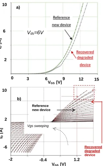
2.3 Characteristics of partially recovered device
The device was then characterized with the same SMU for re-using. Fig. 5a) shows the transfer characteristics at VDS = 6 V,
comparing a new device and the recovered device from Fig. 4c). For illustration, at VGS=12 V, the comparison shows a decrease
of only 20 % in ID for the recovered device. The same behaviour
is visible in Fig. 5b) on the output characteristics, which proves the potential re-usability of the device.
3. Structural characterisation and partial recovered device operation
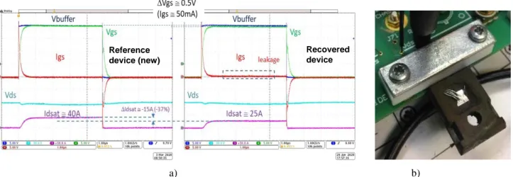
The plastic case of the device was opened by laser ablation followed by terminal chemical etching on the encapsulation resin. Fig. 6 a) shows the degraded die, with a very clear indication of severe damage to the top metal having accumulated in the proximity of the external gate-ring source-metal structural boundary. Lock-in-thermography analysis was also carried out, Fig. 6 b), which confirmed the abnormal heating of the cracked gate fingers around the corner region, where mechanical stresses are likely to be highest during the short-circuit. After opening, the device was re-used within a circuit, at reduced drain-source bias, and it was still able of correct transient operation, as demonstrated by the results in Fig. 7, which refer to a single short-circuit pulse. It can be seen that the channel saturation current is reduced of 37 % after the recovery gate-source process described above, as a result of the lowering of the IDS(VGS) curve
presented in Fig. 5 a).
4. Conclusion
The possibility to implement self-healing capability, remindful of film capacitor behaviour, in SiC power MOSFETs by ad hoc design and biasing is a new and very appealing feature, which can greatly change the present way to look at semiconductor device and power converter robustness, reliability and availability in application. This paper has shown that, following short circuit ageing stress and damage
Recovered degraded device Fig. 5 Transfer and direct behaviour comparison @ TCASE =
25 °C : a) IDS(VGS) @VDS = 6 V, b) IDS(VDS) curve. Reference new device Recovered degraded device Vgs sweeping
V
ds=6V
a) b)Fig. 6 a) Photograph of degraded device chip featuring damage accumulation at the boundary between gate-ring and source metal, b) LIT analysis @VGS = 10 V, IGSS = 10 mA, IDS = 1 A – 25 Hz.
source
gate
damage
VGS [V] 6 0 3 9 12 15 a) b) VGS [V] -2 -0.4 1.2 ID [A ] 10 6 2 ID [A ] 10 2 -6edge
accumulation, it is still possible to partially restore the integrity of the gate structure by proper electrical biasing for a particular class of devices and contained stress and damage levels. Here, device recovery was implemented in an off-line setup by means of a simple pulsed mode source-meter-unit, by progressively increasing the gate current limit. This operation is only possible if the gate is not already damaged too severely. In addition, it was shown that the voltage and injected recovery energy should be high enough to eliminate the main ohmic paths to be used at nominal gate voltage, but not so high as to cause excessive metal diffusion within the cracked oxide, which would yield a permanent short-circuit between the control terminals. Further studies are being dedicated to the online implementation of the recovery capability in a real power conversion system.
5. References
[1] A. Castellazzi et al., SiC power MOSFETs performance,
robustness and technology maturity, Microelectronics
Reliability (58) 2016, 164-176.
[2] F. Boige et al., Ensure an original and safe “fail-to-open”
mode in planar and trench power SiC MOSFET devices in
extreme short-circuit operation, Microelectronics
Reliability (88–90) 2018, 598-603.
[3] C. Chen et al., Study of short-circuit robustness of SiC
MOSFETs, analysis of the failure modes and comparison with BJTs, Microelectronics Reliability (55) 2015 1708–
1713.
[4] A. Romano et al, Influence of design parameters on the
short-circuit ruggedness of SiC power MOSFETs, in Proc.
ISPSD2015, May 2015, Hong Kong, China.
[5] F. Boige et al., Short-circuit robustness of parallel SiC
MOSFETs and fail-safe mode strategy, in Proc. EPE 2019,
Sep. 2019, Genoa, Italy.
[6] A. Fayyaz et al., Aging and failure mechanisms of SiC Power
MOSFETs under repetitive short-circuit pulses of different duration, in Proc. ICSCRM2019, Sep. 2019, Kyoto, Japan.
[7] F. Richardeau et al., SiC MOSFETs soft and hard failure
modes: functional analysis and structural characterization,
in Proc. ISPSD2020 – to be presented
[8] F. Boige, F. Richardeau, S. Lefebvre, M. Cousineau, SiC
power MOSFET in short-circuit operation: Electro-thermal macro-modelling combining physical and numerical approaches with circuit-type implementation, Mathematics
and Computers in Simulation,Volume 158, 2019, 375 - 386. [9] F. Richardeau, F. Boige, Circuit-type modelling of SiC power
Mosfet in short-circuit operation including selective fail-to-open and fail-to-short modes competition, Microelectronics
Reliability, Volumes 100–101, 2019.
[10] J. Liu, G. Zhang, B. Wang, W. Li and J. Wang, Gate Failure
Physics of SiC MOSFETs Under Short-Circuit Stress, in
IEEE Electron Device Letters, vol. 41, no. 1, pp. 103-106, Jan. 2020.
a) b)
Fig. 7 Single-pulse short-circuit test (VDS =100 V; VGS = 15 V, RGATE= 10
, TCASE = 25 °C): a), comparison of new reference device (left) and degradation-recovered device (right); b), photograph of recovered device in partly decapsulated TO247 package.Reference device (new)
Recovered device