HAL Id: hal-02974151
https://hal.laas.fr/hal-02974151
Submitted on 21 Oct 2020
HAL is a multi-disciplinary open access archive for the deposit and dissemination of sci-entific research documents, whether they are pub-lished or not. The documents may come from teaching and research institutions in France or abroad, or from public or private research centers.
L’archive ouverte pluridisciplinaire HAL, est destinée au dépôt et à la diffusion de documents scientifiques de niveau recherche, publiés ou non, émanant des établissements d’enseignement et de recherche français ou étrangers, des laboratoires publics ou privés.
Copyright
Denis Lagrange, Nicolas Mauran, Lucien Schwab, Bernard Legrand
To cite this version:
Denis Lagrange, Nicolas Mauran, Lucien Schwab, Bernard Legrand. Low Latency Demodulation for High-Frequency Atomic Force Microscopy Probes. IEEE Transactions on Control Systems Technol-ogy, Institute of Electrical and Electronics Engineers, In press, �10.1109/TCST.2020.3028737�. �hal-02974151�
Abstract—One prerequisite for high-speed imaging in dynamic-mode atomic force microscopy (AFM) is a fast demodulation of the probe signal. In this contribution, we present an amplitude and phase estimation method based on the acquisition of four points per oscillation, the sampling frequency being phase-locked on the probe actuation. The method is implemented on a RedPitaya platform, its clock being generated from the actuation signal of the probe. Experimental characterizations using square-modulated sine waves show that a latency of 500 ns is achieved with a carrier frequency of 10 MHz, which is 10-times faster compared to a state-of-the-art lock-in amplifier. A tracking bandwidth greater than 200 kHz is obtained experimentally. The method is eventually applied to a close-loop AFM scan realized using a 15-MHz AFM probe, showing its suitability for high-frequency oscillating probes.
Index Terms—Atomic force microscopy (AFM), field-programmable gate array (FPGA) implementation, amplitude and phase demodulation.
I. INTRODUCTION
TOMIC Force Microscopy (AFM) counts among the most important instrumental breakthroughs of the last century [1]. AFM has been at the origin of, and constantly supported the development of nanosciences, micro-nanotechnologies and nanobiology by providing not only sample topography down to the atomic scale [2] but also valuable spectroscopic information [3]. The dynamic modes of AFM, including non-contact and intermittent-non-contact modes [4,5], are often preferred to contact mode. They are less damaging for the tip and the sample and thus well-suited for the study of delicate samples like biological materials that would be altered by large interaction forces otherwise [6]. In the dynamic modes, the AFM probe tip is driven in oscillation close to the mechanical resonance frequency of the probe. Any interaction force between the oscillating tip and the sample surface translates into a change in amplitude, phase and eigenfrequency. The detection of the modulation allows retrieving the interaction information and obtaining the sample topography when supplied to a feedback system controlling the tip-to-surface distance [7]. In particular, high-speed imaging has received a lot of attention in recent years, motivated by the direct observation of fast biomolecular Manuscript submitted September 26, 2019. This work was supported by the French National Research Agency (ANR) under the research project OLYMPIA, grant ANR-14-CE26-001. L. Schwab was partly supported by the French DGA.
D. Lagrange, N. Mauran, L. Schwab and B. Legrand are with Laboratoire d’Analyse et d’Architecture des Systèmes (LAAS), CNRS UPR 8001, Université de Toulouse, 7 avenue du Colonel Roche, Toulouse, France. (e-mail: [email protected], [email protected], [email protected], [email protected]).
processes [8,9]. This purpose imposes constraints on the speed of the AFM feedback loop, which in return has motivated several works on the low-latency and high-bandwidth demodulation of the probe oscillation. Indeed, any delay introduced in the open-loop chain consisting of the probe, the demodulator and the z-axis actuator is detrimental to the AFM tracking bandwidth. Ruppert et al. have carried out a comprehensive review of these techniques [10]. They encompass mixing (synchronous) methods derived from the lock-in amplifier (LIA) operation [11,12], rectification (non-synchronous) methods such as rms-to-dc conversion and peak-hold detection [8,13], and amplitude and phase estimators using Kalman and Lyapunov filters [14,15]. Efforts have been put to digital implementations able to yield demodulation within one oscillation cycle or less for the sake of the tracking bandwidth [16,17]. It is worth noting that the methods have been mostly applied to AFM cantilevers with resonance frequencies up to a few hundreds of kHz, leading to bandwidth of a few tens of kHz. More data are given in Table I in the appendix.
Besides that, novel concepts of AFM probes have been developed these last years. They offer resonance frequencies greater than 10 MHz, even reaching 100 MHz recently, that is to say 2 orders of magnitude higher than that of usual AFM cantilevers [18-21]. They exploit resonating devices inherited from micro-electromechanical systems (MEMS) technology [18-20] and most advanced developments propose optomechanical transduction schemes [21]. The purpose is to push further the imaging speed of AFM and to enhance the resolution. Indeed, higher frequencies comes along with reduced oscillation amplitudes down to a few picometers [19,21], thus allowing operation in the short-range regime of forces where chemical interactions give substantial contributions to the AFM signal [22]. They also give access to spectroscopic experiments at the microsecond and below, paving the way to the nanosecond timescale that is unexplored yet but of utmost importance to confront experimental data to molecular dynamics simulations for example [23].
These high-frequency oscillating probes require a demodulator working above 10 MHz, a frequency greater than the one usually met in AFM applications. Moreover, considering an imaging rate of 100 kSa/s, which corresponds to 10 frames of 100 pixels ´ 100 pixels per second, the AFM bandwidth is 200 kHz. These figures show that the probe frequency is hundred times greater than the tracking bandwidth. It means that the oscillation period, lower than 100 ns, does not set a significant limitation in terms of latency to achieve the desired AFM tracking bandwidth, lifting in
Low Latency Demodulation for High-Frequency
Atomic Force Microscopy Probes
Denis Lagrange, Nicolas Mauran, Lucien Schwab, and Bernard Legrand
cycle. However, the delay introduced by the data numerical processing may be limitative in this frequency range. This is notably the case of LIAs that feature a demodulation latency of a few microseconds (See Table I in the appendix).
In this contribution, we propose a demodulation method based on the acquisition of only 4 samples per cycle, suitable for high-frequency AFM probes. The key point lies in using the frequency of the probe actuation signal as the reference for the automatic calculation of the sampling frequency by a multiplication b 4. This approach reduces the speed constraint in terms of sampling rate undergone by most of single-cycle methods, thus allowing the use of high-resolution ADC and ease of implementation. A cost-effective hardware based on a field-programmable gate array (FPGA) is employed for demonstration experiments. In the remainder of the article, experimental results are presented. They highlight the amplitude and phase estimation and the demodulation latency obtained for carrier frequencies ranging from 5 to 25 MHz. The method is then applied to AFM imaging using a 15-MHz probe.
II. PROBLEM FORMULATION OF AMPLITUDE AND PHASE ESTIMATION FOR HIGH FREQUENCY PROBES
We consider the measurement signal of the AFM probe tip vibration as an amplitude- and phase-modulated cosine wave:
𝑦(𝑡) = 𝑎(𝑡) cos*𝜔!𝑡 + 𝜙(𝑡). , (1)
where 𝜔! is the known angular frequency which the probe
oscillates at, 𝑎(𝑡) and 𝜙(𝑡) the time-varying amplitude and phase of the tip vibration induced by the tip-to-surface interaction during AFM operation. Taking into account the high frequency of the probe, e.g. 10 MHz, and a typical tracking bandwidth of 200 kHz, the amplitude and phase signals 𝑎(𝑡) and 𝜙(𝑡) vary very slowly with respect to the timescale of the carrier cycle. In particular, if one assumes a sine amplitude (or phase) modulation at angular frequency 𝜔", it means that 𝜔"≪ 𝜔!. Generally, amplitude modulation
index 𝛼 is much smaller than 1 when imaging using dynamic modes of AFM and 𝑎(𝑡) can be considered as a strictly positive value. The problem of amplitude and phase demodulation consists in estimating 𝑎(𝑡) and 𝜙(𝑡) from the measurement signal 𝑦(𝑡).
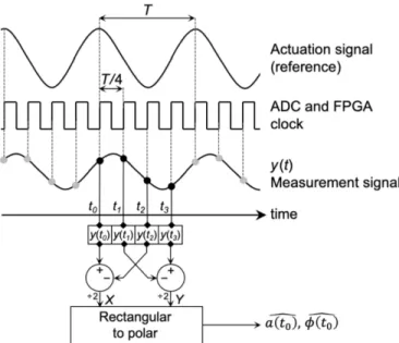
III. PRINCIPLE OF AMPLITUDE AND PHASE ESTIMATION The method we propose here relies on the acquisition of exactly four samples per cycle of the measurement signal 𝑦(𝑡). Practically, this is made possible by automatically generating the FPGA and sampling clock from the AFM probe actuation signal, the clock generation circuit providing a multiplication factor of 4. The principle of operation is illustrated in Fig. 1. Details of implementation will be given in Section IV. Basically, 4 data samples noted 𝑦(𝑡#) with i from 0 to 3 are used to estimate the amplitude and phase of
𝑦(𝑡) at time 𝑡!, where 𝑡!= 𝑛𝑇 and 𝑡#= 𝑡!+ 𝑖 𝑇 4⁄ . 𝑇 =
1 𝜔⁄ is the carrier cycle period and n is an integer. !
Fig. 1 Diagram of the principle of operation of the demodulation method. The AFM probe actuation signal acts as the reference signal to generate the FPGA and sampling clock by using a frequency multiplier by 4. 4 points y(ti)
of the measurement signal are sampled at ti = t0 + iT/4. They are used to
calculate X and Y, leading to the amplitude and phase estimates 𝑎(𝑡% and !)
𝜙(𝑡% by a rectangular-to-polar conversion. !)
An estimate of the amplitude 𝑎(𝑡8 and phase 𝜙(𝑡!) 8 is then !)
obtained by calculating: 𝑎(𝑡8 = √𝑋!) $+ 𝑌$ (2) and 𝜙(𝑡8 = arctan2(𝑌 𝑋!) ⁄ ) , (3) where 𝑋 =𝑦%𝑡0&−𝑦2 %𝑡2& , (4) 𝑌 =𝑦%𝑡3&−𝑦2 %𝑡1& , (5) and arctan2(x) is the four-quadrant inverse tangent function. Calculations for amplitude and phase estimation can be performed once the fourth sample is acquired at 𝑡 = 𝑡', that is
to say less than one carrier cycle period after 𝑡!, yielding
low-latency demodulation. It is worth noting that the differential calculations in (4) and (5) cancels out any dc offset affecting the measurement signal 𝑦(𝑡).
A. Steady State
In steady state conditions where 𝑎(𝑡) and 𝜙(𝑡) have constant values 𝑎 and 𝜙 respectively, (4) and (5) are straightforwardly re-written using (1) as: 𝑋 = 𝑎 cos 𝜙 and 𝑌 = 𝑎 sin 𝜙. This leads to 𝑎(𝑡8 = 𝑎 and 𝜙(𝑡!) 8 = 𝜙, i.e. an !)
errorless determination of the amplitude and phase of the signal.
B. Slowly Varying Amplitude and Phase
For slowly varying amplitude and phase with respect to the timescale of the carrier period T, a first order approximation is used to describe the behavior of 𝑎(𝑡) and 𝜙(𝑡) at 𝑡#= 𝑡!+
𝑎(𝑡#) ≈ 𝑎(𝑡!) + 𝑎̇(𝑡!) × 𝑖 𝑇 4⁄ , (6)
𝜙(𝑡#) ≈ 𝜙(𝑡!) + 𝜙̇(𝑡!) × 𝑖 𝑇 4⁄ . (7)
Using (1), (4), (5), (6) and (7), X and Y are then approximated to the first order as:
𝑋 ≈ [𝑎(𝑡!) + 𝑎̇(𝑡!) 𝑇 4⁄ ] cos 𝜙(𝑡!)
−H𝑎(𝑡!)𝜙̇(𝑡!) 𝑇 4⁄ I sin 𝜙(𝑡!) , (8)
𝑌 ≈ [𝑎(𝑡!) + 𝑎̇(𝑡!) 𝑇 2⁄ ] sin 𝜙(𝑡!)
+H𝑎(𝑡!)𝜙̇(𝑡!) 𝑇 2⁄ I cos 𝜙(𝑡!) . (9)
In the following sections III.C and III.D we calculate the amplitude and phase estimates 𝑎(𝑡8 and 𝜙(𝑡!) 8 in the case of !)
amplitude-modulated and phase-modulated signals, respectively.
C. Amplitude Modulation
Amplitude-modulated signals are defined for 𝜙(𝑡) = 𝜙 and 𝜙̇(𝑡) = 0. Using this consideration and first-order calculation, we obtain from (2), (3), (8) and (9):
𝑎(𝑡8 ≈ 𝑎(𝑡!) !) K1 +()̇(,.)(,!) !)(3 − cos 2𝜙)M (10) and 𝜙(𝑡8 ≈ 𝜙 +!) ()̇(,! ) .)(,!)sin 2𝜙 . (11)
Equation (10) shows that in the worst case, the relative error on the estimated amplitude reaches ()̇(,!)
$)(,!) . Considering a
slowly varying signals as we assumed in Section II, this value is much lower than 1. In particular, for a sine amplitude modulation, the estimation error remains lower than /0"
$0! , i.e.
lower than 10-3 in the case of a 10-MHz AFM probe
frequency, a 200-kHz modulation frequency, and a modulation index 𝛼 = 0.1 . As for the phase estimate (11), the error reaches ()̇(,!)
.)(,!) in the worst case, i.e. it remains lower than /0"
.0!,
which is of the order of 10-4 radians for the sine amplitude
modulation given just above as an example.
D. Phase Modulation
Phase-modulated signals correspond to 𝑎(𝑡) = 𝑎 and 𝑎̇(𝑡) = 0. Using this consideration, we obtain:
𝑎(𝑡8 ≈ 𝑎 K1 +!) (1̇(,! ) . sin 2𝜙M (12) and 𝜙(𝑡8 ≈ 𝜙(𝑡!) !) +(1̇(,! ) . (3 + cos 2𝜙) . (13)
Equations (12) and (13) show that the estimation errors are ruled by 𝑇𝜙̇(𝑡!) that is much lower than 1 for a slowly
varying phase-modulated signals. In the case of a sine phase modulation with a 10-MHz AFM probe frequency, a 200-kHz modulation frequency, and a phase deviation 𝛽 = 0.1 rad, estimation errors remain lower than 20"
0! ~2. 10 3'.
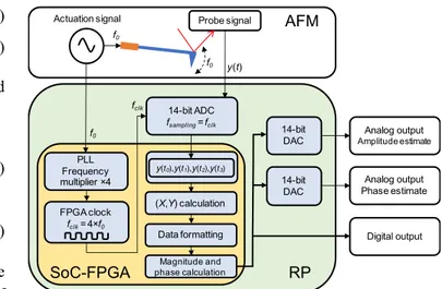
Fig. 2 Block diagram of the implementation of the method on the RedPitaya platform (RP). The PLL included in the FPGA generates the clock frequency fclk by multiplying the actuation signal frequency f0 by 4. ADC samples of the
measurement signal y(t) are acquired at fsampling = fclk and stored in registers.
Once four signal samples are available the calculation of X and Y is performed. Values are then formatted and converted to magnitude and phase. Estimates are finally output thanks to the DACs.
IV. IMPLEMENTATION DETAILS
The estimation method was implemented on a RedPitaya STEMlab 125-14 platform (RP) featuring a Xilinx Zynq 7010 system-on-chip (SoC), a dual-channel 14-bit analog-to-digital converter (ADC), and a dual-channel 14-bit digital-to-analog converter (DAC) [24]. A phase-locked loop (PLL) implemented on the FPGA of the SoC was used to generate the FPGA clock fclk from the AFM actuation signal. The PLL multiplier was set so that fclk was 4 times the frequency of the reference f0. The sampling clock of the ADC is locked to fclk, thus allowing the acquisition of exactly 4 ADC samples of the measurement signal per period T. Note that the clock generation of the RP were studied elsewhere in terms of phase noise and frequency stability, underlining its suitability for most time and frequency applications [25]. The ADC input and DAC outputs were configured with a range of ±1 V.
A block diagram of the main components implemented on the RP is shown in Fig. 2. The latency of the whole demodulation process has been estimated to 16 FPGA clock cycles, i.e. 4 periods of the measurement signal y(t).
V. EXPERIMENTAL RESULTS
A. Square Amplitude Modulation
A test bench was set up to validate the method implemented on the RP, consisting of a dual-channel function generator to produce the reference signal and a square amplitude-modulated sine signal. The carrier frequency chosen was 𝑓!=
𝜔!⁄2𝜋= 10 MHz, which is of the order of magnitude of the
resonance frequency of AFM Ring Probes from Vmicro [19,26]. A Zurich Instruments HF2LI lock-in amplifier (ZI LIA) was used as a reference for performance comparison. The ZI LIA input range was set to ±1 V. The cutoff frequency of its post-mixing low-pass filter was set to 200 kHz, i.e. the highest selectable value.
14-bit ADC fsampling= fclk Actuation signal Probe signal
14-bit DAC 14-bit DAC Analog output Amplitude estimate Analog output Phase estimate Digital output y(t) f0 f0 f0 AFM PLL Frequency multiplier ×4 FPGA clock fclk= 4×f0 y(t0),y(t1),y(t2),y(t3) (X,Y) calculation Data formatting Magnitude and phase calculation RP fclk SoC-FPGA
Fig. 3 (a) 10-MHz carrier sine wave amplitude-modulated by a square wave with fm = 10 kHz. (b) Amplitude estimate from the RedPitaya platform.
(c) Demodulated amplitude signal with the ZI LIA.
Fig. 4 (a) 10-MHz carrier sine wave amplitude-modulated by a square wave with fm = 10 kHz. (b) Amplitude estimate from the RedPitaya platform.
(c) Demodulated amplitude signal with the ZI LIA. (d), (e) and (f): Close-view of (a), (b) and (c) respectively, from 0 to 1 microsecond.
The reference and modulated signals were simultaneously applied to the RedPitaya platform (RP) and the ZI LIA inputs through 50-ohm power splitters. Analog outputs as well as the modulated signal were recorded using a four-channel digital oscilloscope.
Time responses of RP and ZI LIA amplitude outputs RRP and RLIA are plotted in Fig. 3 for a square amplitude modulation. 10000 data points were acquired for each channel. It can be seen in Fig. 3b that the RP delivers a faster output than the one of the ZI LIA, which is delayed with a noticeable rise time (Fig. 3c). In Fig. 4, we show a closer view where it can be observed in Fig. 4b and 4e that the estimation latency is about 0.5 µs for the RP whereas the ZI LIA signal starts rising after ~5 µs (Fig. 4c). Moreover, the steady-state value of amplitude output is reached in ~100 ns for the RP estimation, a significantly shorter value than the ~3 µs required by the ZI LIA. Note that this longer transient time is ruled by the post-mixing filter of the ZI LIA that also explains a slightly better noise rejection.
Fig. 5 (a) 10-MHz carrier sine wave phase-modulated by a square wave with fm = 10 kHz and a 90-degree phase shift. (b) Phase estimate from the
RedPitaya platform. (c) Demodulated phase signal with the ZI LIA.
Fig. 6 (a) 10-MHz carrier sine wave phase-modulated by a square wave with fm = 10 kHz and a 90-degree phase shift. (b) Phase estimate from the
RedPitaya platform. (c) Demodulated phase signal with the ZI LIA. (d), (e) and (f): Close-view of (a), (b) and (c) respectively, from 0 to 1 microsecond.
B. Square Phase Modulation
The same test bench and experimental conditions as in the previous section were employed to study the time responses of the RP and ZI LIA phase outputs 𝜙RP and 𝜙LIA to a 90-degree square phase modulation. Data are plotted in Fig. 5 and 6 for the sake of a comparison. As it can be observed, the same analysis as for amplitude modulation applies to phase modulation: the RP achieved phase estimation with a latency of ~0.5 µs whereas it is delayed by about 6 µs for the ZI LIA. Steady-state values of phase estimations are reached in about 120 ns and ~3 µs for the RP and the ZI LIA, respectively.
C. Demodulation Latency
The two previous sections have evidenced that the proposed method implemented on the RP is able to detect and output a change in the amplitude or in the phase of a 10-MHz signal with a delay shorter by one order of magnitude compared with the ZI LIA. To go further in the analysis, we studied the latency of the responses as a function of the frequency of the
-1 0 (c) (b) In pu t s ig na l ( 0.0 0.1 0.2 0.3 RR P ( V ) 0 50 100 150 200 0.0 0.2 0.4 0.6 0.8 RL IA ( V ) Time (µs) RedPitaya estimate ZI LIA estimate -1 0 1 (c) (b) In pu t s ig na l ( V ) (a) -1 0 1 (d) 0.0 0.1 0.2 0.3 RR P ( V ) 0.0 0.1 0.2 0.3 (e) -2 0 2 4 6 8 10 0.0 0.2 0.4 0.6 0.8 RLIA ( V ) Time (µs) (f) 0.0 0.5 1.00.0 0.2 0.4 0.6 0.8 Time (µs) ZI LIA estimate RedPitaya estimate -2 -1 0 1 (c) (b) In pu t s ig na l ( -0.5 0.0 0.5 !RP ( V ) 0 50 100 150 200 -1 0 1 !LIA ( V ) Time (µs) RedPitaya estimate ZI LIA estimate -2 -1 0 1 2 (c) (b) In pu t s ig na l ( V ) (a) -2 -1 0 1 2 (d) -0.5 0.0 0.5 !RP ( V ) -0.5 0.0 0.5 (e) -2 0 2 4 6 8 10 12 14 -1 0 1 !LIA ( V ) Time (µs) (f) 0.0 0.5 1.0 -1 0 1 Time (µs) RedPitaya estimate ZI LIA estimate
carrier signal f0. In the following, the latency is defined as the delay required to reach half of the steady-state response after a change in the modulated signal. The measurement results are given in Fig. 7. The range f0 from 5 to 25 MHz is studied, the upper value being limited by the maximum clock frequency
fclk supported by the RP. In the case of the ZI LIA, the latency appears to be independent of the carrier frequency, with an average of 6.46 µs for amplitude demodulation and 7.10 µs for phase demodulation. These values are in good agreement with the specifications of the instrument giving a lag time of 7 to 10 µs. On the contrary, the RP features a latency that decreases from 875 ns to 225 ns as the carrier frequency f0 increases from 5 to 25 MHz. More in details, the latency-versus-frequency plot fits a hyperbolic law given by 𝜏 = 75 + 44!5#
!, where 𝜏 is the latency in nanoseconds. 𝜏 can be
re-written as 𝜏 = 75 + 4𝑇Z, where 𝑇Z is the carrier period in nanoseconds. This law is in very good agreement with what expected by the implementation described in Section IV. 16 system-clock cycles corresponding to 4 carrier periods are indeed required by the RedPitaya platform to perform the estimation: the higher the carrier frequency, the higher the system-clock frequency and the shorter the processing time. A constant delay of 75 ns adds up to this processing time that we attribute to transmission delay in cables and to electrical delay of the analog input and output amplifiers of the RedPitaya platform.
D. Sine Amplitude and Phase Modulations
A second test bench was set up to study the frequency response of the RP to sine amplitude- and phase-modulated signals. It consisted of a Zurich Instruments HF2LI LIA with multi-frequency and modulation options that produced the reference signal and the modulated signals applied to the RP. The carrier frequency and peak amplitude were chosen to be 𝑓!= 𝜔!⁄2𝜋= 10 MHz and 500 mV, respectively. We varied
the modulation frequency 𝑓"= 𝜔"⁄ from 1 kHz to 1 MHz. 2𝜋
Fig. 7 Latency of the amplitude output (squares) and phase output (circles) versus the carrier frequency f0 for the RP (in red) and ZI LIA (in blue). Error
bars correspond to a measurement uncertainty of half a carrier period. Dashed lines are plotted as guides for the eye. In the case of the RP latency, it corresponds to a hyperbolic fit. The ZI LIA post-mixing low-pass filter is set at its maximum cutoff frequency of 200 kHz.
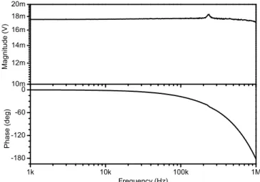
Fig. 8 Frequency response of the amplitude output of the RP to an amplitude-modulated input with a carrier frequency f0 = 10 MHz.
Fig. 9 Frequency response of the phase output of the RP to a phase-modulated input with a carrier frequency f0 = 10 MHz.
Modulation index was set to 0.1. The analog outputs for amplitude and phase estimates from the RP were synchronously demodulated at frequency 𝑓" by the ZI LIA.
Figure 8 presents the frequency response to an amplitude modulation. Results show that the magnitude response of the amplitude estimate of the RP is flat over a 200 kHz bandwidth, which is consistent with the calculations in Section III. It decreases perceptibly as the modulation frequency 𝑓" is
increased up to 1 MHz, featuring however a slight bump around 𝑓"= 250 kHz that we have no evident explanation
for. As for the phase response of the amplitude estimate, it decreases regularly with the modulation frequency 𝑓". This is
explained by the latency 𝜏 ≈ 500 ns of the RP at the carrier frequency 𝑓!= 10 MHz that causes a drift of the phase
response proportional to the modulation frequency 𝑓". The
frequency response to a phase modulation is shown in Fig. 9. The phase estimate of the RP behaves similarly to the amplitude estimate in Fig. 8 and the same analysis applies.
E. Measurement Resolution
The measurement resolution is defined by the smallest amplitude or phase change in the input signal that can be detected and translated into a voltage change at the analog outputs of the RP. The 14-bit DACs combined with the ±1 V
0 5 10 15 20 25 30 0.0 0.2 0.4 0.6 0.8 1.0 6.2 6.4 6.6 6.8 7.0 7.2 L a te n cy ( µ s ) Frequency (MHz) RRP !RP RLIA !LIA ZI LIA latency RedPitaya latency 1k 10k 100k 1M -180 -120 -60 0 P h a se ( d e g ) Frequency (Hz) 10m 12m 14m 16m 18m 20m M a g n itu d e ( V ) 1k 10k 100k 1M -180 -120 -60 0 P h a se ( d e g ) Frequency (Hz) 10m 12m 14m 16m 18m 20m M a g n itu d e ( V )
which corresponds also to the minimum voltage change we were able to observe with the oscilloscope. This being taken into consideration, we first checked that the amplitude estimate varied linearly with the input signal amplitude up to 1.5 Vpp and we determined that the minimum detectable
change in the input signal amplitude was 0.5 mVpp,
corresponding to a 120-µV change in the amplitude estimate output signal. Given the ±1 V input range of the ADC of the RP, this yielded a 72-dB dynamic reserve. We performed similar experiments to determine the phase resolution of the RP. We obtained an experimental resolution of 0.2 degree, the full-scale of the phase measurement being 360 degrees. This phase resolution value was achieved for an input signal amplitude ranging from 50 mVpp to 1.5 Vpp.
F. Sensitivity to noise
In the previous experiments, signals were provided by a function generator. In an AFM application, the probe oscillation signal would have some superimposed noise. In order to investigate the sensitivity of our demodulation method to noise, we analyzed the amplitude output of the RP when the frequency of a small signal acting as an added noise is swept and applied to the input. In the measurement plotted in Fig. 10, the demodulator frequency is fixed to 10 MHz. As one can expect, we observe that the noise sensitivity is maximal at the demodulation frequency. For lower frequencies the noise sensitivity decreases monotonically. It theoretically tends to 0 at dc as expected from the differential calculations (see Section III for details of the method). Nodes in the sensitivity response for even harmonics of the demodulation frequency are explained similarly. On the contrary, maxima of noise sensitivity occur for odd harmonics, which is understood as an aliasing effect in relation to the sampling frequency of the RP. The sensitivity to noise is obviously higher than for other synchronous methods making use of 10-20 samples per period typically, which offers some level of filtering and greater noise rejection. The main drawback of our method lies in its poor noise rejection at the frequencies of odd harmonics of the carrier signal.
Fig. 10 Noise sensitivity versus frequency of the demodulation method obtained from the response to a sine small signal swept from 2 to 50 MHz. The demodulation frequency f0 of the RedPitaya platform is set to 10 MHz in
the experiment.
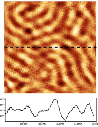
Fig. 11 AFM image of a block copolymer sample surface obtained using the proposed demodulation method implemented on the RedPitaya platform. Scan size: 490 nm ´ 490 nm (200 pix. ´ 200 pix.). Acquisition time: 4 s. The dashed line in the AFM image indicated the location of the cross-section.
G. AFM imaging
The demodulation method implemented on the RP was used in a dynamic mode AFM experiment so as to demonstrate its functionality and suitability in a real case application. A homemade AFM microscope was used for the experiment, which consists of a XYZ PicocubeTM piézo scanner (P-363 /
E-536, Physik Instruments) and a controller based on a CompactRIO 9035 system (National Instruments). The AFM probe was a Ring Probe (Vmicro) with resonance frequency of 𝑓!≈ 15.86 MHz and quality factor of about 200 [26]. This
high-frequency probe based on MEMS technologies integrates capacitive electromechanical transducers for driving and sensing the tip oscillation. Further details of the probe operation are given in Ref. [19]. We used amplitude-modulation mode AFM. The setpoint was set to 99 % of the free-air amplitude estimated to be 50 pm. A block copolymer sample was scanned and Fig. 11 shows the image. A lamellar structure is observed, corresponding to the stiffness contrast of the hard and soft self-structured domains of the copolymer material. This result should be compared with those of Ref. [19], obtained on a similar material yet using a LIA demodulation, and showing that the image quality is identical.
VI. CONCLUSION
We have introduced in this article a fast amplitude and phase estimation method designed for high-frequency atomic force microscopy probes. One key feature is the low latency achieved thanks to a short signal-acquisition and data-processing time. We implemented the method on a RedPitaya
1M 10M 100M -20 -15 -10 -5 0 Frequency (Hz) N o is e s e n si tiv ity ( d B ) 100nn 200nn 300nn 400nn 500nn 2nm 4nm 6nm 8nm
STEMlab 125-14 platform. We demonstrated a 500-ns demodulation latency at 10-MHz carrier frequency (225 ns at 25 MHz), a value smaller by one order of magnitude compared to state-of-the-art methods working in the same frequency range. This low latency is essential to extend the tracking bandwidth of the AFM beyond 100 kHz, i.e. for speed imaging in close-loop configuration with high-frequency probes. Other characterizations have highlighted the bandwidth in response to amplitude- and phase-modulated signals as well as the resolution and the noise sensitivity. The authors believe that this estimation method will be useful for high-speed AFM exploiting high-frequency probes recently appeared in the literature, as a contribution to minimizing the time-delay associated with components in the microscope feedback loop. In this context, the AFM experiment using the proposed method demonstrates that the concept is functional for AFM imaging with a 15 MHz probe.
APPENDIX TABLEI
COMPARISON OF DEMODULATION METHODS USED IN AFM APPLICATIONS
Method Carrier frequency f0 (MHz) Demodulation latency (µs) Demodulation bandwidth (kHz) Reference Synchronous methods LIA ZI HF2LI ≤ 50 7 200 [27] LIA ZI UFHLI ≤ 600 3 5000 [27] Coherent demodulation 0.088 50 N/A [17] High-bandwidth LIA 0.1 N/A 40 [12]
Kalman filter 0.137 N/A ≈30 [14] Lyapunov filter 0.05 ≈5 50 [15] Proposed
method 5 to 25
0.5
(f0 = 10 MHz) 200 This work
Non synchronous methods RMS-to-DC ≤ 1 (f 5
0 = 1 MHz) 200 [8,28]
Peak-hold ≤ 1 (f 1
0 = 1 MHz) 250 [8,28]
REFERENCES
[1] G. Binnig, C.F. Quate, and C. Gerber, “Atomic force microscope.”, Phys. Rev. Lett., vol. 56, no. 9, pp. 930-933, 1986
[2] G. Binnig, C. Gerber, E. Stoll, T.R. Albrecht, and C.F. Quate, “Atomic resolution with atomic force microscope.”, Europhys. Lett., vol. 3, no. 12, pp. 1281-1286, 1987
[3] M.B. Viani, L.I. Pietrasanta, J.B. Thompson, A. Chand, I.C.
Gebeshuber, J.H. Kindt, M. Richter, H.G. Hansma, and P.K. Hansma, “Probing protein-protein interactions in real time.”, Nat. Struct. Biol., vol. 7, no. 8, pp. 644‐647, 2000
[4] T.R. Albrecht, P. Grütter, D. Horne, and D. Rugar, “Frequency modulation detection using high-Q cantilevers for enhanced force microscopy sensitivity.”, J. Appl. Phys., vol. 69, no. 2, pp. 668-673, 1991
[5] Q. Zhong, D. Inniss, K. Kjoller, and V.B. Elings, “Fractured polymer/silica fiber surface studied by tapping mode atomic force microscopy.”, Surf. Sci. Lett., vol. 290, no. 1, pp. 688-692, 1993
[6] C.A.J. Putman, K.O. van der Werf, B.G. de Grooth, N.F. van Hulst, and J. Greve, “Viscoelesticity of living cells allows high resolution imaging by tapping mode atomic force microscopy.”, Biophys. J., vol. 67, pp. 1749-1753, 1994
[7] G. Haugstad, “Overview of AFM.”, in Atomic Force Microscopy: Understanding Basic Modes and Advanced Applications, Hoboken, NJ, USA: John Wiley & Sons, 2012, ch. 1, pp. 1-32
[8] T. Ando, T. Uchihashi and T. Fukuma,, “High-speed atomic force microscopy for nano-visualization of dynamic biomolecular processes.”, Prog. Surf. Sci., vol. 83, no. 7-9, pp. 337-437, 2008
[9] N. Kodera, D. Yamamoto, R. Ishikawa and T. Ando, “Video imaging of walking myosin V by high-speed atomic force microscopy.”, Nature, vol. 468, no. 7320, pp. 72-76, 2010
[10] M.G. Ruppert, D.M. Harcombe, M.R.P. Ragazzon, S.O.R Moheimani, and A.J. Fleming, “A review of demodulation technique for amplitude-modulation atomic force microscopy.”, Beilstein J. Nanotechnol., vol. 8, pp. 1407-1426, 2017
[11] E.D. Morris and H.S. Johnston, “Digital phase sensitive detector” Rev. Sci. Instrum., vol. 39, pp. 620–621, 1968
[12] K.S. Karvinen and S.O.R. Moheimani, “A high-bandwidth amplitude estimation technique for dynamic mode atomic force microscopy.”, Rev. Sci. Instrum., vol. 85, 023707, 2014
[13] C. Kitchin and L. Counts, “RMS-DC conversion – theory”, in RMS to DC conversion application guide, 2nd ed., Analog Devices, 1986, ch. 1,
pp. 1-5. [Online]. Available: https://www.analog.com/en/education /education-library/rms-to-dc-application-guide.html
[14] M.G. Ruppert, K.S Karvinen, S.L. Wiggins, and S.O.R. Moheimani, “A Kalman filter for amplitude estimation in high-speed dynamic mode atomic force microscopy”, IEEE Trans. Control Syst. Technol., vol. 34, no. 1, pp. 276–284, 2016
[15] M.R.P. Ragazzon, M.G. Ruppert, D.M. Harcombe, A.J. Fleming, and J.T. Gravdahl, “Lyapunov Estimator for high-speed demodulation in dynamic mode atomic force microscopy”, IEEE Trans. Control Syst. Technol., vol. 26, no. 2, pp. 1-8, 2017
[16] D.Y. Abramovitch. (2011/06). “Low latency demodulation for Atomic Force Microscopes, Part I efficient real-time integration.”, presented at American Control Conference, IEEE, pp. 2252-2257. Available:
https://doi.org/10.1109/ACC.2011.5991144
[17] D.Y. Abramovitch, “Low latency demodulation for Atomic Force Microscopes, Part II: Efficient Calculation of Magnitude and Phase.”, IFAC Proceedings Volumes, vol. 44, no. 1, pp. 12721-12726, 2011 [18] E. Algré, Z. Xiong, M. Faucher, B. Walter, L. Buchaillot and B.
Legrand, “MEMS ring resonators for laserless AFM with sub-nanoNewton force resolution.”, J. of Microelectromech. Syst., vol. 21, pp. 385-397, 2012
[19] B. Legrand, J.-P. Salvetat, B. Walter, M. Faucher, D. Théron, and J.-P. Aimé, “Multi-MHz micro-electro-mechanical sensors for atomic force microscopy.”, Ultramicroscopy, vol. 175, pp. 46-57, 2017
[20] B. Walter, E. Mairiaux, and M. Faucher, “Atomic force microscope based on vertical silicon probes.”, Appl. Phys. Lett., vol. 110, no. 24, pp. 243101-1-243101-4, 2017
[21] P.E. Allain, L. Schwab, C. Misner, M. Gely, E. Mairiaux, M. Hermouet, B. Walter, G. Leo, S. Hentz, M. Faucher, G. Jourdan, B. Legrand, and I. Favero, “Optomechanical resonating probe for very high-speed sensing of atomic forces.”, Nanoscale, vol. 12, no. 5, pp. 2939-2945, 2020 [22] L. Gross, F. Mohn, N. Moll, P. Liljeroth, and G. Meyer, “The Chemical
Structure of a Molecule Resolved by Atomic Force Microscopy”, Science, vol. 325, pp. 1110-1114, 2009
[23] M. Sotomayor and K. Schulten, “Single-molecule experiments in vitro and in silico.”, Science, vol. 316, pp. 1144-1148, 2007
[24] RedPitatya STEMlab board. [Online]. Available: https://www.redpitaya.com/f130/STEMlab-board
[25] A.C. Cardenas Olaya, C.E. Calosso, J.M. Friedt, S. Micalizio, and E. Rubolia, “Phase Noise and Frequency Stability of the RedPitaya Internal PLL.”, IEEE Trans. Ultrason. Ferroelectr. Freq. Control, vol. 66, no. 2, pp. 412-416, 2019
[26] Vmicro Ring probe product. [Online]. Available: http://vmicro.fr/products/
[27] From the specifications of Zurich Instruments Lock-in Amplifiers products. [Online]. Available: http://www.zhinst.com
[28] T. Ando, N. Kodera, E. Takai, D. Maruyama, K. Saito, and A. Toda, “A high-speed atomic force microscope for studying biological macromolecules”, Proc. Natl. Acad. Sci. USA, vol. 98, no. 22, pp. 12468-12472, 2001
France. In 1981, he graduated in electro-technical engineering from ENSEEIHT in Toulouse, France.
He started his career at a research center of Renault, belonging to a team in charge of the development of electrical vehicles. Later, he extended his expertise in circuit and system design for demanding and critical applications, e.g. electron gun control circuits for particle accelerators, or on-board systems for the spaceborne infrared telescope Herschel. He joined the Laboratoire d'Analyse et d'Architecture des Systèmes (LAAS-CNRS) in 2001. He is currently involved in the development of several research projects, bringing his expertise in low-noise and high-bandwidth signal acquisition and processing for microelectronics, MEMS applications and scientific instrumentation.
Nicolas Mauran was born in Muret, France, in 1974. He received the engineering degree in instrumentation of the Conservatoire National des Arts et Métiers of Toulouse, France, in 2003. He joined the Laboratoire d'Analyse et d'Architecture des Systèmes (LAAS-CNRS) in 1996, where he is currently responsible for the platform dedicated to the characterization of electron devices. His expertise encompasses low- and high-power electrical characterizations, electrostatic discharge test methods and device failure analysis. He has developed and automated several experimental test benches, including high-speed and real-time architectures for scientific instrumentation.
nanosciences from PHELMA, a College of engineering based in Grenoble, France, in 2016.
His 6-months-internship to pass his diploma took place in LPA (Paris, France) with Gabriel Hétet. It concerned the manipulation of the spin of NV-centers in diamond. He is currently with the MEMS team of the LAAS-CNRS (Toulouse, France) as a Ph.D. student under Bernard Legrand’s supervision. The subject of his thesis focuses on the implementation of optomechanical probes on an atomic force microscope. He is particularly involved in the characterization of the devices and in proof-of-concept experiments.
Bernard Legrand received the electrical engineering degree and the M.S. degree in electronics in 1996, and the Ph.D. degree in electronics in 2000 from the Université des Sciences et Technologies de Lille, Villeneuve d’Ascq, France.
From 1996 to 2000, he was working on semiconductor nanostructures and was involved in their fabrication and characterization using techniques based on scanning probe microscopies. He was appointed a CNRS research scientist in 2001 and joined the Silicon Microsystems Group of IEMN, Lille, France. Since 2007, one of his research topics has concerned the development of high-frequency atomic force microscopy (AFM) probes based on micro-electromechanical systems (MEMS) technology, including more recently optomechanics as a sensing principle. Potential applications are foreseen in the field of high-speed microscopy and spectroscopy of nanobiosystems. In 2013, he moved to the LAAS-CNRS in Toulouse, France, where he is currently the head of the Micro Nano Bio Technologies department. He has served as a member of technical program committees of international conferences, including IEEE MEMS and IEEE IEDM, and as a member of the editorial board of the Elsevier Ultramicroscopy journal.