HAL Id: hal-01480614
https://hal.archives-ouvertes.fr/hal-01480614
Submitted on 1 Mar 2017
HAL is a multi-disciplinary open access
archive for the deposit and dissemination of
sci-entific research documents, whether they are
pub-lished or not. The documents may come from
L’archive ouverte pluridisciplinaire HAL, est
destinée au dépôt et à la diffusion de documents
scientifiques de niveau recherche, publiés ou non,
émanant des établissements d’enseignement et de
Memristor nanodevice for unconventional
computing:review and applications
Mahyar Shahsavari, Pierre Boulet
To cite this version:
Mahyar Shahsavari, Pierre Boulet. Memristor nanodevice for unconventional computing:review and
applications . [Research Report] Université de Lille 1, Sciences et Technologies; CRIStAL UMR 9189.
2016. �hal-01480614�
Memristor nanodevice for unconventional computing:
review and applications
Mahyar Shahsavari, Pierre Boulet
Univ. Lille, CNRS, Centrale Lille, UMR 9189 - CRIStAL
Centre de Recherche en Informatique Signal et Automatique de Lille,
Abstract
A memristor is a two-terminal nanodevice that its properties attract a wide community of re-searchers from various domains such as physics, chemistry, electronics, computer and neuroscience. The simple structure for manufacturing, small scalability, nonvolatility and potential of using in low power platforms are outstanding characteristics of this emerging nanodevice. In this report, we review a brief literature of memristor from mathematic model to the physical realization. We discuss different classes of memristors based on the material used for its manufacturing. The potential applications of memristor are presented and a wide domain of applications are explained and classified.
Contents
1 Introduction . . . 2
2 Memristor device overview and properties . . . 2
2.1 Memristor a missing electrical passive element . . . 3
2.2 Memristive device functionality . . . 4
2.3 Electrical model . . . 5
3 Memristor classification based on different materials and applications . . . 5
3.1 Resistive Memristor . . . 6
3.2 Spintronic Memristor . . . 7
3.3 Organic (Polymeric) Memristor . . . 8
3.4 Ferroelectric Memristor . . . 9
3.5 Evaluation of Memristor with different materials . . . 10
4 Potential applications of memristors . . . 11
4.1 Memristor-based nonvolatile memory . . . 11
4.2 Digital computing . . . 12
4.3 Analog domain applications . . . 12
5 Streams of research . . . 12
1
Introduction
Memristor has recently drawn the wide attention of scientists and researchers due to non-volatility, better alignment, and excellent scalability properties [1]. Memristor has initiated a novel research direction for the advancement of neuromorphic and neuro-inspired computing. Memristor remembers its last state after the last power plugging and has a simple physical structure, high-density integration, and low-power consumption. These features make the memristor an attractive candidate for building the next generation of memories [2]. In addition, from high-performance computing point of view, the memristor has the potential capability to conquer the memory bottleneck issue, by utilizing computational unit next to the memory [3]. Due to these unique properties and potentials of the memristor, neuroscientists and neuromorphic researchers apply it as an artificial synapse in Spiking Neural Network (SNN) architectures [4].
Memristor was predicted in 1971 by Leon Chua, a professor of electrical engineering at the University of California, Berkeley, as the fourth fundamental device [5]. Publishing a paper in the Nature journal by Hewlett Packard (HP) [6] in May 2008, announced the first ever experimental realization of the memristor, caused an extraordinary increased interest in this passive element. Based on the symmetry of the equations that govern the resistor, capacitor, and inductor, Chua hypothesized that fourth device should exist that holds a relationship between magnetic flux and charge. After the physical discovery of the memristor, several institutions have published the memristor device fabrications using a variety of different materials and device structures [6–10]. In 2009, Biolek et al. modeled nonlinear dopant drift memristor by SPICE [11]. One year later, Wei Lu, professor at the University of Michigan proposed a nanoscale memristor device which can mimic the synapse behavior in neuromorphic systems [12]. Later on, in 2011 a team of multidisciplinary researchers from Harvard University published an interesting paper on programmable nanowire circuits for using in nanoprocessors [13]. Until June 2016, based on the Scopus bibliographic database, 2466 papers have been published in peer-reviewed journals and ISI articles which are related to memristor fabrication or applications of the memristor in different Domains of science and technology.
Memristors are promising devices for a wide range of potential applications from digital memory, logic/analog circuits, and bio-inspired applications [14]. Especially because the nonvolatility property in many types of memristors,they could be a suitable candidate for making non-volatile memories with ultra large capacity [15]. In addition to non-volatility, the memristor has other attractive features such as simple physical structure, high-density, low-power, and unlimited endurance which make this device a proper choice for many applications. Different device structures are still being developed to determine which memristor device can be presented as the best choice for commercial use in memory/flash manufacturing or in neuromorphic platforms. This is based on different factors such as size, switching speed, power consumption, switching longevity, and CMOS compatibility. The rest of the manuscript is organized as follows: In Section 2, a general overview of the memristor is done and the electrical properties have been investigated. Section 3 presents memristor implementation and fabrication. We investigate various types of memristors based on the different materials that have been used in the fabrication. In Section 4, potential applications of Memristor has been studied. Section 5 deals with streams of research, we have investigated a research classification from the physics level to the system design. Finally, we describe a brief summary and the future work.
2
Memristor device overview and properties
In this section, we discuss the memristor nanodevice which is believed to be the fourth missing fundamental circuit element, that comes in the form of a passive two-terminal device. We discuss how it can remember its state, and what is its electrical model and particular properties.
Figure 1: Relations between the passive devices and the anticipating the place of the fourth fundamental element based on the relations between charge (q) and flux (ϕ) (from [6]).
2.1
Memristor a missing electrical passive element
Memristor is a contraction of “memory & resistor,” because the basic functionality of the memristor is to remember its state history. This characteristic proposes a promising component for next generation memory. Memristor is a thin-film electrical circuit element that changes its resistance depending on the total amount of charge that flows through the device. Chua proved that memristor behavior could not be duplicated by any circuit built using only the other three basic electronic elements (Resistor,Capacitor, Inductor), that is why the memristor is truly fundamental. As it is depicted in Figure 1, the resistor is constant factor between the voltage and current (dv = R.di), the capacitor is a constant factor between the charge and voltage (dq = C.dv), and the inductor is a constant factor between the flux and current (dϕ = L.di). The relation between flux and charge is Obviously missing (dϕ = M.dq) that can be interpreted by a fourth fundamental element such as memristor [5].
Obviously, in memristive devices, the nonlinear resistance can be changed and memorized by controlling the flow of the electrical charge or the magnetic flux. This control any two-terminal black box is called a memristor if, and only if, it exhibits a pinched hysteresis loop for all bipolar periodic input current signaling is interesting for the computation capability of a device similar to the controlling of the states of a transistor. For instance in an analog domain, one can control the state of a transistor to stay in an active area for amplification. Nevertheless, in the digital domain to stay in Off (cut-off) state for logic ’0’ and in On (saturated) state for logic ’1’ one can perform with controlling the gate voltage. The output current in MOSFET (Metal-Oxide semiconductor Field Effect Transistor) is managed by changing the gate voltage as well as in BJT (Bipolar Junction Transistor) the input current (base current) can control the output current (collector-emitter current). The main difference between the memristor and transistor for managing the states is that in transistor there is a third terminal to control the states however, in contrast a memristor is a two-terminal device and there is no extra terminal to control the device state. The challenge of using memristor as a computational component instead of transistor lies in the ability to control the working states as accurate as possible. Indeed, in a memristor both potentials for analog and digital computing have been presented. Consequently, using memristor in digital computing to make gate library or crossbar architecture as well as using memristor in analog domain (neuro-inspired or traditional) for computation are introduced in several work [3, 16–19]. In next sections, we discuss different possibilities and our contributions to apply memristor in both digital and analog platforms.
2.2
Memristive device functionality
When you turn off the voltage, the memristor remembers its most recent resistance until the next time you turn it on, whether that happens a day later or a year later. It is worth mentioning that the duration to store the data in resistive form is dependent of the nano-device material. In other words, the volatility is different depending on the device materials in fabrication.
To understand the functionality of a memristor, let us imagine a resistor as a pipe which water flows through it. The water simulates the electric charge. The resistor obstruction of the flow of charge is comparable to the diameter of the pipe: the narrower the pipe, the greater the resistance. For the history of circuit design, resistors have had a fixed pipe diameter. But a memristor is a pipe that its diameter changes with the amount and direction of the water flows through it. If water flows through this pipe in one direction, it expands the pipe diameter (more conductive). But if the water flows in the opposite direction and the pipe shrinks (less conductive). Furthermore, let us imagine while we turn off the flow, the diameter of the pipe freezes until the water is turned back on. It mimics the memristor characteristic to remember last state. This freezing property suits memristors brilliantly for the new generation of memory. The ability to indefinitely store resistance values means that a memristor can be used as a nonvolatile memory.
Chua demonstrated mathematically that his hypothetical device would provide a relationship between flux and charge similar to what a resistor provides between voltage and current. There was no obvious physical interaction between charge and the integral over the voltage before HP discovery. Stanley Williams in [20] explained how they found the missing memristor and what is the relation between what they found and Chua mathematic model. In Figure 2, the oxygen deficiencies in the TiO2−x manifest as bubbles of oxygen vacancies scattered throughout the
upper layer. A positive voltage on the switch repels the (positive) oxygen deficiencies in the metallic upper TiO2−x layer, sending them into the insulating TiO2 layer below. That causes
the boundary between the two materials to move down, increasing the percentage of conducting TiO2−x and thus the conductivity of the entire switch. Therefore, the more positive voltage
causes the more conductivity in the cube. A negative voltage on the switch attracts the positively
Figure 2: A material model of the memristor schematic to demonstrate TiO2 memristor
func-tionality, positive charge makes the device more conductive and negative charge makes it less conductive.
charged oxygen bubbles, pulling them out of the TiO2. The amount of insulating of resistive
TiO2increases, thereby making the switch more resistive. The more negative voltage causes the
less conductivity in the cube. What makes this switch a special device? When the voltage across the device is turned off–positive or negative–the oxygen bubbles do not migrate. They will freeze where they have been before, which means that the boundary between the two titanium dioxide layers is frozen. That is how the Memristor “remembers” the last state of conductivity as well as it proves the plasticity properties in memristor to be applied as a synapse in an artificial neural network architecture and neuromorphic platform.
2.3
Electrical model
When an electric field is applied to the terminals of the memristor, the shifting in the boundary between its doped and undoped regions leads to variable total resistance of the device. In Figure 3.a, the electrical behavior of memristor can be modeled as follows [6]:
v(t) = Rmemi(t) (1) Rmem= RON w(t) D + ROF F(1 − w(t) D ) (2)
where w(t) is the width of the doped region, D is the overall thickness of the TiO2bi-layer, RON
is the resistance when the active region is completely doped (w = D) and ROF F is the resistance,
when the TiO2bi-layer is mostly undopped (w→ 0).
dw(t) dt = µv
RON
D i(t) (3)
which yields the following formula for w(t):
w(t) = µv
RON
D q(t) (4)
Where µv is the average dopant mobility. By inserting Equation (4) into Equation (2) and then
into Equation (1) we obtain the memristance of the device, which for RON ROF F simplifies to:
Rmem= M (q) = ROF F(1 −
µvRON
D2 q(t)) (5)
Equation (5) shows the dopant drift mobility µv and semiconductor film thicknesses D are two
factors with crucial contributions to the memristance magnitude. Subsequently, we can write Kirchoff’s voltage law for memristor given by:
v(t) = M (q)i(t) (6)
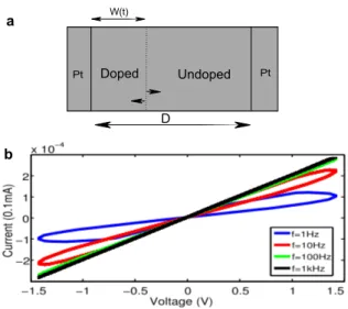
By using Verilog-A HDL, we simulate the behavior of memristor, based on its behavioral equations. To investigate the characteristics of memristor in electrical circuits, the Verilog-A model of memristor behavior must be applied as a circuit element in the HSPICE netlist. In the HSPICE circuit, we apply a sinusoidal source to observe the memristor reaction in a simple circuit consisting of the memristor and the sinusoidal source. Figure 3.b depicts i − v plot of memristor terminals that we measured in our simulation. This i − v plot, which is the most significant feature of memristor [21], is namely called “pinched hysteresis loop”. The i − v characteristic demonstrates that memristor can “remember” the last electric charge flowing through it by changing its memristance. Therefore, we can use the memristor as a latch to save the data and also as a switch for computing. Moreover, in Figure 3.b, it is depicted that the pinched hysteresis loop is shrunk by increasing frequency. In fact, when the frequency increases toward infinity, memristor behavior is similar to a linear resistor.
3
Memristor classification based on different materials and
applications
A memristor is generally made from a metal-insulator-metal (MIM) sandwich with the insulator usually consisting of a thin film like TiO2 and a metal electrode like Pt. A memristor can
be made from any Metal Insulator Metal (MIM) sandwich which exhibits a bipolar switching characteristic. It means that TiO2 and Pt are not the only materials to fit the criteria for a
Pt Pt D W(t) Doped Undoped −1.5 −1 −0.5 0 0.5 1 1.5 −2 −1 0 1 2 x 10⁻⁴ Current (0.1mA) Voltage (V) f=1Hz f=10Hz f=100Hz f=1kHz a b
Figure 3: Memristor schematic and behavior: a) the memristor structure, the difference in applied voltage changes doped and undoped regions, b) current versus voltage diagram, which demonstrates hysteresis characteristic of a memristor, in the simulation we apply the sinusoidal input wave with an amplitude of 1.5v, different frequencies, RON = 100Ω, ROF F = 15kΩ, D = 10nm, µv= 10−10cm2s−1V−1.
and ZrO2 as substitutes for TiO2, also using TiN or Ti/TiN electrode instead of Pt. Basically,
any two-terminal black box is called a memristor only if it can present a pinched hysteresis loop for all bipolar periodic input signals. Following we discuss four most significant materials for memristor fabrication namely:
• Resistive memristor • Spintronic memristor
• Organic (Polymeric) memristor • Ferroelectric memristor
3.1
Resistive Memristor
Before the memristor getting well-known, resistive materials have already been widely used in the resistive random access memories (ReRAM/RRAM) [23]. The storage function of ReRAM is realized by an intrinsic physical behavior in ReRAM, that is called resistive switching. The resistive material can be switched between a high resistance state (HRS) and a low resistance state (LRS) under an external electrical input signal. The TiO2memristor is a ReRAM fabricated
in nanometre scale (2-3 nm) thin film that is depicted in Figure 3.a , containing a doped region and an undoped region. Strukov et al. [6] exploit a very thin-film TiO2 sandwiched between
two platinum (Pt) contacts and one side of the TiO2 is doped with oxygen vacancies, which are
positively charged ions. Therefore, there is a TiO2junction where one side is doped and the other
is undoped. Such a doping process results in two different resistances: one is a high resistance (undoped) and the other is a low resistance (doped). The application of an external bias v(t) across the device will move the boundary between the two regions by causing the charged dopants to drift. How TiO2 could change and store the state has been introduced in 2.2.
The obvious disadvantage of the first published TiO2 memristor was its switching speed
(operate at only 1Hz). The switching speed was not comparable with SRAM, DRAM and even flash memory. Flash exhibit writing times of the order of a microsecond and volatile memories have writing speeds of the order of hundreds of picoseconds. Many research groups in different labs published their fabrication results to demonstrate a faster switching speed device. In October 2011, HP lab developed a memristor switch using a SET pulse with a duration of 105 ps and a
RESET pulse with a duration of 120 ps. The associated energies for ON and OFF switching were computed to be 1.9 and 5.8 pJ, respectively which are quite efficient for power-aware computations. The full-length D (Figure 3.a) of the TiO2memristor is 10 nm [24] that proposes high-density
devices in a small area in VLSI.
A research team at the University of Michigan led by Wei Lu [12] demonstrated another type of resistive memristor that can be used to build brain- like computers and known as amorphous silicon memristor. The Amorphous silicon memristor consists of a layered device structure including a co-sputtered Ag and Si active layer with a properly designed Ag/Si mixture ratio gradient that leads to the formation of a Ag-rich (high conductivity) region and a Ag-poor (low conductivity) region. This demonstration provides the direct experimental support for the recently proposed memristor-based neuromorphic systems.
Amorphous silicon memristor can be fabricated with a CMOS compatible simple fabrication process using only common materials which is a great advantage of using amorphous silicon devices. The endurance test results of two extreme cases with programming current levels 10nA and 10mA are 106 and 105 cycles respectively. We note the larger than 106 cycles of endurance
with low programming currents are already comparable to conventional flash memory devices. Wei Lu team have routinely observed switching speed faster than 5ns from the devices with a few mA on-current. The switching in this device is faster than 5 ns with a few mA on-current that make it a promising candidate for high-speed switching applications. However, before the devices can be used as a switch, they need to go through a high voltage forming process (typically ≥ 10 V) which significantly reduces the performance of power efficiency of devices [25]. Moreover, the retention time (data storage period) is still short (a few months).
3.2
Spintronic Memristor
Spintronic memristor changes its resistance by varying the direction of the spin of the electrons. Magnetic Tunneling Junction (MTJ) has been used in commercial recording heads to sense magnetic flux. It is the core device cell for spin torque magnetic random access memory and has also been proposed for logic devices. In a spintronic device, the electron spin changes the magnetization state of the device. The magnetization state of the device is thus dependent upon the cumulative effects of electron spin excitations [26]. MTJ can be switched between a LRS and an HRS using the spin-polarized current induced between two ferromagnetic layers. If the resistance of this spintronic device is determined by its magnetization state, we could have a spintronic memristor with its resistance depending upon the integral effects of its current profile.
The use of a fundamentally different degree of freedom which allows for the realization of memristive behavior is thus desirabled by Pershin and Di Ventra [9]. They demonstrated that the degree of freedom is provided by the electron spin and memristive behavior is obtained from the broad class of semiconductor spintronic devices. This class involves systems whose transport properties depend on the level of electron spin polarization in a semiconductor which is influenced by an external control parameter (such as an applied voltage). Pershin and Di Ventra considered a junction with half-metals shown in Figure 4 (ferromagnets with 100% spin-polarization at the Fermi level), because these junctions react as perfect spin-filters, therefore they are more sensitive to the level of electron spin polarization. They observed memristor behavior in the i − v curve of these systems. This means the proposed device is controllable and tunable. Furthermore, the device can be easily integrated on top of the CMOS. The integration of the spin torque memristor on CMOS is the same as the integration of magnetic random access memory cell on CMOS [27]. This has been achieved and commercialized in magnetic random access memory.
The potential applications of spintronic memristor are in multibit data storage and logic, novel sensing scheme, low power consumption computing, and information security. However, the small resistance ON/OFF ratio remains a notable concern for spintronic memristor devices.
Figure 4: Spintronic memristor:Physical schematic of the circuit made of an interface between a semiconductor and a half-metal (ferromagnets with 100% spin-polarization at the Fermi level) (From [9]).
3.3
Organic (Polymeric) Memristor
In 2005 Erokhin et al. [28] at the university of Parma reported a polymeric electrochemical element for the adaptive networks. Even though it was not called a memristor, however mainly its characteristics corresponds to the hypothetical memristor. At the heart of this device, there is a conducting channel, a thin polyaniline (PANI) layer, deposited onto an insulating support with two electrodes. A narrow stripe of solid electrolyte doped Poly Ethylene Oxide (PEO) which is formed in the central part of the channel and used for the redox reactions. The area of PANI under PEO is the active zone (see Figure 5). A thin silver wire is inserted into the solid electrolyte to provide the reference potential; such a wire is connected to one of the electrodes on the solid support, kept at the ground potential level.
Conductivity variations and memory properties of the organic memristor are due to the redox reactions occurring in the active zone, where PANI is reversibly transferred from the reduced insulating state into the oxidized conducting one [8]. In analogy with the nomenclature used in Field Effect Transistors (FETs), the two electrodes that are connected with the PANI film are called the source and drain electrodes, while the wire immersed in the PEO is called the gate electrode. In the normal operation of the device, the source and the gate electrodes are kept at ground potential, and a voltage is applied to the drain electrode. Therefore, we can consider the organic memristor as a two-terminal device. The polymeric memristor, compared to the resistive memristor, can better meet the criteria of the theoretical memristor, as its resistance is generally governed by the charge transfer.
The Polymeric memristor was investigated in pulse mode, mimicking the synaptic behavior of signal transmission in neural systems. The phenomenon that the PANI conductivity, when connected to a positive signal excitation which is gradually increased similar to the synapse behavior in real biological neural systems, described in the Hebbian rule. Simple circuit based on the polymeric memristor has already been designed to realize both supervised and unsupervised learning in neural networks [8]. Organic materials present several advantages in terms of functionality, the deposition technique, costs and above all for the relative ease with which the material properties may be tailored by a chemical approach [29]. Organic memristor operates with very low power energy. The transformation to the conducting state occurs at potentials +0.4 - +0.6 V and transformation into the insulating state take place at potentials lower than +0.1 V [30].
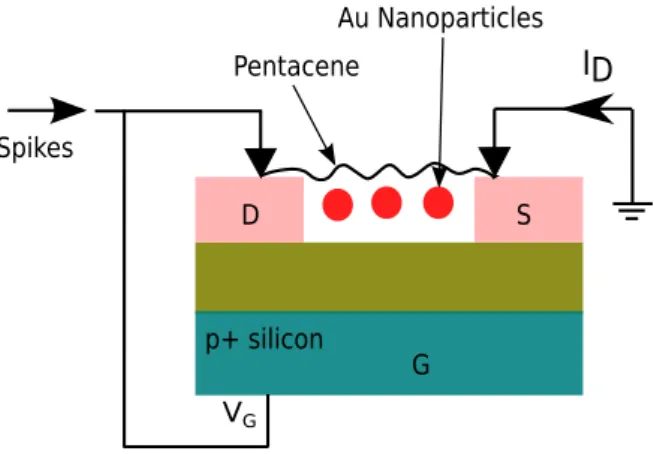
There is another type of organic memristor namely Nanoparticle Organic Memory Field Effect Transistor (NOMFET). NOMFET is made of conjugated molecules and metal nanoparticles (NPs). This device is initiated and fabricated by the institute of microelectronics and nanotechnology at Lille university [10]. NOMFET consists of a bottom-gate and source-drain contact organic transistor configuration. The gold NPs (5 nm in diameter) were immobilized into the source-drain channel by applying self-assembled monolayer covered by a thin film of Pentacene as it is shown in
Figure 5: Organic (polymeric) Memristor: the active channel is formed by PANI on top of a support and two electrodes. The region between PANI and PEO is called the ‘active zone’, and conductivity transformation is performed here.
Figure 6. The NOMFET has the capability of mimicking synaptic properties as a volatile memory. We have used NOMFET in our research to make a new type of synapse [31]. Consequently, we will discuss it more in details.
ID
VG Spikes Pentacene Au Nanoparticles p+ silicon D S GFigure 6: Physical structure of the NOMFET. It is composed of a p+ doped bottom-gate covered with silicon oxide. Source and drain electrodes are made of gold and Au NPs are deposed on the inter-electrode gap before the pentacene deposition.
3.4
Ferroelectric Memristor
Ferroelectricity is a property of certain materials which have a spontaneous electric polarization that can be reversed by the application of an external electric field. The ferroelectric memristor is based on a thin ferroelectric barrier sandwiched between two metallic electrodes. Therefore, these two opposite polarization states can be used to represent binary bits ‘0’ and ‘1’, thus resulting in the advent of the Ferroelectric Random Access Memory (FeRAM). Due to FeRAM nonvolatility, ferroelectric materials have been widely used in automobile equipment, ID/smart card, Radio Frequency Identification (RFID) and other embedded memory applications [32].
Chanthbouala, A. et al. [7], showed voltage-controlled domain configurations in ferroelectric tunnel barriers yield memristive behavior with resistance variations exceeding two orders of magnitude and a 10 ns operation speed. They reported Piezoresponse Force Microscopy (PFM) images and electrical transport measurements as a function of the amplitude, duration and the repetition number of voltage pulses in the 10-200 ns range. In tunnel junctions with a ferroelectric barrier, switching the ferroelectric polarization induces variations of the tunnel resistance, with resistance contrasts between the ON and OFF states of several orders of magnitude. The low-resistance state (RON) corresponds to the ferroelectric polarization pointing up (P ↑), and the
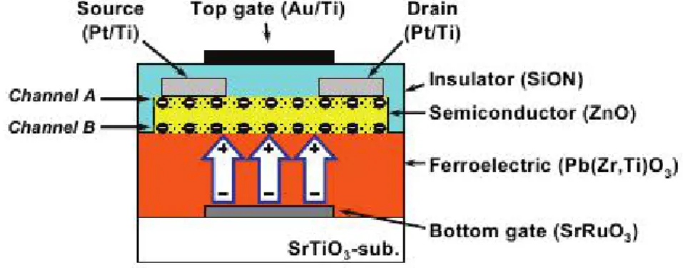
Positive and negative trains of pulses applied consecutively with +2.9 V and -2.7 V amplitude. In the analogy with the operation of FeRAM, the large ON/OFF ratio in ferroelectric tunnel junctions (FTJs) has so far been considered only for binary data storage, with the key advantage of non-destructive readout and simpler device architecture, however still non-CMOS compatible. In another study, Y.Kaneko et al. [33] presented a new transistor and implemented it by all oxide-based ferroelectric thin films, which include SrRuO3(SRO: bottom gate electrode), Pb(Zr,Ti)O3
(PZT: ferroelectric), ZnO (semiconductor), and SiON (gate insulator) Figure 7. They have demonstrated the conductivity modulation of the interface between two oxides, ZnO and PZT, in a FeFET, is applicable for a nonvolatile memory which has the same memristive operation. Ferroelectric-based memristor cell can be expected to be very suitable for the nonvolatile memory array configuration and the future neuromorphic systems embedded in the intelligent transparent electronic applications [34].
Figure 7: Ferroelectric Memristor, the OxiM transistor has dual channels at the upper and lower sides of the ZnO film, which are controlled independently by the top gate and the bottom gate, respectively. The bottom FET has the gate (SRO layer) and insulator (PZT ferroelectric layer) constituting a FeFET that has memory characteristics (from [33]).
3.5
Evaluation of Memristor with different materials
After 2008, there have been many articles related to memristors and memristive devices. Here we evaluate the four types of memristors using different materials. TiO2 memristor is the first
fabrication of memristor device which is considered as one of the most promising ones. There are hundreds of publications related to TiO2 memristor . Recently, Stanley Williams research group
enhanced the characteristics of TiO2memristor such as switching speed, programming endurance,
and retention time which made TiO2 memristor the best candidate to apply in commercial
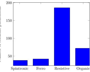
usages. Chen Yirin [26, 27] assistant professor at the University of Pittsburgh, published 49 articles in memristor technology and application are working on spintronic memristor, Pershin and Di Ventra [9] are the other researchers who trying to improve spintronic memristive devices characteristics to use it as a nonvolatile memory. Organic materials present several advantages, therefore, could be the next proper candidate to fabricate memristive devices. The last material that we have evaluated here is ferroelectric memristor. After publishing a ferroelectric memristor in Nature materials journal [7] this type of fabrication is introduced as another option for building Memristor. We sum up specifications and characteristics of these five classes of memristor material in Table 1. Lei Wang et al. [35] discussed another type of memristors such as manganite memristor and Resonant-Tunneling Diode (RTD) memristor. We note that the magnetic memristor has the similar behavior to the ferroelectric type of memristive devices. RTD has more potential to react as a complementary device beside memristor for neural network applications e.g., Cellular Neural Networks (CNN) [36]. A quantitative comparison respecting the number of published paper specifically in fabrication and material of different classes of the memristors is presented in Figure 8.
Spintronic Ferro Resistive Organic 50
100 150 200
Different types of memristor devices
Num b er of scien tific publications
Figure 8: Number of publications for each type of memristors.
4
Potential applications of memristors
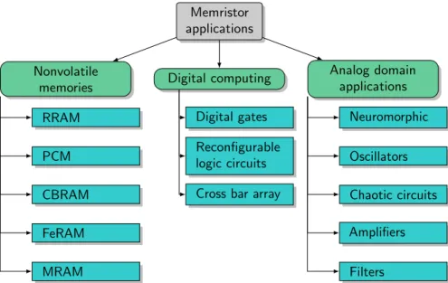
In the previous section, we have discussed the different type of memristive materials. In this section, we study the potential application of memristors. we divided the applications into three main classes: nonvolatile memories, digital computing, and analog domain applications. The classification in addition to the practical application examples is depicted in Figure 9. This classification may cover most of the recent applications, however, the memristor is a novel device which new capabilities may be introduced soon in various areas of research. Therefore, the novel applications are dramatically anticipated.
4.1
Memristor-based nonvolatile memory
Memristor-based nonvolatile memory is the most obvious application of memristors [37]. The nonvolatile, memristor-based memory cell compared to SRAM and DRAM, can exhibit non-volatility, good scalability, compatible with conventional CMOS electronics, and the last but not the least, it has no leakage power. Several types of memories are introduced using memristor nanodevice. Resistive RAM (RRAM) [38], Phase change memory (PCM) [39], Conductive Bridge memory (CBRAM) [40], ferroelectric memory (FeRAM) [7] and the spintronic memristor that can be a promising replacement for Magnetic memory (MRAM) [41]. A memory array of Memristors what is called a resistive RAM or RRAM is another form of memristor memory. RRAM operates faster than phase-change memory (PCRAM), and it has simpler and smaller cell structure than
Memristor Advantage Disadvantage Applications University-Lab Resistive small scale, fast switching,
simple structure
still non-reliable for commercial
memory, logic gates, neuromorphic, ana-log devices
HP Lab
Spintronic magnetic memory match technology
the small resistance ON/OFF ratio
Neuro-inspired sys-tems, memory
University of Pitts-burgh, US
Organic relative ease with chemical materials, work with ultra-low power
slow switching artificial synapse Parma/Lille University
Ferroelectric suitable for the nonvolatile memory array
slow switching, Non-CMOS Compatible
synapse, RRAM Panasonic, Japan & Thales, France
Table 1: Table of different class of memristors based on different materials and its applications, the first university/lab announcement of the device is listed too.
magnetic memory (MRAM).
4.2
Digital computing
Another possible application of memristor is digital design and computation. Memristors can be applied in hybrid CMOS-memristor circuits, or as a basic component to built the logic gates [42]. One remarkable logic application is using memristor as a reconfigurable switch (FPGA) [43]. The implication logic synthesis [17] and crossbar array architecture [18] are two alternatives presented a the new approaches to make efficient digital gate library. A comprehensive review and implementation of both digital computing approach is discussed in [44].
4.3
Analog domain applications
Another further research area of memristive devices is analog domain application. Simple circuits of memristors with a single capacitor or inductor are discussed in [45]. There are several research work in analog domain using memristors such as neuromorphic computing, amplifiers, memristor oscillators, filters and chaotic circuits (see e.g. [46], [47], [48], [49]).
Most interesting and recent study field in analog domain that we will focus on it more in our research is neuromorphic or neuro-inspired computation. It is believed this approach is promising for yielding innovations in future cognitive computing, hence will get probably more attention in the near future of research. The key to the high efficiency of biological neural systems is the large connectivity between neurons that offers highly parallel processing power. Another key factor of high efficiency of biological neural network is the connection plasticity. The synaptic weight between two neurons can be precisely adjusted by the ionic flow through them and it is widely believed that the adaptation of synaptic weights enables the biological neural systems to learn. Memristors function similarly to the biological synapses. This characteristic makes Memristors proper building blocks in neuromorphic systems, where neurons and synapses are modeled as electronic devices [12]. Memristors can be made extremely small, therefore, by applying them, mimicking the functions of a brain would be possible in near future [20]. The brain-like computing capability of the memristor-based complex spike timing- dependent plasticity (STDP) learning networks is demonstrated by Afifi et al [50]. Memristor could be applied in more efficient learning platform such as Deep Belief Networks for online learning [51, 52]. The model of memristor is used in neuromorphic hardware simulation e.g., Xnet [53] and N2S3 [54].
5
Streams of research
The ability to indefinitely store resistance values means that a memristor can be used as a nonvolatile memory. There are yet more potential applications that we did not mention previously , we point to the capacity of memristive networks in realizing demanding image processing and more specifically edge detection and face/object recognition [55]. Pershin and Di Ventra address the capability of memristors to perform quantum computation in addition to conventional neuromorphic and digital data processing [56]. Performing arithmetic operations in memristor-based structures is possible in both analog and digital approaches [57]. Another system level application is memristive Neuro-Fuzzy System [58]. However, the memristor potential goes far beyond instant-on computers to embrace one of the biggest technology challenges: mimicking the functionality of the brain. Within a decade, memristors could let us emulate, instead of merely simulate, networks of neurons and synapses. By replacing several specific transistors with a crossbar of memristors, circuit could be shrunk by nearly a factor of 10 in area and improved in terms of its speed relative to power consumption performance [20]. Computing with memristor is another interesting approach which memristor plays a crossbar switch role in the circuit. Using memristor-based circuit for performing arithmetic operations, signal processing application, dynamic load, oscillators, amplifiers, sensing application, artificial biological system, image encryption, and many other approaches are several applications of memristor that recently appeared in different research publications. In this context, we made a simple classification of
a stream of research as shown in Figure 10 that could be useful for those who want to use this flexible device in their research studies. The hybrid approaches are not in the chart, here we mention that any sort of utilization can be implemented in hybrid circuit instead of using pure memristive circuit.
6
Conclusions and summary
In this study, we have done a feasibility study on memristive nanodevice from theoretical model to practical applications. we studied the cons and pros of using different memristor devices based on the applied material to manufacture the device. As each material or type of memristor has its own characteristics, consequently one can analyze and discover the different potential of application of each type of these memristive devices more conveniently. The better understanding of physics of different memristive materials leads to discover more sophisticated applications of these devices. Four general memristive devices are surveyed namely: Resistive, Spintronic, Organic (polymeric) and Ferroelectric memristive devices. The potential application as well as advantages versus disadvantages of using each one are presented too. The resistive memristor has been applied more than others in different research works from memory to artificial synapse. The Spintronic and Ferroelectric devices show promising properties to make new nonvolatile memories. The organic memristor is more appropriate to make artificial synapse in Spiking Neural Networks. The mix combination of those materials not only propose new research studies but also take the advantages of using more useful properties of each device.
The practical applications of memristive devices are presented subsequently. Three main domains of potential applications have been classified: a)nonvoaltile memory such as RRAM, PCM, CBRAM, FeRAM and MRAM; b)digital computing domain such as logic implication and crossbar array; c)analog domain of application such as neuro-inspired computing in spiking neural networks, oscillators, filters and amplifiers. Among these applications, we focus on computation approaches by using two digital and neuromorphic domains.
Memristor applications
Nonvolatile
memories Digital computing
Analog domain applications RRAM PCM CBRAM FeRAM MRAM Digital gates Reconfigurable logic circuits Cross bar array
Neuromorphic
Oscillators
Chaotic circuits
Amplifiers
Filters Figure 9: Different memristor applications in different domains.
Bibliography
[1] Hai (Helen) Li and Miao Hu. Compact model of memristors and its application in computing systems. pages 673–678, March 2010.
[2] Yenpo Ho, Garng M. Huang, and Peng Li. Nonvolatile memristor memory: device character-istics and design implications. pages 485–490, 2009.
[3] Massimiliano Di Ventra and Yuriy V. Pershin. Memcomputing: a computing paradigm to store and process information on the same physical platform. CoRR, abs/1211.4487, 2012. [4] Sung Hyun Jo, Ting Chang, Idongesit Ebong, Bhavitavya B. Bhadviya, Pinaki Mazumder,
and Wei Lu. Nanoscale Memristor Device as Synapse in Neuromorphic Systems. Nano Letters, 10(4):1297–1301, April 2010.
[5] L. Chua. Memristor-The missing circuit element. IEEE Transactions on Circuit Theory, 18(5):507–519, September 1971.
[6] Dmitri B. Strukov, Gregory S. Snider, Duncan R. Stewart, and R. Stanley Williams. The missing memristor found. Nature, 453(7191):80–83, May 2008.
[7] Andr´e Chanthbouala, Vincent Garcia, Ryan O. Cherifi, Karim Bouzehouane, St´ephane Fusil, Xavier Moya, St´ephane Xavier, Hiroyuki Yamada, Cyrile Deranlot, Neil D. Mathur, Manuel Bibes, Agn`es Barth´el´emy, and Julie Grollier. A ferroelectric memristor, June 2012.
[8] T. Berzina, S. Erokhina, P. Camorani, O. Konovalov, V. Erokhin, and M.P. Fontana. Electrochemical control of the conductivity in an organic memristor: A time-resolved x-ray fluorescence study of ionic drift as a function of the applied voltage. ACS Applied Materials and Interfaces, 1(10):2115–2118, 2009.
[9] Yurij V. Pershin and Massimiliano D. Ventra. Spin Memristive systems. Physical Review B., 78:113309, 2008.
[10] Fabien Alibart, Stphane Pleutin, David Gurin, Christophe Novembre, Stphane Lenfant, Kamal Lmimouni, Christian Gamrat, and Dominique Vuillaume. An Organic Nanoparti-cle Transistor Behaving as a Biological Spiking Synapse. Advanced Functional Materials, 20(2):330–337, January 2010.
[11] Z. Biolek, D. Biolek, and V. Biolkov. Spice model of memristor with nonlinear dopant drift. Radioengineering, 18(2):210–214, 2009.
[12] Sung H. Jo, Ting Chang, Idongesit Ebong, Bhavitavya B. Bhadviya, Pinaki Mazumder, and Wei Lu. Nanoscale Memristor Device as Synapse in Neuromorphic Systems. Nano Lett., 10(4):1297–1301, March 2010.
[13] H. Yan, H.S. Choe, S. Nam, Y. Hu, S. Das, J.F. Klemic, J.C. Ellenbogen, and C.M. Lieber. Programmable nanowire circuits for nanoprocessors. Nature, 470(7333):240–244, 2011. [14] Garrett S. Rose. Overview: Memristive devices, circuits and systems. In ISCAS, pages
[15] Julien Borghetti, Zhiyong Li, Joseph Straznicky, Xuema Li, Douglas A. A. Ohlberg, Wei Wu, Duncan R. Stewart, and R. Stanley Williams. A hybrid nanomemristor/transistor logic circuit capable of self-programming. Proceedings of the National Academy of Sciences, 106(6):1699–1703, 2009.
[16] Garrett S. Rose, Jeyavijayan Rajendran, Harika Manem, Ramesh Karri, and Robinson E. Pino. Leveraging memristive systems in the construction of digital logic circuits. Proceedings of the IEEE, 100(6):2033–2049, 2012.
[17] E. Lehtonen, J. Poikonen, and M. Laiho. Implication logic synthesis methods for memristors. pages 2441–2444, May 2012.
[18] I. Vourkas and G.C. Sirakoulis. A novel design and modeling paradigm for memristor-based crossbar circuits. Nanotechnology, IEEE Transactions on, 11(6):1151–1159, 2012.
[19] Giacomo Indiveri, Bernabe Linares-Barranco, Robert Legenstein, George Deligeorgis, and Themistoklis Prodromakis. Integration of nanoscale memristor synapses in neuromorphic computing architectures. Nanotechnology, 24(38):384010, September 2013. arXiv: 1302.7007. [20] R. Williams. How we found the missing memristor. IEEE Spectr., 45(12):28–35, December
2008.
[21] L.O. Chua and Sung Mo Kang. Memristive devices and systems. Proceedings of the IEEE, 64(2):209–223, Feb. 1976.
[22] Wan Gee Kim, Min Gyu Sung, Sook Joo Kim, Jong Hee Yoo, Te One Youn, Jang Won Oh, Jung Nam Kim, Byung Gu Gyun, Taeh Wan Kim, Chi Ho Kim, Jun Young Byun, Won Kim, Moon Sig Joo, Jae Sung Roh, and Sung Ki Park. Dependence of the switching characteristics of resistance random access memory on the type of transition metal oxide; tio2, zro2, and hfo2. Journal of The Electrochemical Society, 158(4):H417–H422, 2011.
[23] Rainer Waser, Regina Dittmann, Georgi Staikov, and Kristof Szot. Redox-Based Resistive Switching Memories-Nanoionic Mechanisms, Prospects, and Challenges. Advanced Materials, 21(25-26):2632–2663, July 2009.
[24] A.C. Torrezan, J.P. Strachan, G. Medeiros-Ribeiro, and R.S. Williams. Sub-nanosecond switching of a tantalum oxide memristor. Nanotechnology, 22(48):485203, 2011.
[25] S.H. Jo, K.-H. Kim, T. Chang, S. Gaba, and W. Lu. Si memristive devices applied to memory and neuromorphic circuits. pages 13–16, 2010.
[26] Xiaobin Wang, Yiran Chen, Haiwen Xi, Hai Li, and D. Dimitrov. Spintronic Memris-tor Through Spin-Torque-Induced Magnetization Motion. Electron Device Letters, IEEE, 30(3):294–297, March 2009.
[27] Xiaobin Wang and Yiran Chen. Spintronic memristor devices and application. In Proceedings of the Conference on Design, Automation and Test in Europe, DATE ’10, pages 667–672, 3001 Leuven, Belgium, Belgium, 2010. European Design and Automation Association. [28] Victor Erokhin, Tatiana Berzina, and Marco P. Fontana. Hybrid electronic device based on
polyaniline-polyethyleneoxide junction. Journal of Applied Physics, 97(6):064501, 2005. [29] F. Pincella, P. Camorani, and V. Erokhin. Electrical properties of an organic memristive
system. Applied Physics A: Materials Science & Processing, 104:1039–1046, September 2011. [30] Victor Erokhin and Marco P. Fontana. Organic memristive device and its application for
[31] Mahyar Shahsavari, Pierre Falez, and Pierre Boulet. Combining a Volatile and Nonvolatile Memristor in Artificial Synapse to Improve Learning in Spiking Neural Networks. In 12th ACM/IEEE International Symposium on Nanoscale Architectures (Nanoarch 2016), Beijing, China, July 2016.
[32] L. Wang and S. Gai. The next generation mass storage devices - Physical principles and current status. Contemporary Physics, 55(2):75–93, April 2014.
[33] Y. Kaneko, H. Tanaka, M. Ueda, Y. Kato, and E. Fujii. A novel ferroelectric memristor enabling nand-type analog memory characteristics. In Device Research Conference (DRC), 2010, pages 257 –258, june 2010.
[34] S.-M. Yoon, S. Yang, S.-W. Jung, C.-W. Byun, M.-K. Ryu, W.-S. Cheong, B.H. Kim, H.C. Oh, S.-H.K. Park, C.-S. Hwang, S.-Y. Kang, H.-J. Ryu, and B.-G. Yu. Polymeric ferroelectric and oxide semiconductor-based fully transparent memristor cell. Applied Physics A: Materials Science and Processing, 102(4):983–990, 2011.
[35] Lei Wang, CiHui Yang, Jing Wen, Shan Gai, and YuanXiu Peng. Overview of emerging memristor families from resistive memristor to spintronic memristor. Journal of Materials Science: Materials in Electronics, 26(7):4618–4628, March 2015.
[36] Xiaofang Hu, Gang Feng, Shukai Duan, and Lu Liu. Multilayer RTD-memristor-based cellular neural networks for color image processing. Neurocomputing, 162:150–162, August 2015.
[37] S. Hamdioui, L. Xie, H.A. Du Nguyen, M. Taouil, and K.L.M. Bertels. Memristor based computation-in-memory architecture for data-intensive applications. In Proc. 18th Design, Automation & Test in Europe conference, Grenoble, France, March 2015.
[38] Cong Xu, Xiangyu Dong, Norman P. Jouppi, and Yuan Xie. Design implications of memristor-based rram cross-point structures. In DATE, pages 734–739. IEEE, 2011.
[39] T. Driscoll, H.-T. Kim, B.-G. Chae, M. Di Ventra, and D. N. Basov. Phase-transition driven memristive system. Applied Physics Letters, 95(4):043503, July 2009.
[40] Qi Liu, Shibing Long, Hangbing Lv, Wei Wang, Jiebin Niu, Zongliang Huo, Junning Chen, and Ming Liu. Controllable Growth of Nanoscale Conductive Filaments in Solid-Electrolyte-Based ReRAM by Using a Metal Nanocrystal Covered Bottom Electrode. ACS Nano, 4(10):6162–6168, October 2010.
[41] Hai Li and Yiran Chen. An overview of non-volatile memory technology and the implication for tools and architectures. In DATE, pages 731–736, 2009.
[42] Qiangfei Xia, Warren Robinett, Micheal W. Cumbie, Neel Banarjee, Thomas J. Cardinali, Joshua J. Yang, Wei Wu, Xuema Li, William M. Tong, Dmitri B. Strukov, Gregosry S. Snider, Gilberto Medeiros=Ribeiro, and R. Stanley Williams. Memristor-CMOS Hybrid Integrated circuits for reconfigurable logic. Nanoletters, 2009.
[43] Jason Cong and Bingjun Xiao. mrfpga: A novel fpga architecture with memristor-based re-configuration. In Proceedings of the 2011 IEEE/ACM International Symposium on Nanoscale Architectures, NANOARCH ’11, pages 1–8, Washington, DC, USA, 2011. IEEE Computer Society.
[44] Mahyar Shahsavari, M. Faisal Nadeem, S. Arash Ostadzadeh, Philippe Devienne, and Pierre Boulet. Unconventional digital computing approach: memristive nanodevice platform. physica status solidi (c), 12(1-2):222–228, January 2015.
[45] Yogesh N. Joglekar and Stephen J. Wolf. The elusive memristor: properties of basic electrical circuits.
[46] T.A. Wey and W.D. Jemison. Variable gain amplifier circuit using titanium dioxide memris-tors. IET Circuits, Devices and Systems, 5(1):59–65, 2011.
[47] M. Itoh and L.O. Chua. Memristor oscillators. International Journal of Bifurcation and Chaos, 18(11):3183–3206, 2008.
[48] S. Shin, K. Kim, and S.-M. Kang. Memristor applications for programmable analog ics. IEEE Transactions on Nanotechnology, 10(2):266–274, 2011.
[49] B. Muthuswamy. Implementing memristor based chaotic circuits. International Journal of Bifurcation and Chaos, 20(5):1335–1350, 2010.
[50] A. Afifi, A. Ayatollahi, and F. Raissi. Implementation of biologically plausible spiking neural network models on the memristor crossbar-based cmos/nano circuits. pages 563–566, 2009. [51] Emre Neftci, Srinjoy Das, Bruno Pedroni, Kenneth Kreutz-Delgado, and Gert Cauwenberghs. Event-driven contrastive divergence for spiking neuromorphic systems. Neuromorphic Engi-neering, 7:272, 2014.
[52] M. Fatahi, M. Ahmadi, A. Ahmadi, M. Shahsavari, and P. Devienne. Towards an spiking deep belief network for face recognition application. In 2016 6th International Conference on Computer and Knowledge Engineering (ICCKE), pages 153–158, October 2016.
[53] O. Bichler, D. Roclin, C. Gamrat, and D. Querlioz. Design exploration methodology for memristor-based spiking neuromorphic architectures with the Xnet event-driven simulator. In 2013 IEEE/ACM International Symposium on Nanoscale Architectures (NANOARCH), pages 7–12, July 2013.
[54] Mahyar Shahsavari, Philippe Devienne, and Pierre Boulet. N2s3, a Simulator for the Architecture Exploration of Neuromorphic Accelerators. In 2nd International Workshop on Neuromorphic and Brain-Based Computing Systems (NeuComp 2015) in DATE Conference, Grenoble, France, 2015.
[55] X. Hu, S. Duan, L. Wang, and X. Liao. Memristive crossbar array with applications in image processing. Science China Information Sciences, 55(2):461–472, 2012.
[56] Y.V. Pershin and M. Di Ventra. Neuromorphic, digital, and quantum computation with memory circuit elements. Proceedings of the IEEE, 100(6):2071 –2080, june 2012.
[57] Farnood Merrikh-Bayat and Saeed Bagheri Shouraki. Memristor-based circuits for performing basic arithmetic operations. Procedia CS, 3:128–132, 2011.
[58] F. Merrikh-Bayat and S. Bagheri Shouraki. Memristive neuro-fuzzy system. IEEE Transac-tions on Systems, Man, and Cybernetics, Part B: Cybernetics, 2012.
![Figure 1: Relations between the passive devices and the anticipating the place of the fourth fundamental element based on the relations between charge (q) and flux (ϕ) (from [6]).](https://thumb-eu.123doks.com/thumbv2/123doknet/12763495.359818/6.892.304.582.86.372/figure-relations-passive-devices-anticipating-fundamental-element-relations.webp)

![Figure 4: Spintronic memristor:Physical schematic of the circuit made of an interface between a semiconductor and a half-metal (ferromagnets with 100% spin-polarization at the Fermi level) (From [9]).](https://thumb-eu.123doks.com/thumbv2/123doknet/12763495.359818/11.892.320.576.102.262/spintronic-memristor-physical-schematic-interface-semiconductor-ferromagnets-polarization.webp)