Deeply Scaled CMOS for RF Power Applications
by
J*rg Scholvin
B.S., Massachusetts Institute of Technology (2001)
M.Eng., Massachusetts Institute of Technology (2001)
Submitted to the Department of
Electrical Engineering and Computer Science
in Partial Fulfillment
of the Requirements for the Degree of
Doctor of Philosophy
at the
MASSACHUSETTS INSTITUTE OF TECHNOLOGY
June 2006
© 2006 Massachusetts Institute of Technology. All rights reserved.
0
Department of Electrical Engineering and Computer Science May 23 2006Certified by
Jesuis A. del Alamo
.. ..
essor of Electrical Engineering Thesis Supervisor
Certified by
Arthur C. Smith Chairman, Department Committee on Graduate Thesis
ARCHIVES
MASSACHUISETS INSTITUTE OF TECHNOLOGYNOV 0,2 2006
LIBRARIES
Author1% I
s
Deeply Scaled CMOS for RF Power Applications
by
J6rg Scholvin
Submitted to the Department of Electrical Engineering and Computer Science in Partial
Fulfillment of the Requirements for the Degree of Doctor of Philosophy in Electrical
Engineering
Abstract
The microelectronics industry is striving to reduce the cost, complexity, and form factor of wireless systems through single-chip integration of analog, RF and digital functions. Driven by the requirements of the digital system components, the 90 nm and 65 nm technology nodes are currently emerging as platforms for highly integrated systems. Achieving such integration while minimizing the cost of adding specialized RF modules places high demands on the base CMOS technology. In this regard, the integration of the power amplifier (PA) function becomes an increasing challenge as technology geometries and supply voltages scale down. Gate length (Lg) scaling yields improved frequency response, promising higher power-added efficiency (PAE), a key RF PA consideration. This benefit comes at the cost of a lower drain voltage, which demands a higher output current and thus wider devices in order to produce a given output power level (Po,,).
In this work, we have investigated the potential of deeply scaled CMOS for RF power applications, from 0.25 um down to 65 nm. We demonstrate the frequency and power limitations that the different CMOS technologies face, and describe the physical mechanisms that give rise to these limitations. We find that layout considerations, such as splitting a single large device into many smaller parallel devices, become increasingly important as the technology scales down the roadmap, both for power and frequency. We also show that parasitic resistances associated with the back-end wiring are responsible for placing an upper limit on the RF power that can be obtained for a single bond pad.
We demonstrate a power density of 31 mW/mm for the 65 nm node, with PAE in excess of 60% at 4 GHz and 1 V. Similar results are obtained in 90 nm, where a peak PAE of 66% was measured at 2.2 GHz and 1 V, with a power density of 24 mW/mm.
We find that efficient integrated PA functionality for many applications can be achieved even in a deeply-scaled logic CMOS technology. For low power levels (below 50 mW), we find that the 65 nm CMOS devices offer excellent efficiency (>50%) over a broad frequency range (2-8 GHz). Their RF power performance approaches that of 90 nm devices both in peak PAE and output power density. This is possible without costly PA-specific add-ons, or the use of higher voltage input-output (I/O) device options. However, since I/O devices are often included as part of the process, they represent a real option for PA integration because they allow for higher power densities. The 0.25 /im I/O device that is available in the 90 nm process, when biased at Vdd = 2.5 V showed excellent results, with
a peak PAE of 60% and an output power of 75 mW (125 mW/mm) at 8 GHz.
Thesis Supervisor: Jesuis A. del Alamo Title: Professor
Acknowledgements
The past several years working on this thesis have been an amazing experience of learning
and
working with extraordinary people. I would like to thank my thesis advisor,
Prof. Jesus del
Alamo, for giving me the privilege to work in his group and to learn from him
the skills and
knowledge I have acquired in the past years. Being able to learn from a great teacher
has been an
invaluable resource.
I would also like to thank my thesis readers, Prof. Joel Dawson and Prof. Charles
Sodini for
providing valuable guidance that helped me to improve the work presented
in this thesis. I
deeply appreciate the feedback and suggestions that I have received.
This work would not have been possible without the generous support of IBM, through
the PhD
fellowship program and faculty awards. I would like to thank my mentor at IBM
and former del
Alamo student, David Greenberg, for making this collaboration possible through
his tireless
efforts and help. I also want to thank David Harame, Scott Parker, Greg Freeman
and Jack
Pekarik for their enthusiastic support of the project. I have spent three summers working
at IBM
Burlington VT, and Fiskill NY, on projects directly related to this thesis. Among the many
great
people I have met at IBM, I would like to thank Susan Sweeney and Jae Rascoe
for their device
measurement expertise, and Ramana Malladi for many interesting conversations about
my work.
I want to thank everyone in the del Alamo research group for their support, inputs and outputs:
former students Jim Fiorenza and Samuel Mertens, Niamh Waldron, Joyce Wu,
Anita
Villanueva, Melinda Wong, Jungwoo Joh, and post-doc's Tetsuya Suemitsu and Dae-Hyun
Kim,
as well as visiting scientist Joerg Appenzeller. They helped to make the office-
and lab-life
enjoyable.
I would like to thank my wife Sylvie for being there for me and understanding the sometimes
erratic work-schedule of a graduate student.
And sometimes, great wisdom can be found in the most unexpected places:
Contents
1. Introduction
1.1. Literature Background: State of the Art
1.2. Application Space for RF Power CMOS
1.3. Thesis Goals
1.4. Outline
2. Experimental
2.1. Technology Description
2.2. Device Layout
2.3. DC and S-Parameter Characterization
2.4. Power Characterization
3. 90 nm Technology
3.1. Results
3.1.1. RF Power Performance of the 90 nm Logic Device
3.1.2. RF Power Performance of Other Device Options
3.2. Discussion
3.3. Conclusion
4. 65 nm Technology
4.1. Experiments
4.2. Discussion
4.3. Technology Scaling: 65, 90 and 250 nm
5. First Order RF Power Model
5.1. Model Structure
5.2. Parameter Extraction
5.3. Model Results
6. Discussion
6.1. Frequency and Power Limits of
65 nm, 90 nm and 250 nm technologies
7. Conclusions
Appendix
A Power Measurement Theory
B Load-pull Setup
C Device Library
Bibliography
89
101
105
117
List of Figures
1.1 Number of power-amplifier research results published in IEEE journals and conferences in 1993 (top) and
2003 (bottom), by material and device types. In 2003, 16% of the overall activity was taking place in CMOS technology.
17
1.2 Research activity as a function of time by material (left) and within silicon (right) by device type.
18
1.3 Power density as a function of bias voltage. Boundaries of different materials and device types are shown.
CMOS is able to operate at voltages below 5 V, and demonstrates power densities comparable to the other materials.
19
1.4 Physical gate length of CMOS power devices and amplifiers, as a function of time, for IEEE published
research. The trend towards scaling the gate exists even in RF power CMOS, as the data suggests. The CMOS technology nodes are marked by the arrows. Shorter gates generally result in higher gain (through
transconductance) and therefore better efficiency and performance - though at the cost of reduced bias
voltage and output power (see Figs. 1.3, 1.5).
19
1.5 Physical gate length as a function of operation frequency for CMOS RF power devices and amplifiers. Device
operation at higher frequencies requires a shorter gate, as can be seen from the data.
20
1.6 Impact of gate length scaling on power added efficiency for class A to B devices, in a selected frequency
band. Efficiency improves with shorter gates, due to higher transconductance and improved gain and frequency response. Data includes MESFET and HEMT type devices.
20
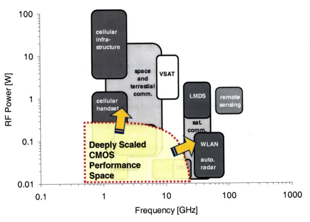
1.7 Overview of the different applications that require RF power. The sketch shows the broad range of
frequencies and power levels that are required in different applications.
22
1.8 Technology landscape in the frequency-power space. Silicon based technologies occupy the low frequency regions, while compound semiconductors are used for higher frequencies and power levels.
22
1.9 Illustration of how RF CMOS devices exhibit limitations of power and frequency. The goal of this thesis is to
identify these limits, and study how they can be pushed out.
26
2.1 Vertical drain layout (source = red, drain = blue, gate=green). The structure is symmetric, and only half is
shown. The symmetry plane is indicated. The layout design is patent pending.
29
2.2 DC sweep for the standard 90 nm device (1x48x16 pm), with Vgs from 0.4V to 1V in 0.1V steps.
30
2.3 S-parameters (0.5-50 GHz) for the standard 90 nm device (1x48x16 pm), biased at Vds=1V, Vgs=0.58V. S11
and S22 are plotted on the left, and S21 and 50 times S12 are plotted on the right.
31
2.4 A typical power sweep, showing the power added efficiency (PAE) and the transducer gain, as a function of
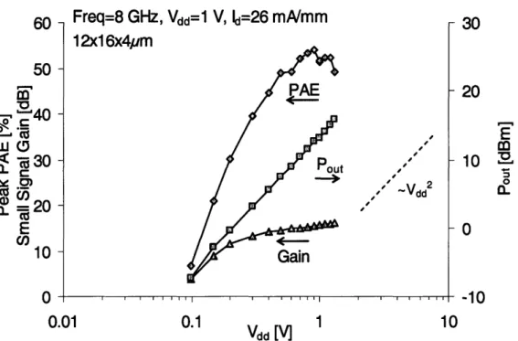
the measured output power. This measurement shows the 65 nm standard device (768 Am width), at 4 GHz in class AB bias.
33
3.1 Power performance at 2.2 GHz of a thin-oxide 90 nm device (1x48x16 Am) and a device array (8x48x16 Am),
both biased at Vdd = 1 V and Id = 26 mA/mm. Impedances were optimized for the best linearity-efficiency tradeoff.
3.2 Peak PAE and output power at peak PAE as a function of
frequency
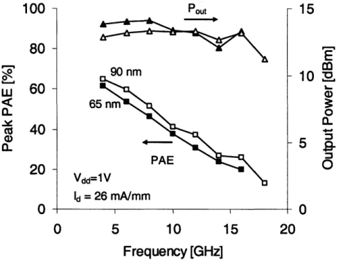
for the standard 90 nm device (1x48x16Alm). All measurement points were taken at Vdd = I V, Id = 26 mA/mm, and impedances were reoptimized at
each frequency. The output power is roughly independent of frequency, while the peak PAE is dropping as the frequency increases.
38
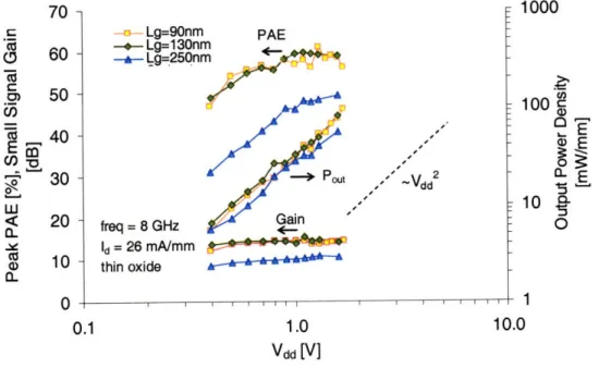
3.3 Gain, PAE and output power density at peak PAE point as a function of Vdd for thin oxide devices of three
different gate lengths at 8 GHz. Impedances and input power drive were re-optimized at each Vddfor each device.
40
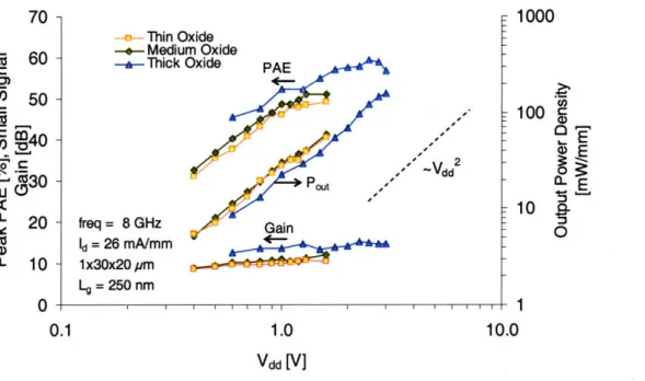
3.4 Gain, PAE and output power density at peak PAE as a function of Vddfor 250 nm devices with three different
gate oxide thicknesses at 8 GHz. Impedances and input power drive were re-optimized at each Vddfor each device.
41
3.5 Gain, PAE and output power density at peak PAE point as a function of Vdd when scaling both L, and gate
oxide thickness at 8 GHz. Impedances and input power drive were re-optimized at each Vddfor each device.
42
3.6 Comparison of the 90 nm thin and 250 nm thick oxide devices. Both devices can achieve similar peak PAE
levels, though at different operating voltages and power densities, as indicated.
42
3.7 Comparison of f,, for the devices in Table I operating at Vnomina. Small width devices (right axis) with their
pad parasitics de-embedded offer a peak
f,
of 100 to 200 GHz. Thef,.
of the power devices (left axis) usedin this paper are not de-embedded, and show a much lower f,, due to the class AB bias (Id = 26 mA/mm) and
the parasitics associated with the pads, the large number offingers and their width (e.g. R, and Cgd).
43
3.8 Load-line comparison for the 90 nm thin and 250 nm thick oxide devices. Measured DC I-V characteristics of
the two devices are shown, with the approximate Vd,,sa indicated. The 90 nm device's Vds,sat is lower than that of the 250 nm device. Load-lines, based on the impedances used in the power measurements of Fig. 3.5, are
also shown at Vdd = 1V and 2.5V.
45
4.1 Power characteristics of two 65 nm devices with a total gate width of 768 lm at 4 GHz. The 12 cell device
delivers a peak PAE of 65.7% at a power of 13.8 dBm (31.2 mW/mm) at a voltage of 1 V.
50
4.2 Power performance for the 12x16x4 Alm, 65 nm device at 8 GHz vs. Vd. For each Vdd the device is tuned to
peak PAE. The gain is the small signal gain.
51
4.3 Output characteristics of the 12x16x4
pm,
65 nm device for V, = 0.2 to 1 V in 0.2 V steps. For small valuesof Vgs and high values of Vds, impact ionization effect can be seen. Overlapping the device characteristics is the load line corresponding to a bias point of I V.
52
4.4 Performance of a 65 nm device (12x16x4 tm) as a function of bias current. Idq is the quiescent drain current
(no Pin), and Id is the drain current at peak PAE. The device is self biasing and the peak PAE, Pout and Gain do not change much with bias current.
52
4.5 Power performance as a function of device size for 65 nm devices (1, 2, 3, 4 and 6 parallel cells of 64x12 Alm
each) and 90 nm devices (1, 2, 4 and 8 cells of 48x16 Atm). As the number of cells and thus device width increases for the 65 nm devices, PAE drops while Pout saturates. The behavior of 90 nm is very different as Pout continues to increase with device size. Given the independence of power on frequency over the range that is studied in this work (see Fig. 4.13), we have included a data point for a very wide 90 nm device (6.1 mm) that was measured at 2.2 GHz.
4.6 (a, left) Simplified model schematic to create a multi-cell device from a number of single cell devices (b, right). The intrinsic device cells of the single cell and the multi-cell device are identical. Adding parallel single cell devices requires parasitic resistances to match the increased wire resistance of the multi-cell device's backend. The model parameters were extracted using S-parameter measurements from a single cell and the multi-cell device.
54
4.7 Y11 comparison of a two-cell device (2x48x16 Am) with the model. When using two parallel 1x48x16 Am
device measurements, the match with the two-cell device is mediocre. Adding parasitic resistances on the source, gate and drain, as shown in Fig. 4.6b, results in a much better match with the two-cell measurements. The other Y-parameters exhibit a similar picture and are omitted to preserve clarity in the graph.
54
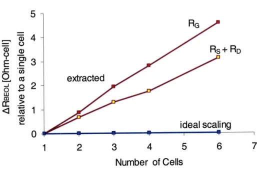
4.8 Small signal extracted parasitic scaling resistances (R, and Rs+Rd). To construct a multi-cell device from
single-cell devices, these resistance must be added into the single cell unit (NFx WF = 48x12 ALm = 768 jm) as shown in Fig. 4.6b.
56
4.9 Model of the peak PAE (left) and Pou, performance (right) with scaling, matched to the 768 jm device, and
using the resistances from Fig. 4.8. The graph also shows the ideal scaling behavior, as well as that of reducing the extracted resistance by 50%.
57
4.10 Correlation of peak PAE with fm,, (extracted at Vgs = 0.4 V and Vds= V) for the 5 different 65 nm device
sizes (each cell is a 65 nm device of 64x12 im), as well as the optimized device layout (12 cells 16x4 jlm
devices)
60
4.11 f,,, vs. unit finger width for a 1 cell device, keeping overall width the same (NF x WG,F = 768 jm). Large finger width hurts fm,a because of R,. Narrow finger width hurts because of distributed effects involving the
large number of device fingers that must be parallelized.
60
4.12 Breaking the 65 nm device up into multiple cells in parallel, both the number of fingers and their unit width
are scaled down at the same time. This method can achieve higher f,,, values (51.4 GHz vs. 43.7 GHz) at
identical bias conditions. However, too many cells in parallel hurt performance due to the excessive wiring required, as seen by the drop in fm,x as the number of cells increases beyond 50.
61
4.13 Performance comparison of the 90 nm and 65 nm devices as a function of frequency. Both devices have a total width of :768 Am (65 nm: 64x12 Am and 90 nm: 48x16 jLm). The output power is independent of frequency, and essentially identical for both devices, while the peak PAE for this 65 nm device is slightly
lower.
62
4.14 Peak PAE and output power density at 8 GHz as a function of Vddfor three different CMOS technologies
64 5.1 DC characteristics of the 90-nm device (1x48x16 Am) with indicated load-lines. The model must focus on the
device regions that the load-line occupies. The DC data shows self heating effects for high Vds, Id values.
68
5.2 Full device model (top) and simplified equivalent model (bottom). The R-C networks on the drain and gate
are simplified into a single frequency dependent resistor. The assumption is that the reactive components of the device are resonated out by the source and load impedances. The other model elements include the current generator (k, VT, exp), the breakdown voltage (BV) and the on-resistance (Ron).
69
5.3 Example fit of the subthreshold curve at Vds= Il V, for the 90 nm device. The extracted values for VT, k and exp
are shown in Table 5.1.
5.4 Measured output resistance (Real(Y22)) as a function of Vgs, for two frequencies at Vd= I V. The data shows
that Ro is bias dependent. The model assumes a bias-independent Rdo• Choosing a constant value around threshold (indicated) provides the best compromise.
72
5.5 Measured input resistance (Real(Y11)) as a function of Vg, for two frequencies at Vds= 1 V. The data shows
that Rgs is largely bias independent. Model parameters were chosen at V,= VT.
72
5.6 Model performance comparison with measured power performance, as a function offrequency. The model
uses the parameters of Table 5.1. The model for each technology roughly matches the behavior of the data. The output power is frequency independent up to very high frequencies, while the peak PAE decreases.
74
5.7 Model performance compared to the 65 nm device scaling measurements. Depending on the parasitic
resistance for the overall device, the drop in peak PAE and the maximum output power can vary significantly.
The model assumes a constant backend resistance that does not scale with the number of cells.
74
6.1 Constant PAE contours illustrating the output power that can be achieved at a given frequency. The higher
the desired PAE, the lower the power and frequency. The power has an upper limit set by the backend parasitics, while the frequency has an upper limit related to the device gain andf,,• The values in the graph are based on the 90 nm technology, which we expect to be able of delivering 140 mW of power (Pat,) with a
maximum power at Nc.sa,= 12, and a maximum operating
frequency of 21 GHz (fa).
80
6.2 Impact of device layout on the device fn,,. The standard single cell device is shown in the solid bars. Using
an optimized device layout by breaking the device up into multiple smaller cells, f,,a can be improved significantly. This becomes more critical as the technology is scaled down.
82
6.3 Estimated contour of 50% peak PAE, for three different technologies, illustrating the power vs. frequency
behavior. The estimates are based on extrapolation of measured data. The limited power of the 65 nm device in chapter 4 can be expected to improve with a different layout design (shown as dotted lines).
82
6.4 Estimated 50% peak PAE contours, from Fig. 6.2, redrawn taking the device layout optimization into
account. Layout optimization can help to push out the frequency limit for the PA device. The 65 nm technology profits from optimized layout the most, as seen in Fig. 6.3.
84
7.1 Expected 50% peak PAE contours, from Fig. 6.4. This figure assumes an optimized backend layout for
the 65 nm devices, resulting in an improved width scaling. We expect the maximum power of the 65 nm devices to come close to that of the 90 nm devices.
List of Tables
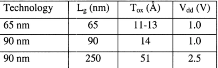
2.1 Key device and process parameters for the four device types in this thesis
28
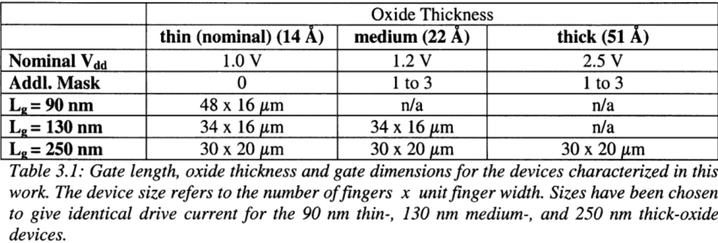
3.1 Gate length, oxide thickness and gate dimensions for the devices characterized in this work. The device size
refers to the number offingers x unit finger width. Sizes have been chosen to give identical drive current for the 90 nm thin-, 130 nm medium-, and 250 nm thick-oxide devices.
36
3.2 Performance comparison of standard 90 nm device and a parallel combination of 8 standard devices.
Impedances were optimized for the best linearity-efficiency tradeoff.
36
4.1 Overview of the devices used in this chapter, fabricated in either 65 or 90 nm technologies. The gate length
refers to the equivalent polysilicon half pitch dimension.
49
5.1 Model parameters extracted from DC measurements, for the 65 nm and 90 nm technologies.
Chapter 1.
Introduction
This work will perform a detailed comparative study of the RF power potential of CMOS
technology. The broader context of this research is the attractiveness of using logic CMOS as a
platform for wireless system-on-chip applications. This enables true single-chip solutions for
portable wireless systems with significant consequences in form factor and module design. Logic
CMOS is the ideal platform for system-on-chip integration. Logic CMOS is the lowest cost
technology, and the digital baseband in wireless systems is already being implemented in logic
CMOS. CMOS modeling, simulation, design and verification tools are very mature and broadly
available. Additionally, CMOS designs port relatively well from fab to fab and generation to
generation. Particularly important for RF wireless systems, great progress has been shown
recently in enabling RF functions with CMOS. Not surprisingly, there is a lot of interest in
exploring the RF potential of logic CMOS.
The microelectronics industry is striving to reduce the cost, complexity, and time to market of
wireless systems through single-chip integration of mixed-signal RF/digital functions. Achieving
such integration, while minimizing the increased cost of technology add-ons, places high
demands on the base CMOS technology. In this regard, the integration of the power amplifier
(PA) function remains a particular challenge as technology geometries scale down.
Over the past decade, silicon technology has made a strong entry into the RF power amplifier
field. Figure 1.1 shows the growth of silicon and CMOS in published research on device
technologies for RF power amplifiers. In the commercial sector, CMOS has captured substantial
market share for RF power amplifier applications. These include portable wireless systems, such
as bluetooth and wireless LAN. The use of CMOS is because of cost and integration pressure.
With cost a central issue in most high-volume applications, the digital portions of these
applications will continue to be scaled down. As one example, the migration of CDMA chipsets
onto 65 nm started in 2005. While this migration takes place only for the digital chips, it shows
that any future integration requires the analog/RF chips to be implemented in deeply scaled
technologies.
Through a combination of detailed RF power characterization and analysis, in this thesis, we
will study the RF power performance of deeply scaled CMOS, and determine its performance
limits. We focus on conducting as opposed to switching type amplifiers. We will consider both
the standard digital devices of each node, as well as available 1/O (thick gate oxide) devices. The
answers to this study are necessarily complex because this is a multidimensional space: power
level, frequency, linearity, power efficiency and reliability.
1.1.
Literature Background: State of the Art
To better illustrate the role of CMOS in RF power amplifiers, we have conducted a literature
study of IEEE publications concerning power amplifiers operating in the RF above 900 MHz.
Fig. 1.1
Number of power-amplifier research results published in IEEE journals and conferences in
1993 (top) and 2003 (bottom), by material and device types. In 2003, 16% of the overall activity
was taking place in CMOS technology. [31-1006]
The growing importance of silicon based power amplifiers can be seen in Figs. 1.1 and 1.2.
Between 1993 and 2003, the portion of silicon based power amplifiers in publications has taken a
substantial share of the overall PA research. CMOS based power amplifiers make up about 50%
of the PA activity taking place in silicon today (Fig. 1.2b). Clearly offering the cheapest and
most integratable technology, CMOS also is able to deliver performance at low voltages [1]. Fig.
1.3 shows the power density as a function of the bias voltage for a variety of semiconductor
technologies. CMOS is competitive with respect to the other technologies such as GaAs HEMT
and MESFETs, up to about 3 Volts. With the sharp increase in portable consumer electronics
operating at frequencies below 5 GHz and voltages below 3V, CMOS has become an important
mostly focused on circuit design techniques, such as linearization techniques and integrated
transceivers [2-4]. Much less research has been done on CMOS technology itself [5-7]. This is
the object of this work.
The trend towards scaling of RF power CMOS is apparent from Figs 1.4-1.6. Over time,
publications concerned with power CMOS have continued to follow the CMOS roadmap and
used shorter gate lengths (Fig. 1.4). There are two important reasons why scaling makes sense.
First, as the gate length is scaled down, operation at higher frequencies is possible (Fig. 1.5). In
addition, scaling holds benefits even if the frequency of operation is not changed, as shown in
Fig. 1.6. Due to the increase in transconductance and power gain that comes with shorter
channels, scaled devices achieve higher power added efficiency and improved performance [1].
Inn - Research Activity in Silicon
40 - by Device Type - N Si BJT 30- SiGe HBT SS LDMOS S CMOS 20-> 75-o.
S50-0
25
0- a- 10-E YearFig. 1.2a (left), 1.2b (right)
Research activity as a function of time
type. [31-1006]
by material (left) and within silicon (right) by device
4 r~r. IUU E 10
E
, 0.1 -o0..
0.001 0.0001 0.1 Si 0 0 10 100Vdd
[V]
Fig. 1.3
Power density as a function of bias voltage. Boundaries of different materials and device types
are shown. CMOS is able to operate at voltages below 5 V, and demonstrates power densities
comparable to the other materials. [31-1006]
CMUS Scaling 0 o o 0.35 pm 0o o o o *-- 0.25 pm S -- 0.18pm So- 0.13 pm - 90 nm 1990 1995 2000 2005 Year
Fig. 1.4
Physical gate length of CMOS power devices and amplifiers, as a function of time, for IEEE
published research. The trend towards scaling the gate exists even in RF power CMOS, as the
data suggests. The CMOS technology nodes are marked by the arrows. Shorter gates generally
result in higher gain (through transconductance) and therefore better efficiency and
performance
-
though at the cost of reduced bias voltage and output power (see Fig. 1.3, 1.5).
I U.UU
1.00
- 0.10
0.01
-.
~
f-lg ¢• 0 "-. 06 4,, 0 4, o o 4, 1.0 Frequency [GHz]Fig. 1.5
Physical
amplifiers.
the data.
60
.40( 20
0
gate length as a function of operation frequency for CMOS RF power devices and
Device operation at higher frequencies requires a shorter gate, as can be seen from
Impact of Scaling on Efficiency
(27
GHz
<
freq
< 50 GHz)
0.4
0.6
LG [um]
Fig. 1.6
Impact of gate length scaling on power added efficiency in a selected frequency band.
Efficiency improves with shorter gates, due to higher transconductance and improved gain and
frequency response. Data includes MESFET and HEMT based amplifiers.
IU.00 1.00 0.10 0.01 10.0
8
I6
4,1Q
4,S
0.0
0.2
0.8
1.0
· i ~n nn-1.2.
Application Space for Power Amplifiers
Two of the most important requirements for a power amplifier are the output power
level and the frequency of operation.
We would like to illustrate the application
demands on these two parameters. Fig. 1.7 shows this, by sketching the current RF
power application landscape into the frequency-power space. The applications span
1-100 GHz in frequency, and 10 mW to 1-100 W in output power level. Because of this
broad range of frequencies and power levels, no single one technology dominates this
space. In Fig. 1.8 we overlap technologies shown in the previous section (Fig. 1.1) onto
this space. Silicon based technologies dominate the low frequency space, with CMOS
occupying the low power, low frequency corner. LDMOS devices are suitable to higher
power levels, and SiGe HBTs allow for higher frequencies.
100 10 1 0.1 A A 10 Frequency [GHz]
Fig. 1.7
Overview of the different applications that require RF power. The sketch shows the broad range
offrequencies and power levels that are required in different applications.
100 10 1 0.1 U.V I 10 Frequency [GHz]
Fig. 1.8
Technology landscape in the frequency-power space. Silicon based technologies occupy the low
frequency regions, while compound semiconductors are used for higher frequencies and power
levels.
100 1000
100 1000
1.3.
Thesis Goals
This thesis is attempting to develop fundamental understanding about the RF power potential
of logic CMOS. Through a combination of detailed RF power characterization and analysis, we
wish to answer the following questions:
* What is the RF power potential of logic CMOS?
* How does the RF power performance of CMOS evolve
as the technology is scaled down the road map?
* What is the impact of device layout on RF power performance?
The answers to these questions are necessarily complex because this is a multidimensional
space: power level, frequency, power efficiency, layout considerations and device biasing
choices.
Fig. 1.9. illustrates this goal. We would like to identify the boundary of RF CMOS to
accomplish the power amplifier function, both in terms of frequency and output power. In
addition, the goal is to identify methods to push out these boundaries.
We will accomplish the goals mentioned in the introduction by studying a variety of aspects
which combined will give an excellent insight into RF power capability of deeply scaled CMOS:
A
Technology
Our evaluation will focus on the 90 nm and 65 nm nodes. We will study different device options
0.13 tm and 0.25 tpm devices), variation of gate length, and device layout variations. The
analysis will include measurement of power and efficiency. This will then enable us to quantify
the tradeoffs between the standard CMOS devices and more complex but potentially better
performing alternative devices.
B
Technology Scaling
By including various oxide thicknesses on a 90 nm wafer, we are essentially able to study
devices of the 90 nm, 130 nm and 250 nm nodes. In addition, devices from a 65 nm wafer allow
us to also study the 65 nm node. These two wafers give us a wide range of different technologies
along the CMOS roadmap. The impact of scaling on power added efficiency and output power
for conduction type amplifiers will be studied.
C
Layout Design
We will develop new device layouts to improve RF power performance. Important
considerations for developing RF power layouts are RF and DC parasitic concerns. The impact
of the layouts on performance and frequency response will be investigated.
D
Power Capability
We will study the ability of the technology to produce high output power by studying how device
size relates to performance. The output power can saturate with device size for several reasons,
such as gate resistance, self heating, inefficient power combining, and impedance mismatches.
We will study a wide range of device widths that should allow us to identify the limiting factors.
Different options of achieving large devices will be studied: changes in the device aspect ratio
(number of fingers / unit finger width), changes in total device width, and the effectiveness of
E
Frequency Capability
We will study how the performance degrades with frequency, as we approach fmax. This study
will not only show the range of frequency operation for the device, but also establish a relation
between fmax and a frequency giving acceptable device performance (e.g. good gain and PAE).
F
Modeling
In order to better understand the behavior of the observed power measurements, we will develop
a simple, physics based device model. The model should capture the major dependencies
observed in the data, and help in estimating the capabilities of the different CMOS technologies.
1.4.
Outline
We will start by a brief description of the experimental setup in Chapter 2. This includes the
device layout, and the notations used to describe it, as well as the experimental setup for
performing the different measurements.
Chapter 3 will discuss the performance of 90 nm
devices, and studies the impact of gate oxide and gate length scaling.
It compares the
performance of 90 nm, 130 nm and 250 nm technologies. Chapter 4 studies the performance of
65 nm devices, and also addresses the question of output power scaling. It shows the importance
of device layout when scaling output power. A simple device model is developed in Chapter 5,
which allows us to describe all the major trends seen in Chapters 3 and 4. We will combine all
the results from the measurements and models in Chapter 6, which aims at illustrating the power
I
-10
r--1:
ac
0.1 0.01SAT
a.Deeply
Scaled
• CMOS
"Performance
: Space
i... m a i i ... HI
, -- - , - I , , I I I I I I 1 ' I I I I I I I10.1
1
10
100
1000
Frequency [GHz]
Fig. 1.9
Illustration of how RF CMOS devices exhibit limitations of power and frequency. The
goal of
this thesis is to identify these limits, and study how they can be pushed out.
4 hh#'
Chapter 2.
Experimental
This chapter describes the devices and technologies used, as well as the types of experiments
carried out on them. I will first describe the device technologies used and the types of devices. I
will then broadly describe the three types of characterizations carried out on the devices: DC,
S-parameter, and RFI power characterization. All measurements were performed on-wafer using
standard RF probes (ground-signal-ground).
2.1.
Technology Description
The technology that has been studied in this work is a foundry 90 nm and 65 nm CMOS
technology manufactured at IBM [6]. Table 2.1 shows the different devices fabricated. We will
label these devices by their ITRS equivalent technology node: Lg,inn = 65 nm, 90 nm, 130 nm
and 250 nm, with the understanding that the physical gate length will be below those values,
particularly at the 90 nm node. The 65 nm wafer has devices with a nominal gate oxide thickness
between 11 and 13
A
and Lg,min = 65 nm (Vdd = 1.0 V). For the 90 nm wafer, in addition to the
standard 90 nm NFET
(Lg,min =
90 nm) with a nominal gate oxide thickness of 14
A
(Vdd = 1.0
V), there is an intermediate oxide I/O FET (tox = 22
A,
Lg,min = 130 nm) equivalent to a standard
equivalent to that of the 250 nm node
(Vdd
= 2.5 V). Depending on the process details, the
additional mask count required to offer the I/O device options is between 1 and 3.
The 90 nm devices were taped out May 2003, when the technology was ramped up for
production. The 65 nm devices were taped out in August 2004, at which stage the
technology was still undergoing development. The presence of the I/O devices allowed
us to compare the performance of essentially four different CMOS technology nodes (65
nm, 90 nm, 0.13 ýtm and 0.25 Fam). The 0.13 [am medium oxide device, however, is not
completely independently optimized. It shares some process steps with the nominal
thin oxide 90 nm device. Therefore, it does not truly represent a 0.13 ý.m node, and its
performance may differ. Table 2.1 highlights the key process parameters for these
technologies:
Parameter
65 nm
90 nm
130 Ipm
0.25 ýtm
on 90 nm wafer on 90 nm wafer
ITRS Equivalent Node, Lgmin
65 nm
90 nm
0.13
tm
0.25 pm
Physical
Lphysical
40
nm
63
nm
120
nm
240 nm
Oxide Thickness
11-13
A
14
A
22
A
52
A
Nominal Voltage
1.0 V
1.0 V
1.2 V
2.5 V
Standard Cell
(NFxWG,F)64x12 pm 48x16 pm 34x16 pm
30x20
pm
Table 2.1. Key device and process parameters
for
the four device types in this thesis
2.2.
Device Layout
We have fabricated devices with a variety of layouts providing a broad range of total device
widths. The unit cell dimensions were given in Table 2.1. In general, the device layout consists
number of parallel device cells (Nc), times the number of device fingers (NF) per cell, times the
unit finger
width (WG,F).
We will label devices as
WG,TOT = NC X NF x WG,F.
Because the device fingers are very wide, electromigration concerns can arise due to the high
current densities. A standard multi-finger device layout was modified to allow for better current
flow in and out of the drain/source contacts, reducing the peak current within the device
metallization layers. The layout uses a double-sided gate access to the device, as well as a
double sided source access. The drain is routed out vertically. This metallization is done with 4
levels of metal. Thicker levels are then used to route the gate, source and drain to the RF pads.
An illustration of the device layout is shown in Fig. 2.1.
plane of
symmetry
Fig. 2.1
Vertical drain layout (source
=
red, drain
=
blue, gate=green). The structure is symmetric, and
only half is shown. The symmetry plane is indicated. The layout design is patent pending.
2.3.
DC and S-Parameter Characterization
Measurements of the devices under DC conditions were performed at MIT using an HP4145B
parameter analyzer. A sample Id-Vds sweep is shown in Fig. 2.2. This data was taken for the
standard 90 nm device. S-parameter measurements were performed at IBM, on an automated
probe station up to 80 GHz. From the S-parameter measurements, ft and fmax estimates were
extracted. A typical S-parameter measurement result is shown in Fig. 2.3, for the 90 nm standard
device.
400
300
200
100
0
0
1
2
3
Vds
[V]
Fig. 2.2
DC sweep for the standard 90 nm device (1x48x16 tim), with Vgs from 0.4V to 1V in 0.1V steps.
The DC measurements exhibit self-heating, which can be seen by the higher Ro as Vgs increases.
Therefore, the Ro values seen in DC measurements for high Vgs and Id will differ slightly from
those relevant to the RF operation of the device.
50x S12
D
Fig. 2.3
S-parameters (0.5-50 GHz) for the standard 90 nm device (lx48x16 pIm), biased at Vds=lV,
Vgs=0.58V. S11 and S22 are plotted on the left, and S21 and 50 times S12 are plotted on the
right.
2.4.
Power Characterization
RF power characterization was carried out primarily at 8 GHz on a Maury load-pull system.
We chose 8 GHz for the bulk of our work to explore the high-frequency potential of deeply
scaled CMOS technologies. Measurements at higher frequencies also avoid device oscillations.
The higher the gain, the more susceptible the device becomes to oscillations. If the impedances
are tuned to maximize the gain at a high frequency, they will typically present a mismatch at
lower frequencies. As the gain drops with frequency, this helps to flatten the gain vs. frequency
behavior. This helps to avoid very high gain values at any frequency, and therefore reduces the
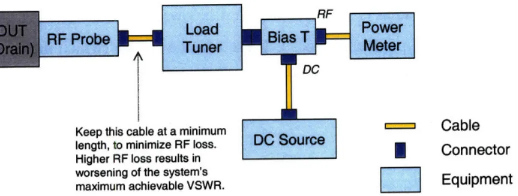
risk of oscillations. The measurement theory and system design is described in more detail in
Appendices A and B. The system creates a single RF frequency that is applied to the gate.
RF input and output power as well as the bias currents are measured, and allow computation of
the relevant figures of merit (Id, PAE, Gain,
Pout, Pin).
Power measurements were optimized for peak PAE, by alternating source- and load-pull
measurements backed off a few dB from the input power level giving peak PAE. This
optimization was repeated for each change of device setup variables (for example, when
measuring the same device at different values of
Vdd).
A typical power measurement sweep is
shown in Fig. 2.4. As the device enters compression, the grain drops, while the output power
saturates. The PAE is defined as
PAE=
out-
Pin Pout(Gain
- 1)
Eq.
2.1
Pdc
Pd,
Gain
=P
c
where
Pin
and
Pout
is the RF power in and out of the device, and PDc is the DC power into the
device. As the input power is increasing, the PAE will rise. However, in compression the gain
drops as the output power is saturating. This will eventually result in the PAE beginning to drop,
reaching a maximum PAE typically between 1-5 dB in compression.
Often, we performed a series of power sweeps with one variable changing (e.g. frequency).
The results of this series of sweeps were reported as the peak PAE and output power at peak
PAE of each of the power sweeps.
Separately, we also performed linearity measurements for the standard 90 nm device at 2.2
GHz on an ATN load pull system, at IBM.
Throughout this thesis, we will be quoting the bias condition as a combination of
Vds
and Id.
The value of
Id
is the DC drain current without the presence of input power. This current is
achieved with a gate bias Vg. During the power measurement, this gate bias is held constant,
rather than the actual
Id
value. In conduction type amplifiers, it is common to observe that as the
input power is increased, the DC drain current measured into the device will also increase. The
origin of the self biasing is the non-linearity that enters when the input signal swings below the
device's threshold voltage [30]. While the average Vg remains at its bias value, swinging the
input below Vt will not result in a negative drain current, but rather in zero current. This
introduces the asymmetry. While a swing to higher Vg will result in higher drain current,
swining Vg below Vt will not result in less (more negative) drain current. Therefore, the average
DC current increases, despite the fact that the average voltage on the gate is unchanged.
70
60
50
40
30
20
10
0
PAE
-10
-5
0
5
Pout
[dBm]
10
15
20
Fig. 2.4.
A typical power sweep, showing the power added efficiency (PAE) and the transducer gain, as a
function of the measured output power. This measurement shows the 65 nm standard device
(768 im width), at 4 GHz in class AB bias.
Chapter 3
90 nm Technology
The technology that has been studied in this work is a foundry 90 nm CMOS technology
manufactured at I]BM [8]. In addition to the standard 90 nm NFET with a nominal gate oxide
thickness of 14
A
(Vdd
=
1.0 V), there is an intermediate oxide I/O FET (tox
=
22
A)
equivalent to
a standard 130 nmn node logic device (Vdd
=
1.2 V), and a thick oxide I/O FET (tox
=
51
A)
equivalent to that of the 250 nm node (Vdd
=
2.5 V). Additionally, devices with three different
gate lengths are available. We label these by the half pitch of their equivalent technology node:
90 nm, 130 nm and 250 nm, with the understanding that the physical gate length will be below
those values, particularly at the 90 nm node. Not all combinations of oxide thickness and gate
length are implemented. Table 3.1 gives all available device options. Depending on the process
details, the additional mask count required to offer these device options is between 1 and 3.
We have fabricated devices with a variety of layouts providing a broad range of total device
widths. The unit cell dimensions are given in Table 3.1. In general, the device layout consists of
several multi-finger device cells in parallel. The total device width (WG,TOT) is the product of a
number of parallel device cells (Nc), times the number of device fingers (NF) per cell, times the
Nominal
Vdd
Addl. Mask
L, = 90 nm
L,= 130 nm
L, = 250 nm
Oxide Thickness
thin (nominal) (14 A)
medium (22 A)
thick (51 A)
1.0 V
1.2 V
2.5 V
0
1 to 3
1 to 3
48 x 16 jm
n/a
n/a
34 x 16 tm
34 x 16 tm
n/a
30 x 20 /m
30 x 20 m
30 x 20 m
Table 3.1: Gate length, oxide thickness and gate dimensions for the devices characterized in this
work. The device size refers to the number offingers x unit finger width. Sizes have been chosen
to give identical drive current for the 90 nm thin-, 130 nm medium-, and 250 nm thick-oxide
devices.
90 nm Standard
lx48x16 /m
8x48x16 im
Device
Bias
Vdd = 1 V
Vdd = V
Id = 25 mA
Id = 200 mA
Frequency
2.2 GHz
2.2 GHz
Peak PAE
66 %
59 %
Pout
at peak PAE
12.5 dBm
20.2 dBm
Small signal gain
21.2 dB
14 dB
OIP3
25 dBm
30 dBm
PAE at IM
3=-35dBc
14 %
12 %
Pot at IM
3=-35dBc
6 dBm
12 dBm
Pout at 1 dB
11 dBm
18 dBm
compression
Table 3.2: Performance comparison of standard 90 nm device and a parallel combination of 8
standard devices. Impedances were optimized for the best linearity-efficiency tradeoff
Power measurements were optimized for peak PAE, by alternating source- and load-pull
measurements backed off a few dB from the input power level giving peak PAE. This
optimization was repeated for each change of device setup variables (for example, when
measuring the same device at different values of
Vdd).
Separately, we also performed linearity measurements at 2.2 GHz on an ATN load pull system.
3.1. Results
We will first discuss the RF power performance of the standard logic device (thin oxide, Lg=
90
nm), followed by a discussion of the performance impact of other device options that involve
scaling the gate oxide thickness (tox) and gate length (Lg). In the following section we discuss the
physical origin of the various results that have been obtained.
3.1.1.
RF Power Performance of the 90 nm Logic Device
The
2.2
GHz power performance of two standard digital 90 nm devices (biased at
Vdd=1 V)with different total[ gate widths is shown in Fig. 3.1, and summarized in Table 3.2. We compare
the performance of a single cell device (1x48x16 Im) to that of another device consisting of
70 60 ,.50
< 40
M 30 20 10 0 0 -20 -40 -60 -80 -100 -30 -20 -10 0 Pout [dBm] 10 20 30Fig. 3.1
Power performance at 2.2 GHz of a thin-oxide 90 nm device (1x48x16 /Am) and a device array
(8x48x16 iLm), both biased at
Vdd =
1 V and Id
=
26 mA/mm. Impedances were optimized for the
best linearity-efficiency tradeoff.
eight of these cells wired in parallel (8x48x16 Am), giving an eightfold increase in
WG,TOT.For
the 1x48x16 Am device, a peak PAE in class AB operation of about 66% is obtained at an output
power of 12.7 dBm (18.6 mW, or 24.2 mW/mm). The 8x48x16 Am device achieved a peak PAE
of 59% at an output power of 20.2 dBm (104 mW, or 17.0 mW/mm), indicating a good scaling
of Pot with cell count. A slight decrease in PAE, power gain and output power density can be
seen. This indicates that an upper limit on power scaling exists. The PAE at linearity (in terms of
IM
3) of -35 dBc is 14% and 12% for the lx48x16 Am device and the 8x48x16 Am device,
respectively.
To put these results in context, a WCDMA power amplifier driver requires about 14 dBm at 1
dB compression power, with an OIP
3of 24 dBm [9]. From Table 3.2 we see that the 8x48x16
Am device exceeds these requirements by a safe margin. The results of Table 3.2 suggest that 90
nm CMOS is quite suitable for a wide range of integrated PA
D IV0
80
-0
w
6 0
-c
40
-21.
200
-'out Air= 1x48x16)V
dd=1 V, Id = 2 6 rA/mmI
I
I
m
10
.0
-5
,"
0
-0
0
5
10
15
20
Frequency [GHz]
Fig. 3.2
Peak PAE and output power at peak PAE as a function of frequency for the standard 90 nm
device (1x48x16
ALm).
All measurement points were taken at Vdd =
V,Id = 26 mA/mm, and
impedances were reoptimized at each frequency. The output power is roughly independent of
frequency, while the peak PAE is dropping as the frequency increases.
applications, such as WLANs, bluetooth and cellular PA drivers, giving acceptable efficiency
under linear conditions.
Measurements at 8 GHz for the standard 90 nm thin-oxide device at Vdd = 1 were also
performed. The standard device (1x48x16 rim) achieved a peak PAE of 56.8% at 13.4 dBm (21.9
mW, or 28.5 mW/mm) output power with an associated gain of 14.6 dB. These results at 8 GHz
are slightly better than the performance reported at
2.2
GHz above. This is due to using a
different measurement system that is able to present a better source and load match.
We have also measured the power performance of the standard device (1x48x16
rpm) as a
function of frequency. The results are shown in Fig. 3.2. The output power is constant with
frequency over a broad range, while the peak PAE is dropping with frequency. Operating the
device at higher frequencies reduces the power gain and results in lower peak
PAE.
Across-wafer uniformity measurements of 18 devices were also performed. These
measurements were carried out with constant impedances, input power and bias points (Vdd
=1
V,
ld
=
26 mA/mm) at 8 GHz. The data includes both the probe contact uncertainty as well as the
device variation across the wafer. The device geometry used was lx96x8 Jim. Excellent
uniformity was obtained across the entire 8" wafer, with a measured PAE of 59.3%±0.6%, and
an output power of 14.2 dBm ± 0.1 dB, as well as a small signal gain of 16.3 dB ± 0.3 dB. This
3.1.2.
RF Power Performance of Other Device Options
We have studied the RF power suitability of the different device options as a function of the
drain bias, Vdd. This provides a fair performance comparison as the different devices will show
optimal operation at different voltages.
Fig. 3.3 compares in detail the peak PAE power performance of the thin oxide devices for the
three different gate lengths, as a function of Vdd at 8 GHz (Id
=
26 mA/mm). The graph shows the
small signal gain, the peak PAE and the corresponding output power density normalized to a 1
mm device width. At any one value of Vdd, there is not much difference between the 90 nm and
the 130 nm devices, while the 250 nm device gives much lower performance. As Vdd increases,
--- Lg=90nm PAE - Lg=130nm - -Lg=250nm
-vdd7
freq = 8 GHz Id = 26 mA/mmrr5:- ifW thin oxide I I i i i I0.1
1.0
10.0
Vdd
[V]
Fig. 3.3
Gain, PAE and output power density at peak PAE point as a function of Vdd for thin oxide
devices of three different gate lengths at 8 GHz. Impedances and input power drive were
re-optimized at each Vddfor each device.
7u -
--o
60-0) 50
-a
40
-Em
S30-
30
-<
20
C
1
) 10-0
IUUV100
E
-100.C
E
1
1
Iu
"
60-C ,"
50-E
MAO
S20
-0
-c--Thin Oxide -- Medium Oxide - Thick( freq = 8 GHz - .Vdd 2 Id = Z6 mA/mm lx30x20 pm L.g = 250 nm i i i , i ii l l , i iIVVV
100
10
C.1
0.1
1.0
10.0
Vdd [VI
Fig. 3.4
Gain, PAE and output power density at peak PAE as a function of Vdd for 250 nm devices with
three different gate oxide thicknesses at 8 GHz. Impedances and input power drive were
re-optimized at each Vddfor each device.
all devices show a higher output power density. The dependence is quadratic, and agrees with the
behavior seen in chapter 1 (Fig. 1.3). The gain at peak PAE changes only slightly with Vdd and is
not very different from one device to the other. For the 90 and 130 nm devices, the peak PAE is
rather flat across a broad range of Vdd. The 250 nm gate length devices, however, not only show
a much lower peak PAE, but the PAE starts to rapidly drop as Vdd is reduced. The performance
of the Lg=250 nm devices is limited by the low voltage capability of the thin oxide. We discuss
the physics of this in section 4.
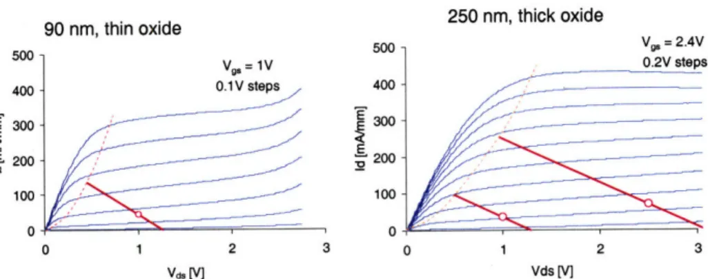
Fig. 3.4 shows the impact of gate oxide thickness, keeping Lg constant at 250 nm. Decreasing
the oxide thickness without changing the gate length results in lower gain and lower PAE.
However, the power density for a given Vdd is increasing slightly. The reason for this is
discussed in Section 4.
---- Lg=90nm, Thin Ox ---- Lg=130nm, Med Ox -L-- l=250nm, Thick Ox ,",-Vdd2
70
-60
-50
-40
-30
-
20-10
-1.0
Vdd
[V]
Fig. 3.5
Gain, PAE and output power density at peak PAE point as a function of
Vdd
when scaling both
Lg and gate oxide thickness at 8 GHz. Impedances and input power drive were re-optimized at
each Vddfor each device.
S-60
-50
-40
-Vdd
=1
V
Vdd
=
2.5
V
90 nrr thin o:10
100
1000
Output Power Density [mW/mm]
Fig. 3.6
Comparison of the 90 nm thin and 250 nm thick oxide devices. Both devices can achieve similar
peak PAE levels, though at different operating voltages and power densities, as indicated.
freq = 8 GHZ Id = 26 mA/mm