Deeply-Scaled GaN High Electron Mobility Transistors
for RF Applications
by
Dong Seup Lee
B.S., Electrical Engineering Seoul National University, 2007S.M., Electrical Engineering and Computer Science Seoul National University, 2009
AROMV ES
MASSACHUSETTS INS117T EOFTECHNOLOGY
APR 10 2014
H-S
§
Submitted to the Department of Electrical Engineering and Computer Science in Partial Fulfillment of the Requirements for the Degree of
Doctor of Philosophy at the
Massachusetts Institute of Technology February, 2014
C 2014 Massachusetts Institute of Technology. All Rights Reserved.
Author
Department of Electrical Engineerj and Computocience January 21, 2014
Certified by
T s Palacios Associate Professor of Elec ical Engineering Thesis Supervisor
Accepted by
s le A. Kolodziej ski Professor of Electrical Engineering Chairman, Department Committee on Graduate Students
Deeply-Scaled GaN High Electron Mobility Transistors
for RF Applications
by
Dong Seup Lee
Submitted to the Department of Electrical Engineering and Computer Science On January 21, 2014 in Partial Fulfillment of the Requirements for the Degree of
Doctor of Philosophy
ABSTRACT
Due to the unique combination of large critical breakdown field and high electron velocity, GaN-based high electron mobility transistors (HEMTs) have great potential for next generation high power RF amplifiers. The performance of GaN devices has increased continuously in the last two decades. However, in spite of the improvements, there are still several critical issues limiting the high frequency operation of these devices. One of the key challenges is the lower-than-expected maximum current gain cutoff frequency (fT) of deeply-scaled GaN HEMTs. The fT
of the short channel devices is well below both projections from maximum frequency in the long channel devices and theoretical expectations based on material properties. Another important issue is a roll-off of the device frequency performance under wide bias range, which limits the large-signal high speed operation in the deeply-scaled devices. This thesis focuses on these two important problems and investigates them both analytically and experimentally. First, through systematic study of the transistor delay, the critical factors limiting intrinsic and extrinsic device speed are clarified and several technologies are demonstrated to overcome these limits. This has allowed the demonstration of state-of-the-art high frequency performance GaN HEMTs. Second, in order to understand the origin of the decrease in device speed at high drain and gate bias, a new extraction method and novel transistor structure have been developed, which provide an excellent guide for future device optimization.
Thesis supervisor: Tomis Palacios
ACKNOWLEDGEMENT
The past four and half years in MIT have been a very important period in my life, which allows me to become both better researcher and more mature person. As this has been possible thanks to help of outstanding people, it is my great pleasure to acknowledge them here.
First, I am deeply indebted to my advisor, Prof. Tomas Palkicios. His scientific insight, consistent support, and endless encouragement have always motivated me to focus on research and enabled me to overcome challenges. Also, I have learned about many other aspects from him, including his kindness and politeness. It has been my great fortune to be his student and he will be my model for future.
Second, I would like to express my sincere gratitude to my thesis committee, Prof. Jesus del Alamo and Prof. Judy Hoyt for their invaluable advices and comments. Measurement and analysis methods developed in Prof. Jesus del Alamo's group have been an important foundation in my research. Also, Prof. Judy Hoyt has always encouraged me with excellent suggestions. Thanks to their help, I have been able to make my thesis more complete.
Thirdly, although not in my committee, I would like to thank Prof. Dimitri Antoniadis in MIT and Prof. Patrick Fay in Notre Dame University. With his vast knowledge of device physics and modeling, Prof. Dimitiri Antoniadis has given excellent advices and guides. Also, Prof. Patrick Fay has helped me for high frequency measurements and shared his knowledge and insight on microwave characterization with me.
I would like to acknowledge DARPA NEXT program monitored by Dr. John Albrecht, which has continuously supported this work. In addition, I am grateful to Triquint and IQE for their close collaboration for this project. I also want to express my gratitude to Samsung Scholarship for its financial support for my Ph. D. years.
I am also thankful to all my colleagues in Palacios's group. Former group members, Han Wang and Jinwook Chung taught me device fabrication methods and measurement skills, which allowed me to start my research smoothly. Bin Lu, Daniel Piedra and Min Sun were always happy to share their knowledge on power electronics and help my process. Omair Saadat and Allen Hsu helped me a lot with low temperature measurement and program setup. I also enjoyed discussion with Feng Gao and Mohamed Azize on device reliability and film growth, respectively. Yuhao Zang helped me with simulation setup and I learnt about two-dimensional material systems from Xu Zhang and Lili Yu. Also, Dr. Kevin Kyungbum Ryu and Dr. Hyung Seok Lee gave me many good advices and shared their research experiences. Dr. Tatsuya Fujishima helped me to learn InN process and I enjoyed discussion with Dr. Elison Matioli and Dr. Puneet Srivastava on RF devices. I thank all other former and present group members including Benjamin Mailly, Tadahiro Imada, Sameer Joglekar, Cosmi Lin, Charles Mackin, Ahmad Zubair, Dr. Zhihong Liu, Dr. Takamichi Sumitomo, Dr. Alexandre Rocha Paschoal, Dr. Marco de Fazio, and so on. Also, I would like to express my appreciation to Joseph Baylon and Elizabeth Kubicki for their administrative assistance. Moreover, I should not forget the other sixth floor fellows and MTL staffs for their friendship and help.
Finally, my sincere gratitude goes to my family for their love and support. My lovely wife Yeonyoon Jeong has always supported me with love. This thesis is dedicated to them.
Contents
C hapter 1. Introduction... 22
1.1. N itride-based sem iconductors... 22
1.2. GaN transistors...24
1.3. Issues in GaN RF devices...29
1.3.1. Low m axim um device speed...29
1.3.2. Roll-off of the device frequency perform ance at high biases... 30
1.4. Project goal and thesis outline... 31
Chapter 2. Basic Device Design and Physics in GaN HEMTs...34
2.1. Polarization in GaN-based heterostructures... 34
2.2. Fabrication process of GaN HEM Ts...37
2.3 DC characteristics of GaN HEM Ts... 40
2.4. RF characteristics of GaN HEM Ts... 41
Chapter 3. Intrinsic Device Limits for Maximum GaN HEMT Speed...48
3.1. Introduction...48
3.2. Lim iting factors in the intrinsic GaN transistor... 50
3.2.1. Analysis tools to study device speed... 50
3.2.2. Intrinsic delay...52
3.3. Gate length scaling...53
3.3.1. Electron-beam lithography technology ... 53
3.3.2. Issues in deeply-scaled AlGaN/GaN HEM Ts... 56
3.4. Top barrier engineering... 59
3.4.1. Gate m odulation efficiency... 59
3.4.2. InAlN/GaN heterostructure... 60
3.4.3. Device fabrication... 61
3.4.4. DC characteristics... 63
3.5. Channel charge confinem ent... 67
3.5.1. Pinch-off and subthreshold characteristics... 67
3.5.2. InAiN/G aN HEM Ts with AlGaN back barrier... 68
3.5.2.1. AlGaN back barrier heterostructure... 68
3.5.2.2. Device fabrication... 71
3.5.2.3. Im pact of AlGaN back barrier... 72
3.5.2.4. Deeply-scaled InAIN/GaN HEMT with AlGaN back barrier...74
3.5.3. InAIN/GaN HEM Ts with vertical channel scaling...76
3.5.3.1. Heterostructure for vertical channel scaling... 76
3.5.3.2. Device fabrication... 79
3.5.3.3. DC characteristics... 80
3.5.3.4. RF characteristics... 83
3.5.3.5. Vertical channel scaling design... 87
3.6. Conclusion...88
Chapter 4. Extrinsic Limits for Maximum GaN HEMT Speed...90
4.1. Introduction...90
4.2. Parasitic delay...91
4.2.1. Origin of the parasitic delay... 91
4.2.2 Low temperature m easurem ent... 94
4.2.3 GaN HEM Ts with ultra-low on-resistance...96
4.2.3.1 Technologies to reduce source/drain resistances... 96
4.2.3.2. Device fabrication... 97
4.2.3.3. DC characteristics... 98
4.2.3.4. RF characteristics...100
4.3. Extrinsic delay...103
4.3.1. Im portance of extrinsic delay...103
4.3.2. Device fabrication...104
4.3.3. Passivation effect on DC and pulsed-IV characteristics...105
4.3.4. Passivation effect on RF characteristics...108
4.4. Projection of fT in deeply-scaled GaN HEMTs ... 115
4.5. Conclusion...118
4.5. Conclusion ... 118
C hapter 5. D elay under H igh D rain B ias: D rain D elay ... 120
5.1. Introduction...120
5.2. Drain delay extraction...122
5.2.1. D rain delay extraction m ethod in literatures...122
5.2.2. Small-signal equivalent circuit model including drain delay effects...124
5.2.3. Com parison to other extraction m ethods...129
5.3. Drain delay in short channel devices...131
5.3.1. H igh extracted drain delay rate...131
5.3.2. Suppression of gm.int degradation at high drain bias...134
5.3.3. Scaling gate-to-drain spacing ... 136
5.4. Conclusion...140
Chapter 6. Nonlinearity of Deeply-Scaled GaN HEMTs...142
6.1. Introduction...142
6.2. N onlinearity of gm in GaN HEM Ts...143
6.2.1. Current understanding in the literature...143
6.2.2. Self-aligned GaN H EM Ts...145
6.3. N anow ire channel GaN HEM Ts...146
6.3.1. Lim itation of source access region... 146
6.3.2. D evice structure...148
6.3.3. D evice fabrication...149
6.3.4. D C characteristics...152
6.3.5. Effect of channel w idth and w idth ratio... 156
6.3.6. Surrounding gate effect...159
6.3.7. RF characteristics...160
6.3.8. Breakdow n voltage...161
C hapter 7. C onclusion and Future W ork...164
7.1. Sum m ary...164
7.2. Future w ork...170
7.2.1. Channel engineering to increase the electron velocity...170
7.2.2. Technologies to m inim ize the extrinsic delay ... 171
7.2.3. Effect on device design on drain delay ... 171
7.2.4. A dvanced nanow ire channel devices...172
List of Figures
Figure 1-1. Diverse application areas of nitride-based semiconductors. ... 22
Figure 1-2. Promising applications of GaN electronics. (a) Power electronics and (b) RF am p lification . ... 2 4 Figure 1-3. On-resistance and breakdown voltage in different semiconductor device technologies. ... 25
Figure 1-4. Breakdown voltage and current gain cutoff frequency (fT) of different semiconductor devices (modified from [18]). GaN device has a potential to outperform other devices thanks to its outstanding m aterial properties. ... 2 6 Figure 1-5. Evolution of f and fmax in AlGaN/GaN HEMTs. Highest fTs and fmaxs reported in each year (1994-2010) w ere plotted in this figure. ... 28
Figure 1-6. fT distribution of 30-nm gate length AlGaN/GaN HEMTs. The plot shows the critical issues in the device speed of the deeply-scaled GaN HEMTs: (1) low maximum fT, (2) fT roll-off at high drain and gate bias ranges. ... 2 9 Figure 2-1. (a) Zincblende unit cell. (b) Wurtzite GaN crystal structure and its unit cell. ... 34
Figure 2-2. Crystal structure and polarization field in (a) Ga-face and (b) N-face GaN [41]. ... 35
Figure 2-3. (a) Polarization charge distribution of AlGaN/GaN heterostructure. (b) 2-DEG induced by p olarization field . ... 3 6 Figure 2-4. Fabrication process of GaN HEMTs. (a) Wafer preparation, (b) mesa isolation, (c) ohmic contact metal deposition, (d) metal annealing, (e) gate metal deposition, (f) passivation layer d ep o sition . ... 3 8 Figure 2-5. Top view SEM image of the fabricated AlGaN/GaN HEMT with gate length of 1.3-pim and gate-to-source distance of 5 tm . ... 39
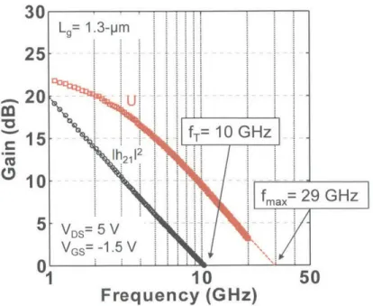
Figure 2-6. DC (a) output and (b) transfer characteristics of AlGaN/GaN HEMT with gate length of 1.3-m . ... 4 0 Figure 2-7. RF measurement setup and flow of the mixed signal. ... 41
Figure 2-8. Layouts for (a) device-under-test, (b) open, and (c) short pattern. ... 42
Figure 2-9. RF characteristics of AlGaN/GaN HEMT with gate length of 1.3-pm. ... 44
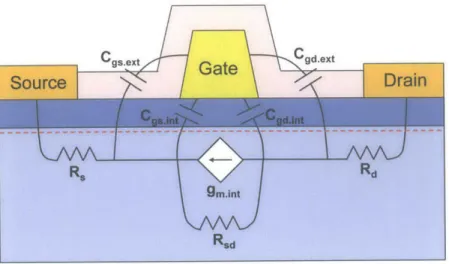
Figure 2-10. A simple small-signal equivalent circuit model for field-effect transistors. ... 45
Figure 3-1. The electron velocity and electric field characteristics of GaN and other semiconductors [7 3 ]. ... 4 8 Figure 3-2. fTs of AlGaN/GaN HEMTs reported in literatures. ... 49
Figure 3-3. Small-signal equivalent circuit model based on the delay analysis method. ... 51
Figure 3-4. (a) T-gate with about 50 nm foot length. (b) Structural instability of T-gate with sub-50 nm foot length. (c) Misalignment between gate head and foot. ... 54
Figure 3-5. Process flows for (a) double layer and (b) single layer electron-beam lithography. ... 55
Figure 3-6. Comparison of DC (a) output and (b) transfer characteristics of AlGaN/GaN HEMTs with gate length of 160 nm and 30 nm . ... 56
Figure 3-7. (a) RF characteristics of 160 nm and 30 nm gate length AlGaN/GaN HEMTs and (b) comparison of the fis of AlGaN/GaN HEMTs with literature data. ... 57
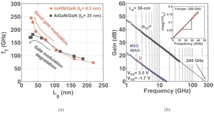
Figure 3-8. fT-Lg product of AlGaN/GaN HEMTs in literatures and this experiment as a function of aspect ratio (L g/tb). ... 5 8
Figure 3-9. (a) Comparison of lattice constant and energy gap between Ino.17A1o.83N and other nitride
alloys [84]. (b) Comparison of simulated 2-DEG sheet charge density between InAlN/GaN and A lG aN /G aN heterostructure [87]. ... 61
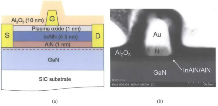
Figure 3-10. (a) Cross-sectional schematic image of InAlN/GaN HEMT. (b) Cross-sectional TEM image of 30 nm gate length device. ... 62
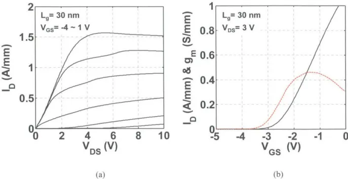
Figure 3-11. DC (a) output and (b) transfer characteristics of 30 nm gate length InAlN/GaN H E M T . ... 6 3
Figure 3-12. Comparison of the subthreshold characteristics of InAlN/GaN and AlGaN/GaN HEMTs. (a) DIBL as a function of gate length. DIBL is extracted in VDS=1 and 5 V at ID=1 mA/mm. (b) Subthreshold characteristics of 30 nm gate length devices at VDS=l and 5 V. ... 64
Figure 3-13. Normalized intrinsic transconductance as a function of the gate length in InAlN/GaN and AlGaN/GaN HEMTs. The inset shows the intrinsic transconductance before normalization. ... 65
Figure 3-14. (a) Maximum fT as a function of the gate length in InAlN/GaN and AlGan/GaN HEMTs. (b) RF characteristics of 30 nm gate length InAlN/GaN HEMT. ... 66
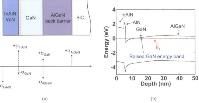
Figure 3-15. Energy band structure of InAiN/GaN HEMT in (a) active and (b) pinch-off regimes. .... 68 Figure 3-16. (a) Polarization charge distribution and (b) energy band structure simulation of InAIN/GaN heterostructure w ith AlGaN back barrier. ... 69
Figure 3-17. Simulation result of the band structure of InAlN/GaN heterostructure with AlGaN back barrier depending on the Aluminum composition. ... 69
Figure 3-18. Cross-sectional schematic images of (a) control InAlN/GaN heterostructure and (b) InAlN/GaN heterostructure with AlGaN back barrier. ... 71
Figure 3-19. Comparison of DC (a) output and (b) transfer characteristics of 65-nm gate length InAIN/GaN HEMTs with and without AlGaN back barrier. ... 72
Figure 3-20. Comparison of subthreshold characteristics of InAIN/GaN HEMTs with and without AlGaN back barrier. (a) DIBL as a function of the gate length. (b) Subthreshold characteristics of 65-nm gate len g th d ev ices. ... 7 3
Figure 3-21. (a) Cross-sectional TEM image of 27 nm gate length device. DC (b) output and (c) transfer characteristics of the device. ... 74 Figure 3-22. Comparison of (a) subthreshold and (b) pinch-off characteristics of the 30-nm gate length range devices with and without back barrier. ... 75
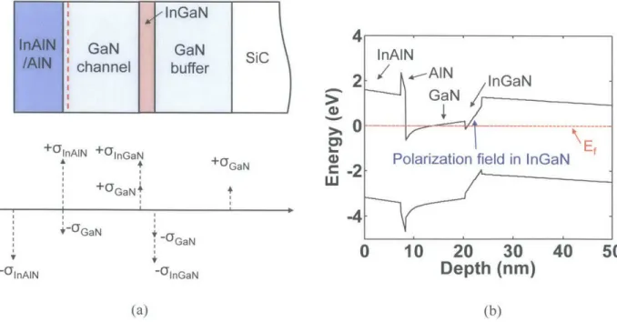
Figure 3-23. RF characteristics of 27 nm gate length InAlN/GaN HEMT with AlGaN back barrier. ... 75 Figure 3-24. (a) Polarization charge distribution and (b) energy band structure of Ino.17Al0.83N/GaN
heterostructure with lno15.Gao8ssN back barrier. ... 76
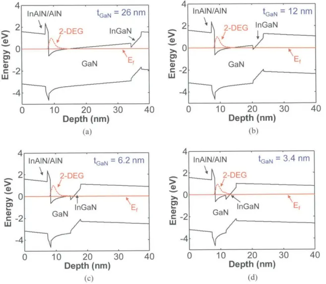
Figure 3-25. Cross-sectional TEM images of heterostructures with (a) 26 nm GaN channel and (b) 3.4 nm G aN ch ann el. ... 7 7 Figure 3-26. Energy band diagram simulation results depending on the GaN channel thickness (a) tGaN=
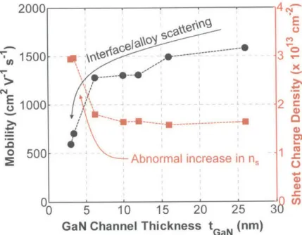
26 nm, (b) tGaN=12 nm, (c) tGaN= 6.2nm, (d) tGaN= 3.4 nm. ... 78 Figure 3-27. Mobility and 2-DEG charge density depending on GaN channel thickness in InAlN/GaN heterostructures. ... 79 Figure 3-28. Contact resistance depending on GaN channel thickness. The inset shows the contact resistance depending on annealing temperature in 3.4 nm GaN channel wafer. ... 80
Figure 3-29. DC transfer and output characteristics of 30-nm gate length InAlN/GaN HEMTs with different GaN channel thickness (tGaN 26, 12, 6.2, 3.4 nm). ... 81 Figure 3-30. (a) DIBL as a function of gate length in the devices with different GaN channel thickness. (DIBL is extracted at ID 10-3 A/mm.) (b) Subthreshold characteristics of 30 nm gate length devices with
different G aN channel thickness. ... 82
Figure 3-31. (a) Leakage current at VGs= -6 V in the devices with different GaN channel thickness. (b) Leakage current path in the devices at pinch-off regime. ... 82
Figure 3-32. (a) Maximum fT as a function of the gate length in the devices with different GaN channel thickness. (b) RF characteristics of 30-nm gate length devices. ... 83
Figure 3-33. Delay analysis process: (a) extraction of the intrinsic and extrinsic capacitances (b) intrinsic transconductance depending on the gate length. ... 85
Figure 3-34. Delay extraction results of the devices with different GaN channel thickness at VDS= 4 V. (a) tGaN 26 nm, (b) tGaN 12 nm, (c) tGaN= 6.2 nm, (d) tGaN 3.4 nm .---...-... 86
Figure 3-35. Average electron velocity and mobility of the devices with different GaN channel thickness. ... . . . ... 87
Figure 4-1. Distribution of each delay component in different gate length devices. ... 90
Figure 4-2. Simple small-signal equivalent circuit model for (a) ideal transistor with no source/drain resistances and infinite output resistance and (b) real transistor with non-zero source/drain resistances and finite output resistance. ... 92 Figure 4-3. (a) Sheet and contact resistances depending on the temperature. (b) On-resistance depending on the tem perature. ... 94 Figure 4-4. DC (a) output and (b) transfer characteristics of 40-nm gate length device at 300 and 77
K . ... 9 5
Figure 4-5. (a) RF characteristic of 40-nm gate length device at 300 and 77 K. (b) fT as a function of the drain bias at different tem peratures. ... 95
Figure 4-6. Schematic image of sub-30 nm device with extremely low on-resistance. ... 98
Figure 4-7. (a) TLM1 pattern and its measurement result. (b) TLM2 pattern and its measurement resu lt. ... 9 9 Figure 4-8. DC characteristics of the devices with gate length of (a) 50-nm and (b) sub-30 nm. ... 100 Figure 4-9. (a) Comparison of the maximum fT between devices in this experiment and devices used in section 3.5.3. (b) RF characteristic of sub-30 nm gate length device. ... 101
Figure 4-10. (a) Delay analysis result of devices with regrowth contact and scaled source/drain distance
(LSD). (b) Comparison of delay analysis of 30-nm gate length devices with Ron > 1 2-mm (alloy contact
and LsD> 1 [tm) and Ron < 0.5 £-mm (regrowth contact and LSD <0.7 gm). ... 102
Figure 4-11. Parasitic delay components depending on the gate length. ... 103
Figure 4-12. Cross-sectional device structure used in this study. ... 105
Figure 4-13. DC (a) output and (b) transfer characteristics of sub-30nm gate length devices with A1203
passivation thickness of 10 nm and 40 nm . ... 106 Figure 4-14. DIBL in the devices with the passivation thickness of 10 nm and 40 nm. ... 106 Figure 4-15. Current collapse depending on the passivation thickness and comparison of the DC and pulsed-IV characteristics of the devices with passivation thickness of 10 nm and 40 nm. ... 107 Figure 4-16. (a) fT as a function of the gate length depending on the passivation thickness (tpass). (b)
Degradation of fT with increasing the passivation thickness. (c) Cross-sectional image of the gate fringing capacitance due to increase of the passivation thickness. ... 108
Figure 4-17. Extracted Cgs and Cgd in (a) saturation bias condition (VDS= 3 V, VGS -3.5 V) and (b)
ON-state condition (V DS= 0 V , V GS= OV ). ... 110
Figure 4-18. Gate capacitance distribution at the pinch-off bias condition. ... 110
Figure 4-19. Extraction of the gate fringing capacitance at the pinch-off condition. ... 111
Figure 4-20. Gate capacitances extracted from the simulation results from different gate length. ... 112
Figure 4-21. Gate fringing capacitance extraction from the simulated gate capacitance at (a) pinch-off condition and (b) O N -state condition. ... 113
Figure 4-22. Gate fringing capacitance extracted from the measurement depending on the passivation th ick n ess. ... 1 14 Figure 4-23. (a) Simulation device structure for T-gate and (b) gate fringing capacitance depending on passivation thickness and T-gate height. ... 115
Figure 4-24. (a) Gate capacitance modeling. (b) Intrinsic transconductance model including short channel effect. (c) Output resistance model including short channel effect. ... 116
Figure 4-25. fT projection depending on the technology improvement. ... 116
Figure 4-26. RF characteristics of sub-30 nm gate length device. ... 117
Figure 5-1. fT as function of VDS in different gate length devices. ... 121
Figure 5-2. N. Moll delay time analysis method [40]. Extraction methods of (a) channel charging delay and (b) drain delay . ... 122
Figure 5-3. Cross-sectional image of GaN device under deep saturation regime. ... 124
Figure 5-4. (a) Lateral electric field and (b) electron charge distribution in the depletion region based on the charge control model used for base-collector junction in BJT. (This model can be used for drain-side depletion region in H EM T .) ... 125
Figure 5-5. Small-signal equivalent circuit model including the gate extension effect. ... 127
Figure 5-6. Change of each delay component with increasing drain voltage. (a) 1, (b) T2, (c)T3. .... . . . . .128
Figure 5-7. Drain delay extracted from 220-nm gate length device based on the different extraction m eth o d . ... 13 0 Figure 5-8. Drain delay extracted from the short channel devices. (a) Lg=120-nm, (b) Lg=60-nm. ... 131
Figure 5-9. Change of (a) Cgs and (b) gmint with increasing drain voltage in different gate length d ev ices. ... 13 2 Figure 5-10. Change of DC gmwith drain voltage. (a) Lg=40-nm, (b) Lg=60-nm, (c) Lg=330-nm...1 33 Figure 5-11. Extracted drain delay rate as a function of the gate length. The drain delay rate increases rapidly as the gate length scales down below about 100 nm. ... 134
Figure 5-12. (a) Blocking the path of punch-through current with structure of vertical channel scaling. (b) Comparison of the gm.int degradation at high drain bias between the devices with vertical GaN channel scaling and control structure. ... . -... -.. ... 135
Figure 5-13. Comparison of the drain delay rates in the 80-nm gate length devices with vertical GaN channel scaling and control structure. ... 136 Figure 5-14. (a) Schematic and top view SEM image of the device with scaled gate-to-drain spacing. (b) Comparison of the fT trends at high drain bias between devices with Lgd= 100-nm and Lgd=
350-n m . ... ... 13 9
Figure 5-15. (a) Expansion of the depletion region width and (b) change of Cgd in the devices with Lgd= 100 nm and 300 nm . ... 140 Figure 6-1. Nonlinearity of (a) g. and (b) fT in GaN HEMTs with different gate length. ... 142 Figure 6-2. Two different explanations about origin of gm nonlinearity. (a) Non-linear source access resistance [139]. (b) Optical phonon scattering [143]. ... 144
Figure 6-3. (a) Device structure of self-aligned GaN HEMTs and DC (b) output and (c) transfer characteristics of the device [127]. ... 145 Figure 6-4. (a) Cross-section schematic of short channel GaN device under saturation. (b) Simulation of longitudinal electric field and resistance in the source access region [139]. (c) Electron velocity depending on electric field in the different transport model [139]. ... 147
Figure 6-5. Device structure of the nanowire channel GaN HEMT. ... 148
Figure 6-6. Previous studies about nanowire channel GaN devices. (a) [145], (b) [146], (c) [162]. ... 149 Figure 6-7. Fabrication process of the nanowire channel GaN HEMT. (a) Mesa isolation and ohmic contact formation, (b) Si3N4 deposition and nanowire patterning with e-beam lithography and selective dry etching with CF4 plasma, (c) gate e-beam patterning with ZEP520 resist, (d) top barrier and GaN
channel dry etching with BCl3/Cl2 plasma, (e) Si3N4 pattern removal with dry etching with CF4 plasma,
(f) gate metal deposition and lift off, (g) removal of Si3N4 pattern on the access region with BOE wet etching, (h) A1203 passivation layer deposition with ALD. ... 150
Figure 6-8. Top view SEM image of (a) Si3N4 nanowire pattern and (b) device after gate lift off process.
Only under the gate, the channel is etched. ... 151
Figure 6-9. (a) SEM and (b) AFM images of the test structure after removing gate metal. ... 151
Figure 6-10. DC (a) transfer and (b) output characteristics of 70-80 nm gate length nanowire channel device and conventional planar device. The nanowire channel device characteristics are normalized based on the effective channel w idth. ... 153 Figure 6-11. (a) Gate current injection method and (b) source resistance extracted by the method. ... 154
Figure 6-12. DC (a) transfer and (b) output characteristics of nanowire channel device and conventional
device based on the entire device width normalization. ... 155
Figure 6-13. (a) Variation of nanowire channel width in the device layout. (b) Extrinsic gm as a function of the gate voltage in the devices with different width ratio. ... 156
Figure 6-14. Test device structure to study the effect of the nanowire width. ... 157
Figure 6-15. DC (a) transfer and (b) output characteristics of the test structure and planar device. ... 158
Figure 6-16. Current flow in (a) nanowire device and (b) test structure with wide channel width. ... 158
Figure 6-17. Test device structure to study the surrounding gate effect. ... 159
Figure 6-18. DC (a) transfer and (b) output characteristics of the test structure and conventional planar dev ice. ... ... 15 9 Figure 6-19. f1 as a function of the gate voltage in the nanowire channel device and conventional planar dev ice. ... ... . . . ... 16 0 Figure 6-20. Fringing capacitances in the nanowire channel device. (a) Fringing capacitance between gate and sidewall of the nanowire. (b) Fringing gate capacitance between gate and additional access reg io n . ... 16 1 Figure 7-1. (a) Improvement in fT of deeply-scaled GaN HEMTs through this work. (b) Comparison of the fTs in this work with those of AlGaN/GaN HEMTs reported in the literature (Figure 3-2). ... 167
List of Tables
Chapter 1. Introduction
1.1. Nitride-based semiconductors
In recent 20-30 years, a nitride-based semiconductor technology has been tremendously developed since critical issues hindering its progress, such as high quality growth and p-type doping, have been solved through extensive research [1], [2]. The outstanding material properties of the nitride alloys have stimulated many different fields, which expands many possible application areas as shown in Figure 1-1.
In optoelectronics, the wide range of potential energy band gaps from 0.7 eV (InN) to 6.2 eV (AlN) can provide a single complete solution for emission and detection from infrared to ultraviolet. Since the first GaN electroluminescent diode was demonstrated in 1971 [3], a light emitting diode (LED) technology based on the nitride alloys has been improved remarkably [2],
IRF
(Wireless Base Stations)Power Transistors
MEMS (Pressure Sensors)\ Switches (Display Panels) Engine Electronics (Temperature Sensors)
High Frequency MMICs (Wireless Broadband)
Power Conversion (Automobiles / Aircrafts)
Solid State Lighting White/Blue/UV LEDs)
UV Detectors (Bio Detection)
Blue Laser Diodes (DVD Storage)
Hydrogen Generation (Fuel Cells)
[4] and the first commercial nitride-based LEDs were launched in Nichia Chemical Industries in 1993. Also, the potential optoelectronic applications have expanded from the original LEDs, to photo detector [5] and laser diodes [6].
In addition, the high structural stability and Young's modulus, as well as strong piezoelectricity of these materials make them attractive for microelectromechanical systems (MEMS). For example, GaN cantilevers [7], [8] and surface acoustic wave (SAW) devices [9], [10] were demonstrated by using these excellent properties. In addition, chemical and biological applications such as gas sensor and bio sensor were explored [11], [12].
In electronics, GaN-based devices are a very promising candidate for both high power and high frequency applications. Table 1-1 shows a comparison of key electrical properties of various semiconductors. Compared to other semiconductors such as Si and GaAs, GaN can provide a significantly larger breakdown voltage for a given on resistance thanks to its high critical electric field. Moreover, high electron mobility and saturation velocity allow GaN-based devices to operate at very high frequencies. SiC has many properties similar to GaN, but several critical issues such as challenge in heterostructure design and extreme process condition limit its applications. In contrast, GaN can form heterojunctions with other nitride alloys and this makes
Semiconductors GaAs InP sic GaN
Properties Unit (AIGaAs/InGaAs) (InAIAs/InGaAs) (AIGaN/GaN)
Band gap eV 1.11 1.42 1.35 3.26 3.39 Critical MV/cm 0.3 0.4 0.5 3 3.3 breakdown field Saturated (peak) x 107 cm/s 1.0 1.3 1.0 2.0 1.3 electron velocity (1.0) (2.1) (2.3) (2.0) (2.5) Electron mobility cm2/V-s 1350 8500 5400 700 2000 at 300 K
it possible to utilize high-electron mobility transistor (HEMT) structure which has been widely used in many other semiconductor systems. Moreover, a two-dimension electron gas (2-DEG) induced by the polarization effect in the heterojunctions makes device fabrication simple, removing need for additional doping process. Based on these advantages, GaN electronics has been developed significantly in the past three decades.
1.2. GaN transistors
The first demonstration of GaN-based transistors was based on MESFET structure [13]. However, after the existence of the 2-DEG with high mobility was verified in AlGaN/GaN heterostructures [14]-[16], the HEMT structure has become the main device structure for GaN transistors [17]. The potential of GaN transistors which can provide both large breakdown voltage and high speed operation has attracted two main commercial areas: 1) power switching and 2) RF high power amplification, as shown in Figure 1-2. Although there is no fundamental difference in the basic device structure, the device design and target performance vary depending on the specific application.
(a) (b)
1000
GaN (MIT 2011) Si Limit GaN (IR)
I GaN (EPC)
0 GaN (other research labs)
E 100 0 Sic Si Super-Junction 1 Si IGBT U) 0 10. .... - - -- - --- -... 10 10O
Uk
(A Sic Limit GaN Limit
0.11
100 1000 10000
Breakdown Voltage (V)
Figure 1-3. On-resistance and breakdown voltage in different semiconductor device technologies
In the case of devices for power switching, their operating frequency range is typically below GHz (kHz - MHz), while the breakdown voltages vary from a few tens of volts to a few thousands of volts. In addition to the breakdown voltage, the device on-resistance is another important parameter, which is critical to maximize the energy efficiency of power electronics circuits. Thus, the product of the breakdown voltage and specific on-resistance is one of the most important figure-of-merits (FOMs) in this application. Figure 1-3 shows theoretical comparison and experimental results of the FOM of GaN transistors with other semiconductor technologies. The theoretical estimation based on the material parameters anticipates more than an order-of-the-magnitude better performance in GaN transistors than conventional Si devices. Also, research GaN transistors already outperform commercial Si devices optimized for best performance. Although there are still many issues which need to be solved for successful commercialization, these results clearly show the huge potential of GaN devices in power electronics.
100 0) C 0 C 0
ma
10 1 10 100fT
[GHz]
1000Figure 1-4. Breakdown voltage and current gain cutoff frequency (fT) of different semiconductor devices (modified from [18]). GaN device has a potential to outperform other devices thanks to its outstanding material properties.
Another promising application for GaN transistors is in RF power amplifiers. In the devices
targeting this application, maximum output power and operating frequency are the most
important parameters. As these two parameters are closely related to the breakdown voltage and
electron velocity, GaN is an ideal candidate to improve the performance of the RF power
amplifiers to the next level as shown in Figure 1-4 [18]. Since the first microwave characteristics
of AlGaN/GaN HEMT were reported in 1994 [19], there have been extensive efforts to improve
its performance. Specifically, the research on RF devices has focused on two topics: 1)
large-signal power performance, 2) small-large-signal frequency characteristics.
The large-signal power performance including maximum output power density (Put) and
power-added efficiency (PAE) is closely related to the required specs of power amplifiers. These
* Si BJT ANTT GaN HFET
4A A MIT
SInPH8T GaNHFETA C GaNHFET
A HFET
A GaN HFET A UCSO
SSi NMOS A GaH HFET HIRL A MP DHBT TRW - 'l xdAkaWn DHBT P SHBT WVesse % S NEC T HflW DHBT *kIPDHBT IM IBM SIGe h BJT leomWs Sim Si BJT Hitachi-SiGo HBT -
Dahniea-Benz-SiGe HBT IBM SIGe 9HP 9HP
characteristics are measured at a target operating frequency and show how much power can be delivered efficiently from the devices. The first large-signal RF characteristics were measured with 1 -tm gate length AlGaN/GaN HEMT at 2 GHz in 1996 [20]. The device showed Po0 t of 1.1 W/mm and PAE of 18.6 %. Since then, both the operating frequency and power performance have been increased significantly. Wu et al. reported P0ut of 3.3 W/mm and PAE of 18.2 % at 18
GHz in 1997 [21] and Moon et al. demonstrated a 0.15 tm gate length device with Po0t of 6.6
W/mm and PAE of 35 % at 20 GHz [22]. In 2004, by using a field-plate technology [23], Chini
et al. demonstrated devices with Pout of 12 W/mm and PAE of 58 % at 4 GHz [24] and Wu et al.
significantly improved P0ut to 41.4 W/mm with PAE of 60 % at the same frequency [25]. In 2005,
Palacios et al. reported P0ut of 10.5 W/mm and PAE of 33 % at 40 GHz [26] and Wu et al.
improved Po0t to 13.7 W/mm and PAE to 40 % at 30 GHz in 2007. In addition, many promising
results in high frequency band such as V and W bands have also been reported [27]-[29].
Complementary to the large-signal power performance, the small-signal characteristics highlight the potential of devices by providing information about their maximum possible operating frequency. Current gain cutoff frequency (fT) and power gain cutoff frequency (fmax) are the most important figure of merits (FOMs) in the small-signal performance. Since the possible operating frequency range of a real application is determined based on these metrics, improving the cutoff frequencies is an important step to expand the potential application area. Since Khan et al. reported the first small-signal microwave characteristics of 0.25-[tm gate length AlGaN/GaN HEMT with fT= 11 GHz and fmax= 35 GHz [19], there has been a continuous increase of both fT and fmax as shown in Figure 1-5. Khan et al. increased the maximum fT and
fmaxto 36.1 GHz and 70.8 GHz, respectively in 0.25-tm gate length device in 1996 [30]. Wu et al. demonstrated fT of 50 GHz and fmax of 92 GHz in the device with a gate length of 0.2 pim in
400
AIGaN/GaN HEMTs [38] fmax 300 - -N [37] [35] T in ,[39] M 200 [34], E *[37] [33] "*W [36] I [32] [34] 100 . .32] [30] ,/ [31] [19] [31 [19]' [30] 190 1995 2000 2005 2010 2015 YearFigure 1-5. Evolution of fT and fmax in AlGaN/GaN HEMTs. Highest frs and fmaxs reported in each year (1994-20 10) were plotted in this figure.
1997 [31] and Micovic et al. improved the f1 to 110 GHz and fmax to 140 GHz with 0.15 ptm gate
length device in 2000 [32]. In 2002, Kumar et al. fabricated 0.12 m gate length device with f1 of 121 GHz and fmax of 162 GHz [33]. In 2005, Palacios et al. demonstrated 90 nm gate length
device with fT of 163 GHz and fmax of 185 GHz [34]. In 2006, Palacios et al. pushed the fmax to 230 GHz by using InGaN back barrier structure in 100 nm gate length device [35] and Higashiwaki et al. improved the f1 to 181 GHz by scaling the gate length to 30 nm [36]. In 2008,
with 60 nm gate length AlGaN/GaN HEMT with thin barrier, Higashiwaki et al. reported fl of
190 GHz and fmax of 251 GHz [37]. Finally, in 2010, Chung et al. obtained a new record performance, f- of 225 GHz and fmax of 300 GHz in the 55 nm and 60 nm recessed-gate
200 S150 9100 fT drop in high VDS 200 Low maxim 50 150 kL g 0-n .100 -3 50 ~20 L =3O-nm 1VDS=3 00 2 4 6 8 10 VGS= -5.6V VDs (V) 010 t\~NFrequency urn fT (GHz 200 fT dirop in high VGS
4
-4 VGS (V) VDs (V) 2 0 -10 -8 VGS (V)Figure 1-6. fT distribution of 30-nm gate length AlGaN/GaN HEMTs. The plot shows the critical issues in the device speed of the deeply-scaled GaN HEMTs: (1) low maximum fT, (2 fr roll-off at high drain and gate bias ranges.
1.3.
Issues in GaN RF devices
In spite of the significant improvement in microwave performance of GaN HEMTs, there are still many unsolved problems. Especially, two critical issues related to the speed of the devices are summarized as shown in Figure 1-6.
1.3.1. Low maximum device speed
As mentioned in the previous section, the device speed or current gain cutoff frequency (f1) of
GaN HEMTs has been increased continuously. The main strategy to increase the speed of the L g= 30-nm
device has been gate length scaling and the minimum gate length has been dramatically decreased to about 30 nm range [36]. However, in spite of the extremely scaled gate length, the maximum device speed is much lower than both the theoretical expectations based on the material properties and projections based on experimental long channel devices. Moreover, the variation of the device speed depending on the technology becomes larger in shorter channel devices. In order to realize the potential of GaN transistors, the causes for degradation and variation of the speed in the deeply-scaled devices need to be clarified. Also, new technologies to overcome these challenges are necessary.
1.3.2. Roll-off of the device frequency performance at high biases
Compared to other high frequency semiconductor devices based on GaAs or InP, one of the main differences in GaN RF devices is the large signal operation required to delivered high output power. In order to support high speed large-signal operation, maintaining high frequency performance over a wide bias range is as important as pushing the maximum speed at a given bias condition. However, as shown in Figure 1-6, the speed of a typical GaN device decreases rapidly with increasing both drain bias and gate bias. Moreover, it is observed that the degradation becomes more significant in shorter gate length devices, which makes it one of the key challenges in the deeply-scaled GaN HEMTs. The decrease in device speed at high drain bias has been already studied in other semiconductor devices and the effect, which is called drain delay, has been measured based on the method proposed by Moll et al.[40]. However, it is challenging to understand the essence of the effect accurately since the extraction method is not based on theoretical and mathematical background. In the case of the decrease of the device speed at high gate bias or high drain current, its origin has been controversial. Since there is no
solid understanding about these problems, it is very challenging to find a good solution to overcome them.
1.4. Project goal and thesis outline
This thesis addresses two key issues regarding the speed of the deeply-scaled GaN HEMTs, described in the previous section. First, in order to identify what limits the maximum speed of these devices, systematic analysis of the device speed is performed by revisiting the device physics. Based on the study, new technologies are applied to overcome these challenges and push the device speed to the next level. Then, the origin of the roll-off of the device speed in the wide bias range is investigated through both theoretical and experimental studies. Based on the analysis, new approaches to minimize the effects are developed.
The thesis is organized as follows:
In chapter 2, the basics of GaN HEMT technology are concisely outlined. The mechanism of GaN heterostructures and device fabrication process are described. In addition, both DC and RF characteristics of typical GaN HEMTs are explained, highlighting important figures-of-merits.
In chapters 3 and 4, the limitation in the maximum speed of the deeply-scaled GaN HEMTs is studied in detail by dividing the device into intrinsic and extrinsic regions. In chapter 3, the limiting factors in the intrinsic device performance are described. In order to suppress the increase of the intrinsic delay caused by the degradation of the gate modulation efficiency, an InAlN/GaN heterostructure is applied to a 30 nm gate length device, which allows a maximum f1 of 245 GHz, higher than any other GaN HEMTs demonstrated previously. In addition, to
improve the subthreshold and pinch off characteristics, two different approaches are investigated. Both AlGaN back barrier structure and vertical channel scaling technologies contribute to the improvement of the device performance by increasing the channel charge confinement. Also, the relevant trade-offs of each technology are also discussed for further optimization. Thanks to these studies, the maximum speed of GaN HEMTs is pushed to 300 GHz.
Chapter 4 studies the extrinsic device components limiting the maximum device. First, the effect of the parasitic resistances is investigated through characterization at low temperature. To reduce these parasitic resistances, several technologies including heterostructure with low sheet resistance, sub-[ m source-to-drain distance, and regrowth contact have been combined in this work and the total device resistance is decreased to about 0.4 Q-mm. As the second extrinsic device component, the impact of the fringing gate capacitance is investigated, focusing on the passivation layer. The significant influence of the fringing gate capacitance on the speed of deeply-scaled devices is studied based on both experimental results and device simulation. Based on these studies, we show that maximum device speed over 400 GHz is possible in the 30 nm gate length range. An experimental device with a maximum fT of 375 GHz is demonstrated by minimizing the extrinsic components.
In chapter 5 and 6, the roll-off of the device frequency performance at high biases is discussed. In chapter 5, in order to study the drain delay more accurately, a new extraction method is proposed based on the small-signal equivalent circuit model and it is compared to the other methods in literature. In addition, based on the proposed method, it is shown that rapid decrease in the speed of short channel devices at high drain bias is not only caused by the drain delay
effect, but also degradation of the gate electrostatics. In order to reduce the delay resulting from these effects, technologies with vertical channel scaling and lateral gate-to-drain distance scaling are investigated.
In chapter 6, the origin of the decrease of device speed with increasing gate bias (or drain current) is identified. In order to prove that it results from the limitation of the current supply in the source access region, a novel nanowire channel structure with sub-100 nm gate length is developed. The proposed nanowire channel device solves the nonlinearity of gm and fT thanks to its higher current drivability of the source access region compared to that of the intrinsic channel. Moreover, the current density of the nanowire channel is increased over 3 A/mm which is closer to the theoretical expectation. These results do not only verify that drop of the device speed at high gate bias is caused by extrinsic source region, but also emphasize the importance of the source design to realize the full potential of intrinsic GaN HEMTs.
Finally, chapter 7 summarizes the main results of this thesis. In addition, future research directions are proposed to further improve the speed of the deeply-scaled GaN HEMTs.
Chapter 2. Basic Device Design and Physics in GaN HEMTs
In this chapter, the basic device design and physics parameters in GaN-based high electron mobility transistors (HEMTs) are briefly explained, including polarization, device fabrication process, and DC/RF characteristics.
2.1. Polarization in GaN-based heterostructures
The most common crystalline structure in GaN is wurtzite, with Gallium (Ga) and Nitrogen (N) atoms ionically bonded. Due to the difference in the electron affinity between two materials, the distribution of valence electrons in the bonding becomes strongly asymmetric, which combined with the lack of center symmetry in the wurtzite structure induces a polarization field. In other compound semiconductors such as GaAs and InP, the polarization field also exists in each ionic bonding through the same mechanism, but it is almost cancelled out because of the symmetry of their zincblende crystal structure (Figure 2-1(a)) and the net polarization becomes close to zero.
(a) (b)
Ga-face N-facm
Ga N
N Ga
Substrate Substrate
(a) (b)
Figure 2-2. Crystal structure and polarization field in (a) Ga-face and (b) N-face GaN [41].
In GaN, however, wurtzite crystal structure prevents the offset and generates a fairly large net
polarization field in the c-axis direction (Figure 2-1(b)). Depending on the growth direction, GaN can be divided into Ga-face and N-face, and the direction of the polarization field becomes opposite as shown in Figure 2-2 [41]. (Research in this thesis is based on Ga-face structure and the following also assumes the Ga-face unless mentioned otherwise.) This polarization field is an intrinsic material property determined by chemical elements and crystal structure, so that it is called as a spontaneous polarization (Psp).
In GaN heterostructures such as AlGaN/GaN, InAlN/GaN, and AlN/GaN, there is an additional polarization component in addition to the spontaneous polarization. Once the top layer (AlGaN, InAlN, or AlN) is grown on top of the GaN, it gets strained due to the lattice mismatch. If the layer thickness is below its critical thickness, the strain is maintained and it induces piezoelectric
polarization (PPZ) [14]. Thus, the polarization in the heterostructure is typically combination of
GaN Substrate a2 2D - EG
E-- -- --
--+UAIGaN GaN Substrate
+CJGaN 4, 0 GaN 0 AIGaN (a) (b)
Figure 2-3. (a) Polarization charge distribution of AlGaN/GaN heterostructure. (b) 2-DEG induced by
polarization field.
with a polarization charge at the interface and Figure 2-3(a) shows the polarization charge distribution in AlGaN/GaN heterostructures.
Large energy band bending caused by high polarization field in the top barrier layer generates donor-like surface states and free electrons. As shown in Figure 2-3(b), the free electrons slide down to GaN, following the electric field and accumulate at the interface between the top barrier layer and the GaN, forming a two dimensional electron gas (2-DEG) [42]. This process continues until the Fermi level is pinned at the ionized donor-like surface state level. Thanks to the sharp interface at the heterostructure and the separation from the positive charges of the surface states, the 2-DEG can have a high mobility over 1000-2000 cm2-V/s [43], [44]. Also, the high
polarization field in the structure allows the density of the 2-DEG to go over 1013 cm~2. The combination of high mobility and large charge density, which is unique compared to other semiconductors, makes GaN a very promising candidate for high frequency and high power applications.
2.2. Fabrication process of GaN HEMTs
Compared to Si MOSFETs, the fabrication process of conventional AlGaN/GaN HEMTs is significantly simpler. The 2-DEG channel, which is formed spontaneously at the heterostructure interface, eliminates the need of any additional doping process such as implantation and dopant activation annealing. In addition, since the top AlGaN layer isolates the gate electrode from the channel thanks to its larger band gap and high Schottky barrier, a gate oxide formation step similar to the one in Si MOSFET technology is not required.
Figure 2-4(a) shows an example of an initial AlGaN/GaN wafer structure. As a substrate for the GaN growth, Si, sapphire or SiC is widely used. On top of the 1-2 tm GaN, AlN interlayer and AlGaN top barrier are grown pseudomorphically to form heterojunction. The AlN interlayer is typically inserted between top barrier (AlGaN) and GaN in order to improve the 2-DEG mobility by reducing alloy disorder scattering [45]. Figure 2-4(b)-(f) shows an example of conventional fabrication process of AlGaN/GaN HEMTs. The process begins with mesa isolation with BCl2/C12-based plasma dry etching as shown in Figure 2-4(b). The depth of the mesa etching
(150 ~ 200 nm) should be much deeper than that of the 2-DEG channel to reach complete
isolation. The sidewall of the mesa is depleted due to the plasma damage and Fermi level pinning at the surface, which prevents the leakage current through the sidewall contact. As an alternative method for device isolation, implantation is also widely used [46]-[49]. The damage induced by the implantation destroys the 2-DEG channel outside the active area, which provides isolation effect. Compared to the mesa isolation, the advantage of the implantation isolation is that it does not generate a large step height, which is favorable for subsequent technology processes.
After device isolation, source/drain contacts are made through photo lithography and subsequent metal stack deposition as shown in Figure 2-4(c). In the conventional contact process,
I imtin )AIN AIN
GaN (1 ~ 2 pm) GaN - GaN
Substrate (SiC, A1203, Si) Substrate Substrate
(a) (b)
(c)
AIGaN A NAfftN
AIN AIN AIN
GaN ~- ~-GaN GaN
Substrate Substrate Substrate
(d) (e) (
Figure 2-4. Fabrication process of GaN HEMTs. (a) Wafer preparation, (b) mesa isolation, (c) ohmic contact metal deposition, (d) metal annealing, (e) gate metal deposition, (f) passivation layer deposition.
a Ti/Al-based metal stack is widely used such as Ti/Al/Ni/Au [50], Ti/Al/Mo/Au [51], and Ti/Al/Ti/Au [52]. After the deposition, the metal stack forms the Schottky contact to the AlGaN top barrier. To make it an ohmic contact, a high temperature annealing above 700-800 'C is required as shown in Figure 2-4(d). Depending on the heterostructure, the optimum annealing condition varies, but generally, it is between 800 'C and 900 'C. During the high temperature annealing, Ti forms TiN with AlGaN layer introducing N-vacancies near the interface, which act as donor states, creating a tunnel junction to reduce the contact resistance [53], [54]. The combination of TiN, n-type doped AlGaN interface, and Ti/Al alloy provide an ohmic contact in the heterostructure. The top Ni/Au layers prevent the oxidation of Ti/Al and Ni also acts as a diffusion barrier for Au into Al. After annealing of the metal stack, the surface of the contact
becomes rough due to the alloy of the different metal layers. The contact resistance in the conventional alloy contact process described above is about 0.3-0.6 Q-mm in AlGaN/GaN heterostructure.
After ohmic contact process, a gate electrode is formed between source and drain contacts through gate photo lithography and metal deposition as shown in Figure 2-4(e). Ni/Au or Pt/Au stacks are generally used as gate metal due to the high Schottky barrier height between Ni or Pt and the AlGaN layer. Au is used on top to lower the sheet resistance of the metal stack. Since the gate electrode is defined through a different lithography than the ohmic contacts, there is a space between the gate electrode and the source/drain metal contacts, the access region. In the conventional GaN HEMT process, it is challenging to make a self-aligned device with no access region because of the high temperature annealing needed for ohmic contact formation and the subsequent rough morphology of the annealed contact.
As a final step in the fabrication, a passivation layer is deposited on top of the device to reduce surface trapping and current collapse, as shown in Figure 2-4(f). Several dielectric materials have been used as passivation, including Si3N4 [55], SiO2 [56], and A1203 [57]. Figure 2-5 shows a top
view Scanning Electron Microscopy (SEM) image of the fabricated AlGaN/GaN HEMT.
Figure 2-5. Top view SEM image of the fabricated AlGaN/GaN HIEMT with gate length of 1.3-pm and gate-to-source distance of 5 pm.
Lg= 1.3-pm Lg= 1.3-pm 0.8 VGS -4 V E 0.8 VDS= 1, 3, 5 V
E
0.4- 00 0.4 0 0-0 -- ---- ---0 2 4 6 8 10 5 -4 -3 -2 -1 0 1V
DS (V) VGS (V) (a) (b)Figure 2-6. DC (a) output and (b) transfer characteristics of AlGaN/GaN HEMT with gate length of 1.3-pm.
2.3 DC characteristics of GaN HEMTs
Figure 2-6(a) shows the DC output characteristic of a conventional AlGaN/GaN HEMT with gate length of 1.3 pm. At low drain voltage (VDs), drain current is linearly dependent on VDS and the slope, which is called as on-resistance (Ron), is determined by sum of the contact resistance, access resistance and channel resistance. At high VDS above knee voltage, drain current is saturated and it is mainly determined by gate voltage (VGS). In spite of the long gate length, the maximum drain current of the device is over 0.7 A/mm at a gate voltage (VGS) Of 1 V. (The maximum positive gate voltage (1 -2 V) is limited by the turn-on voltage of the gate Schottky
contact.) As the maximum drain current is determined by the sheet charge density of the heterostructure and electron velocity dependent on lateral electrical field, it can be further increased by using heterostructure with higher polarization charges and scaling the device laterally.
As shown in Figure 2-6(b), the threshold voltage (VT) is typically negative because the polarization-induced 2-DEG channel needs to be depleted to turn off the device (depletion-mode). In order to achieve enhancement-mode operation, additional process or change of heterostructure design is necessary such as gate recess [58], [59], fluorine treatment [60] and InGaN cap layer
[61]. A transconductance (gm), defined as a ratio of drain current change to gate voltage change, is also the important parameter in the transfer characteristic. It typically increases with increasing Vcs and reaches its maximum point at 30-50 % of maximum drain current level as shown in Figure 2-6(b). The gm can be improved by increasing coupling between gate and 2-DEG charges and electron velocity in the channel.
2.4 RF characteristics of GaN HEMTs
The high frequency performance of GaN transistors is typically measured by using a
Vector-Vector Network Analyzer
Bias Tee CBias Tee
[DC Power Supply
Device under Test
Network-Analyzer (VNA) and Figure 2-7 shows a general setup for RF measurement. Before the device characterization, the system is calibrated with standard methods such as Short-Open-Load-Through (SOLT) or Line-Reflect-Match (LRM) to move the reference plane to the end of the probes. High frequency small signal from VNA is combined with DC bias generated by a power supply in a bias tee and the mixed signal is applied to a device-under-test (DUT). Based on the information about input and output signal from the device, S-parameters of the DUT are defined at each bias and frequency. As the conventional transistor can be modeled as a two-port network, a 2 x 2 S-parameter matrix can be obtained from the measurement. A typical device layout has a large pad area for probe contact as shown in Figure 2-8(a), so that the measured S-parameters include the effects of the pad parasitic capacitance, resistance and inductance. A procedure to remove these effects from the measured data is called as de-embedding. In general, the difference before and after de-embedding is minimal in long channel devices due to the large gate capacitance compared to the pad capacitance. However, in the short channel devices, the
S S S
D G D
S S S
(a) (b) (c)