HAL Id: tel-01725224
https://tel.archives-ouvertes.fr/tel-01725224
Submitted on 7 Mar 2018
HAL is a multi-disciplinary open access
archive for the deposit and dissemination of sci-entific research documents, whether they are pub-lished or not. The documents may come from teaching and research institutions in France or abroad, or from public or private research centers.
L’archive ouverte pluridisciplinaire HAL, est destinée au dépôt et à la diffusion de documents scientifiques de niveau recherche, publiés ou non, émanant des établissements d’enseignement et de recherche français ou étrangers, des laboratoires publics ou privés.
Hybrid Metrology Applied to dimensional Control in
Lithography
Nivea Griesbach Schuch
To cite this version:
Nivea Griesbach Schuch. Hybrid Metrology Applied to dimensional Control in Lithography. Mi-cro and nanotechnologies/MiMi-croelectronics. Université Grenoble Alpes, 2017. English. �NNT : 2017GREAT063�. �tel-01725224�
THÈSE
Pour obtenir le grade de
DOCTEUR DE LA
COMMUNAUTÉ UNIVERSITÉ GRENOBLE ALPES
Spécialité : NANO ELECTRONIQUE ET NANO TECHNOLOGIES
Arrêté ministériel : 25 mai 2016
Présentée par
Nivea GRIESBACH SCHUCH
Thèse dirigée par Maxime BESACIER, Maître de Conférence, UGA et codirigée par Jérôme HAZART, Ingénieur de Recherche, Laboratoire d'électronique et de technologie de l'information
préparée au sein du Laboratoire des Technologies de la
Microélectronique et du Laboratoire d’Électronique et de Technologies de l’Information
dans l'École Doctorale Electronique, Electrotechnique,
Automatique et Traitement du Signal (EEATS)
Métrologie Hybride pour le contrôle
dimensionnel en lithographie
Hybrid Metrology applied to
dimensional control in lithography
Thèse soutenue publiquement le 27 octobre 2017, devant le jury composé de :
Madame Jumana BOUSSEY
Directeur de Recherche, CNRS Délégation Alpes, Président
Monsieur Gaoliang DAI
Ingénieur de Recherche, Physikalisch Technische Bundesanstalt - Allemagne, Rapporteur
Madame Tatiana NOVIKOVA
Ingénieur de Recherche, CNRS Délégation Ile de France Sud, Rapporteur
Madame Alexandra DELVALLEE
Ingénieur de Recherche, Laboratoire National de métrologie et d'Essais, Examinateur
Monsieur Patrick SCHIAVONE
Directeur de Recherche, CNRS Délégation Alpes, Président
Monsieur Gérard GRANET
Professeur, Université Clermond-Ferrand 2, Examinateur
Monsieur Maxime BESACIER
Maître de Conférence, UGA, Membre invité
Monsieur Jérôme HAZART
Ingénieur de Recherche, Leti, Membre invité
Monsieur Matthew SENDELBACH
3
This thesis is dedicated to the memory of my mother Enidia Griesbach Schuch, a great mother and wonderful woman whom I still miss every day.
5
Acknowledgement
First, I would like to thank my advisors, Maxime Besacier of the Laboratoire des Technologies de la Microélectronique (LTM) and Jérôme Hazart of Laboratoire d'électronique et de technologie de l'information (Leti) for all of their support and advice. They entrusted to me this challenge of working on the first thesis about Hybrid Metrology at Leti and LTM. Without their guidance, I could not have accomplished this work. This thesis work had some ups and downs and I would like to gratefully thank Maxime for being there and help me up again with his friendship, trust and motivation.
I wish to thank individuals at LTM for all of their extremely valuable technical discussions, support, and wonderful friendship they have given to me. Specifically, this includes not just my advisor Maxime Besacier, but also Olivier Joubert, Jumana Boussey, Cécile Gourgon, Erwine Pargon, Marc Fouchier, Jean-Herve Tortai, Sebastian Soulan, David Fuard, Laurent Vallier, Camille Petit-Etienne, Patrick Schiavone, Emmanuel Dupuy, Marielle Clot and Sylvaine Cetra.
Next, I thank the many people at CEA-Leti for their continued support and technical discussions. I am particularly grateful to my dear friend Sandra Bos for her hard work providing me good material to work and for being an example of a great professional. Also, I'm grateful to Laurent Pain, Claire Sourde, Justin Rouxel, Raluca Tiron, Corinne Comboroure, Vivian Chauvin Rivet, Romain Therese, Delphine Ferreira, Cora Auchan, Julian Jussot, Ciryl Vannufel, Andre Michallet, Carmelo Scibetta, Emanuel Nolot, and Xavier Chevallier.
Toward the end of my thesis work, Nova Measuring Instruments employed me, and I am grateful to them for this opportunity. In particular from Nova, I want to thank Ralf Michel for believing in me and hiring me, and my colleague Matthew Sendelbach for all of the valuable discussions and for having accepted the invitation to be part of my thesis jury.
I also want to thank my dear friends Clyde and Marie for their warm welcome from our arrival in France, making this transition from Brazil easier. Moreover, I would like to thank the wonderful caring and support from my friends Anne, Sandra, Dany and Emilio, which never gave up inviting me for nice moments in spite of several refusals due to this thesis work. Finally, I thank Marcia and Geiza, friends I left in Brazil whose friendship endures the distance and absences during this period.
I would like to thank the teachings from my parents, which always encourage their children to value and pursue education, even though they had to interrupt their studies at an early stage. Especially, I thank my mother for the lesson of never giving up of our goals and always giving our best to be the best we could be. Although she is no longer here to share this happy moment with me, somehow, she was always by my side giving me strength.
6
I am grateful to my family for their never-ending friendship and love, in particular, my brothers Cesar and Sergio and my sister Rejane. Cesar and I shared several moments of our lives, strengthening our friendship bonds which last to this day. I thank him for rooting for me at all times. Sergio was there for me in many critical moments of my life. Without his support, I would never be able to accomplish my dream of becoming an engineer in the first place. Rejane, my beloved sister and best friend, who from the beginning of our studies together until the remote support from Brazil, would never lack a word of encouragement and motivation in the moments I needed the most.
I’m also grateful to Cristina, my mother-in-law, and Regis, my dear friend, for being supportive friends at all times.
Lastly, I want to thank my beloved husband Thiago, who shares with me the curiosity and passion for continuous learning. Thiago was tireless during this work supporting me not only regarding personal tasks but also technical discussions. In difficult moments, he encouraged me making me believe that I was capable, and dried my tears when it was too hard... I will allow myself to quote some words from a song, which represents my gratefulness for his companionship: "…You were my strength when I was weak, you were my voice when I couldn't speak, you were my eyes when I couldn't see, you saw the best that was in me… Lifted me up when I couldn't reach, you gave me strength because you believed in me… Because you loved me…". Without his help I would not be able to achieve this task.
7
Abstract
The industry of semiconductors continues to evolve at a fast pace, proposing a new technology node around every two years. Each new technology node presents reduced feature sizes and stricter dimension control. As the features of devices continue to shrink, allowed tolerances for metrology errors must shrink as well, pushing the evolution of the metrology tools.
No individual metrology technique alone can answer the tight requirements of the industry today, not to mention in the next technology generations. Besides the limitations of the metrology methods, other constraints such as the amount of metrology data available for higher order analysis and the time required for generating such data are also relevant and impact the usage of metrology in production. For the production of advanced technology nodes, neither speed nor precision may be sacrificed, which calls for cleverer metrology approaches, such as Hybrid Metrology.
Hybrid Metrology consists of employing different metrology strategies together in order to combine their strengths while mitigating their weaknesses. This hybrid approach goal is to improve the measurements in such a way that the final data presents better characteristics than each method separately. One of the techniques that can be used to combine the data coming from different metrology techniques is called Data Fusion. There are a large number of developed methods of Data Fusion, using different mathematical tools, to address the data fusion process.
The goal of this thesis work is to evaluate the potential of the hybrid metrology, mainly focused in the dimensional control during lithography and etching steps in the context of the microelectronics industry.
In this work, the basics of state-of-the-art metrology techniques is presented and discussed. The focus is the CD-SEM, for its fast and almost-non-destructive metrology; the AFM-3D, for its accurate profile view of patterns and non-destructive characteristic; scatterometry, for its precision, global and fast measurements; and the FIB-STEM, as a reference on accuracy for any type of profile, although destructive. The strengths and weaknesses of these methods were discussed in order to introduce the need of Hybrid Metrology and to identify the role that each of those methods can play in this context.
Several experiments were performed during this thesis work in order to provide further knowledge about the characteristics and limitations of each metrology method and to be used as either inputs or reference on the different Hybrid Metrology scenarios proposed.
The selected method for fusing the data coming from different metrology methods was the Bayesian approach. This technique was evaluated in different experimental contexts, both for Height and CD metrology combining different metrology methods. Results were evaluated for both the debiasing step alone and for the complete fusion flow. In both cases, it was clearly
8
advantageous to use a Hybrid Metrology approach for improving the measurement precision and accuracy.
The presented Hybrid Metrology technique may be used by the semiconductor industry in different steps of the fabrication process. This technique can also provide information for machine calibration, such as a CD-SEM tool being calibrated based on Hybrid Metrology results generated using the CD-SEM itself together with scatterometry data.
9
Résumé
Afin de respecter sa feuille de route, l’industrie du semi-conducteur propose des nouvelles générations de technologies (appelées nœuds technologiques) tous les deux ans. Ces technologies présentent des dimensions de motifs de plus en plus réduites et par conséquent des contrôles des dimensions de plus en plus contraints. Cette réduction des tolérances sur les résultats métrologiques entraine forcément une évolution des outils de métrologie dimensionnelle.
Aujourd’hui, pour les nœuds les plus avancés, aucune technique de métrologie ne peut répondre aux contraintes imposées. Les limitations se situent aussi bien sur les principes mêmes des méthodes employées que sur la quantité nécessaire de données permettant une analyse poussée ainsi que le temps de calcul nécessaire au traitement de ces données. Dans un contexte industriel, les aspects de rapidité et de précision des résultats de métrologie ne peuvent pas être négligés, de ce fait, une nouvelle approche fondée sur de la métrologie hybride doit être évaluée.
La métrologie hybride consiste à mettre en commun différentes stratégies afin de combiner leurs forces et limiter leurs faiblesses. L’objectif d’une approche hybride est d’obtenir un résultat final présentant de meilleures caractéristiques que celui obtenu par chacune des techniques séparément. Cette problématique de métrologie hybride peut se résoudre par l’utilisation de la fusion de données. Il existe un grand nombre de méthodes de fusion de données couvrant des domaines très variés des sciences et qui utilisent des approches mathématiques différentes pour traiter le problème de fusion de données.
L’objectif de ce travail de thèse est d’évaluer le potentiel de la métrologie hybride, en particulier pour la problématique du contrôle dimensionnel pendant les étapes de lithographie et de gravure d’objets microélectroniques.
L’état de l’art au niveau des techniques de métrologie est présenté et discuté. En premier lieu, le CD SEM pour ces caractéristiques associant rapidité et non destructibilité, ensuite l’AFM pour sa vision juste des profils des motifs et enfin la scattérométrie pour ses aspects de précision de mesures et sa rapidité tout en conservant une approche non destructive. Le FIB-STEM, bien que destructif, se positionne sur une approche de technique de référence. Les forces et les faiblesses de ces différentes méthodes sont évaluées afin de pouvoir les introduire dans une approche de métrologie hybride et d’identifier le rôle que chacune d’entre elle peut jouer dans ce contexte.
Plusieurs campagnes de mesures ont été réalisées durant cette thèse afin d’apporter des connaissances sur les caractéristiques et les limitations de ces techniques et pouvoir les inclure dans différents scénarii de métrologie hybride.
La méthode retenue pour la fusion de données est fondée sur une approche Bayesienne. Cette méthode a été évaluée dans un contexte expérimental cadré par un plan d’expérience permettant
10
la mesure de la hauteur et la largeur de lignes en combinant différentes techniques de métrologie. Les données collectées ont été exploitées pour les étapes de debiaisage mais également pour un déroulement complet de fusion et dans les deux cas, la métrologie hybride montre les avantages de cette approche pour améliorer la justesse et la précision des résultats. Avec la poursuite d’un développement poussé, la technique de métrologie hybride présentée ici semble donc pouvoir s’intégrer dans un processus de fabrication dans l’industrie du semi-conducteur. Son application n’est pas seulement destinée à de la métrologie dimensionnelle mais peut fournir également des informations sur la calibration des équipements. Par exemple, le CD-SEM pourrait être calibré par une approche de métrologie hybride en combinant des résultats générés par le CD-SEM lui-même et des données issues de mesures scattérométriques.
11
Summary
Acknowledgement ... 5 Abstract ... 3 Résumé ... 9 Introduction ... 17 1. Basic Concepts ... 231.1. Measurements in IC Fabrication Flow ... 23
1.1.1. Critical Dimension (CD) ... 23
1.1.2. Line Width Roughness (LWR) and Line Edge Roughness (LER) ... 24
1.1.3. Pattern Height ... 26
1.1.4. Critical Dimension Uniformity (CDU): ... 27
1.2. Outliers ... 28
1.2.1. Interquartile Range (IQR) ... 29
1.2.2. Median Absolute Deviation (MAD) ... 30
1.3. Precision ... 31 1.3.1. Repeatability ... 32 1.3.2. Reproducibility ... 33 1.4. Accuracy... 34 2. Metrology Methods ... 39 2.1. CD-SEM ... 39 2.1.1. Electron-matter interactions ... 40
2.1.2. Scanning Electron Microscope Structure ... 42
2.1.3. Image Formation ... 43
2.1.4. Performing Measurements ... 55
2.2. AFM-3D (CD-AFM) ... 57
2.2.1. AFM Operation Modes ... 59
2.2.2. AFM Scan Modes ... 61
2.2.3. AFM Tips ... 62
2.2.4. AFM-Tilt ... 65
2.2.5. AFM Resolution Limitations ... 67
2.2.6. Conclusion ... 69
2.3. Scatterometry ... 69
12
2.3.2. Software ... 78
2.4. FIB-STEM ... 80
2.5. Metrology Methods Comparison ... 83
3. Metrology Methods Evaluation ... 87
3.1. Design of Experiment (DoE)... 87
3.1.1. Hardware tools ... 90
3.2. Experimental Results... 91
3.2.1. Shrinkage effect induced by CD-SEM ... 91
3.2.2. CD-SEM noise analysis ... 98
3.2.3. CD-SEM charging effect ... 102
3.2.4. Pitch Measurement Using Different Metrology Methods ... 106
3.2.5. CD Measurement Using Different Metrology Methods ... 112
3.2.6. Pattern profile measurement using different metrology methods ... 114
3.2.7. Roughness Measurements ... 116
3.3. Conclusion ... 127
4. Hybrid Metrology and Data Fusion ... 131
4.1. Hybrid Metrology ... 131
4.2. Data Fusion ... 131
4.2.1. Classification of Data Fusion Strategies ... 132
4.2.2. Data Fusion Methods ... 136
4.3. Hybrid Metrology in Semiconductor Industry ... 146
4.4. Conclusion ... 147
5. Experiments and Results ... 151
5.1. Design of Experiment (DoE)... 151
5.1.1. CD-SEM Acquisition ... 154
5.1.2. AFM-3D Acquisition ... 155
5.1.3. Scatterometry Acquisition ... 156
5.2. Data Fusion Treatment ... 157
5.2.1. Debiasing step discussion ... 157
5.2.2. Statistical considerations – debiasing and Bayesian fusion ... 165
5.3. Conclusion ... 172
Conclusion ... 175
13
Annex I – CD-SEM Image Processing Platform ... 191 Annex II – FIB-STEM Sample Preparation... 207 Annex III – Charging Experiment – CD-SEM delay ... 210
15
17
Introduction
The industry of semiconductors continues to evolve at a fast pace, proposing a new technology node around every two years. Each new technology node presents reduced feature sizes and stricter dimension control in order to achieve better performance of the produced devices, either in terms of speed or power consumption. The International Technology Roadmap for Semiconductors (ITRS) estimates that a CD control of 3sigma of 1.5nm for flash memories on technology node 16nm/14nm in 2015 and 1nm for physical gate on 5nm node on 2021 [ITRS 2015] must be reached. Techniques such as multiple patterning adds the overlay and pitch walking measurement to also be critical [OWA 2014]. Table 1 show some extracts from the ITRS table published in 2015.
Table 1: Extract from Lithography Technology Roadmap [ITRS 2015]
These new challenges induce tight process tolerances and new complex processes & materials associated which require an accurate CD and profile metrology. Regarding these strong constraints, the metrology dedicated to the microelectronics industry has to reach a high level of performance in the measurement of 3D profile, in association with uncertainty, robustness and speed to obtain a solution [SENDELBACH 2014].
Variation on dimension pattern parameters such as gate width, height or Line Edge Roughness (LER) may lead to performance impact and, in the case of extreme excursions, to yield loss. As the features of patterns continue to shrink, allowed tolerances for metrology errors must shrink as well. The importance of metrology on the semiconductor industry can hardly be overstated. It is thanks to the metrology that one may ensure that the design rules are being respected during the fabrication process, and, therefore, ensure that the circuit will work in terms of electrical characteristics and temporal aspects. Moreover, it enables the process control and advancements. In this case, the impact on the circuit dimensions (height or CD, for instance) can be identified as a function of a fabrication process parameter, such as the baking
18
time, the chemical composition, the temperatures, etc. Finally, the metrology is also useful on the calibration of models for electrical simulation of circuits. Only with precise and repeatable measurements one may rely on simulations based on physical properties in order to improve the circuit designs. In this sense, one may see the importance of the dimensional measurements provided by the different metrology techniques as part of an improvement cycle that relies on electrical simulation and pattern designs, as illustrated in Figure 1.
Figure 1: The improvement cycle of a process relying on the dimensional measurements to better perform electrical simulations, resulting in better designs.
The dimensions that must be controlled during the fabrication process of semiconductors are the width, also known as critical dimension (CD), height, side wall angle (SWA) and line edge roughness (LER). Having a tight control of those dimensions is important because they have a direct impact on the fabrication process and on the performance of the produced devices. For instance, if we consider an example of a transistor gate, these four metrics have direct impact on the impedance of the gate, on its parasitic capacitances and so on.
The industry has developed different techniques for measuring feature sizes, the most widely used one being critical dimension-scanning electron microscopy (CD-SEM). CD-SEM is a fast and non-destructive method designed for inline metrology. However, CD-SEM does not provide feature height information, which is gaining importance in the more recent technology nodes. There are two main methods for determining the height of a pattern on the wafer, which may also provide CD information: scatterometry and the atomic-force microscope (AFM-3D). Scatterometry is recognized as an alternative for inline CD metrology. Its high throughput, the statistical validity of the provided data and the obtained information about pattern profile make scatterometry attractive for process control. However, difficulties in the creation of a model related to correlated parameters, selection of model structure and optimization complexity are some of the limitations of this technique [SILVER 2007]. The AFM-3D presents high accuracy as long as there are no major geometric constraints (such as very small spaces), but presents speed limitations and only provides local data. On the other hand, scatterometry provides high precision since it is performed over a large area of the circuit, for which small local variations tends to compensate for each other. However, scatterometry may lack accuracy exactly due to the complexity of the employed models and the challenge of the calibration step. Another
19
technique available is Scanning Transmission Electron Microscopy (STEM). This method provides very high-resolution imaging, with good contrast. Moreover, it provides a cross-section view, being ideal for understanding the shape of the sample. However, this technique can only cover a small area at a time and, although the imaging is fast, requires a specific sample preparation which is slow and destructive. Therefore, this approach seems to be not feasible for process control in production.
No individual metrology technique alone can answer the tight requirements of the industry today, not to mention in the next technology generations. Besides the limitations of the metrology methods, other constraints such as the amount of metrology data available for higher order analysis and the time required for generating such data are also relevant and impact the usage of metrology in production. For the production of advanced technology nodes, neither speed nor precision may be sacrificed, which calls for cleverer metrology approaches
[ARNOLD 2013].
The strategy to employ different metrology strategies together in order to combine their strengths while mitigating their weaknesses is called Hybrid Metrology, which concept relies on “the use of any two or more metrology toolsets in combination to measure the same dataset”
[VAID 2011]. The hybrid approach goal is to improve the measurements in such a way that
the final data presents better characteristics than each method separately. One of the techniques that can be used to combine the data coming from different metrology techniques is called Data Fusion. Data fusion techniques are widely used in different domains such as aeronautics, geospatial information systems, biometrics, to mention just a few. In the same way, there are a large number of developed methods, using different mathematical tools, to address the data fusion process. The different definitions for the data fusion concept are discussed in more detail in chapter 4.
In the context of this thesis, data fusion is applied to hybrid metrology in microelectronics and nanotechnology applications. The strategy relies on Bayesian Data Fusion coupled to a Debiasing technique in order to cope with biased data.
This thesis work was developed in a collaboration between the LTM (Laboratoire des Technologies de la Microélectronique) and LETI (Laboratoire d'électronique et de technologie de l'information).
This thesis is organized as follows. In Chapter 1 the basic concepts of metrology are presented. Chapter 2 presents in detail some of the most widely used metrology strategies. Chapter 3 presents some experimental results performed for further study the metrology methods. Chapter 4 discusses the concept of Hybrid Metrology and presents a strategy on how to combine the strengths of different metrology techniques. Finally, Chapter 5 presents a design of experiment proposed to evaluate the presented Hybrid Metrology technique and the results obtained using such a technique. The last chapter presents the conclusions achieved during this thesis work.
21
23
1. Basic Concepts
In this chapter, some of the basic concepts regarding the metrology topic applied to microelectronics are presented. In section 1.1, the geometrical dimensions evaluated in this thesis work are presented and defined. In section 1.2, different strategies of outlier detection are presented while in section 1.3 and 1.4, the concepts of precision and accuracy are presented.
1.1.
Measurements in IC Fabrication Flow
Most of the evolution of the integrated circuits comes from the increase in their density by the continuous reduction of the components and connections dimensions. From the 8-bit microprocessors containing a few thousand transistors, in the 1970’s, to the more recent 64-bit transistors containing more than a billion transistors [MOORE 1965, MOORE 1975, MOORE
1995, SILVERMAN 2002], the circuit dimensions continue to shrink. Such miniaturization
leads to parasitic effects and tighter requirements in dimension control in order to obtain circuits respecting their specifications. The International Technology Roadmap for Semiconductors (ITRS) estimates that a CD control of 3sigma of 1.5nm for flash memories on technology node 16nm/14nm in 2015 and 1nm for physical gate on 5nm node in 2021 [ITRS 2015]. One of the main challenges to achieve such a level of control is to obtain reliable measurements of such small features.
Some of the most relevant dimensions that must be controlled in the flow of fabrication of IC are: (i) the features width (or critical dimension – CD), (ii) the roughness of the features (Line Width Roughness (LWR) / Line Edge Roughness (LER)) and (iii) the height of the features. These three dimensions are described in the following sections.
1.1.1. Critical Dimension (CD)
Historically, the Critical Dimension (CD) is defined as the dimension of the smallest geometrical features (lines, contacts, trenches, etc.) which can be formed during semiconductor device/circuit manufacturing using a given technology. However, in recent decades it is more generally used to refer to the width of virtually any feature in the device. In many contexts, the CD definition may be extended to represent any dimension worth measuring, but is often used synonymously for structure width [DAI 2013]. This dimension directly drives the integration density as well as the IC performance, thus the control and the determination of this dimension are then mandatory.
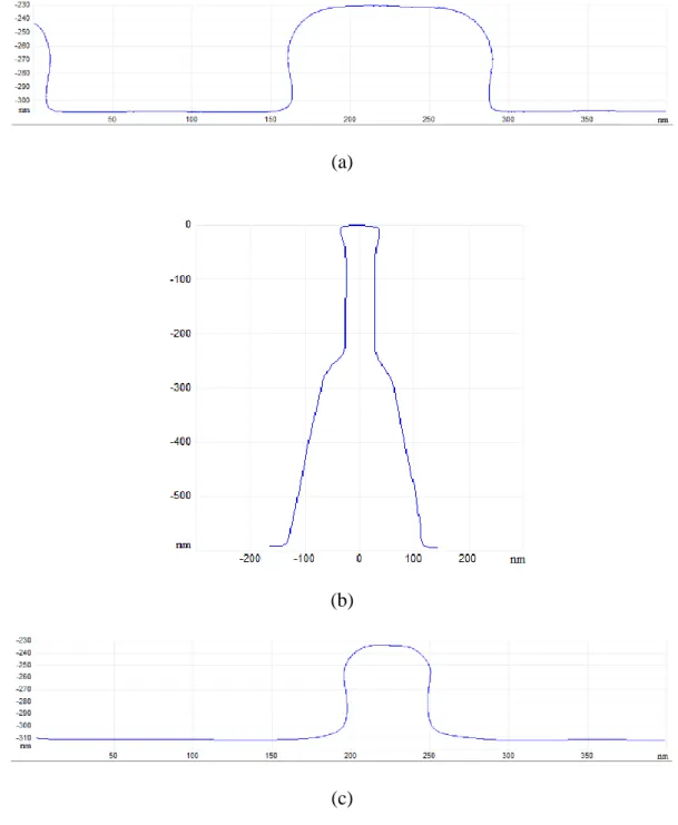
According to the type of information provided by the metrology method, there are different approaches for measuring the CD. For instance, if a top view metrology technique is used, such as the CD-SEM, the CD value may be obtained by the average value from a series of possible measurements, as illustrated in Figure 2(a). However, if the information is coming from a cross-section, the CD value may be measured in a single height of the profile, as illustrated in Figure
24
2(b). In profiles were the side walls present an angle different than 90°, it is important to well define the height where the CD is measured.
(a) (b)
Figure 2. Representation of the measurement of a CD value in a line for (a) a top view and (b) a cross-section view.
1.1.2. Line Width Roughness (LWR) and Line Edge Roughness (LER)
The patterns as exposed on a mask or a wafer present some variation on their edges. This variation, known as roughness, has an impact on the electrical characteristics of the circuits
[SHIN 2016]. For instance, the edge roughness in transistors may impact the leakage current
and may increase the threshold voltage in a transistor, impacting directly the performance of the devices [OLDIGES 2000, DÍAZ 2001, YAMAGUCHI 2004, LORUSSO 2006,
CHANDHOK 2007], in terms of timing and power consumption [KIM 2004, LEE 2004].
The roughness value may be quantified independently for each edge of the features or by evaluating the uniformity of different CD values. The first criteria refers to the evaluation of Line Edge Roughness (LER) while the second evaluates Line Width Roughness (LWR). Figure 3 (a) illustrates several different CD values that can be used to compute LWR while Figure 3 (b) shows the computation of distances between each edge position and its mean position value in order to estimate LER for both the left and right edges.
(a) (b)
Figure 3. Representation of a line and (a) the different CD values used to determine its LWR and (b) the different edge positions for computing LER for left and right edges.
25
The mathematical definition of the LWR is considered to be 3 times the standard deviation of different CD evaluations, as shown in (1).
𝐿𝑊𝑅 = 3𝜎 = 3√1
𝑁∑(𝐶𝐷𝑖− 𝐶𝐷̅̅̅̅)2 𝑁
𝑖=1
(1)
where n is the number of available CD measurements, CDi is the ith measurement value and
𝐶𝐷
̅̅̅̅ is the mean CD value from all n available measurements.
The LER corresponds to the difference, also in terms of 3 times the standard deviation, of one edge of the pattern and the mean value of the obtained measurements at the same edge. For this reason, for a given line under evaluation, two different values of LER may be computed, one for the right edge (LERR) and another for the left edge (LERL). Their computations are shown in equations (2) and (3), respectively.
𝐿𝐸𝑅𝑅 = 3𝜎𝑅 = 3√ 1 𝑁∑(𝑒𝑑𝑔𝑒𝑃𝑜𝑠𝑅𝑖− 𝑒𝑑𝑔𝑒𝑃𝑜𝑠̅̅̅̅̅̅̅̅̅̅̅̅̅)𝑅 2 𝑁 𝑖=1 (2) 𝐿𝐸𝑅𝐿 = 3𝜎𝐿 = 3√ 1 𝑁∑(𝑒𝑑𝑔𝑒𝑃𝑜𝑠𝐿𝑖− 𝑒𝑑𝑔𝑒𝑃𝑜𝑠̅̅̅̅̅̅̅̅̅̅̅̅̅)𝐿 2 𝑁 𝑖=1 (3)
where n is the number of edges position available for the evaluation, edgePosi is the ith position
of an edge and 𝑒𝑑𝑔𝑒𝑃𝑜𝑠̅̅̅̅̅̅̅̅̅̅̅̅ is the mean edge position from all n available points.
The relation between LWR and LER may vary according to the existence or not of correlation between the LER of each of the edges of a line. When the roughness of both edges are completely correlated (simultaneously fluctuate with same amplitude), the CD variation is zero, which leads to a LWR = 0, as exemplified in case (a) of Figure 4. When the roughness of both edges is in anticorrelation (edges simultaneously fluctuate with opposite amplitude), such as the example given in Figure 4 (b), the variation in CD equals 2 times the variation in edge, leading to LWR = 2 LER. Finally, the general case which is the most frequently observed is when the roughness of both edges are not correlated or present very small correlation. In this case, LWR = √2 LER, as shown in Figure 4 (c).
26
(a) (b) (c)
Figure 4. Representation of a line where in (a) both edges are completely correlated, making LWR = 0, in (b) both edges are anticorrelated, making LWR = 2 LER and in (c) both edges presenting no correlation, making LWR = √𝟐
LER.
This evaluation is performed both at wafer level and at mask level, but for different purposes. On the wafer, controlling the roughness means improving circuit performance since these variations impact the electronic behavior of the features, such as transistors. On the mask level, LER is considered to be a significant contributor to the overall feature CDU, especially for small features [WYLIE 2009].
1.1.3. Pattern Height
Another important information about features in the process of fabrication of integrated circuits is their height. The height of a feature on an integrated circuit has direct implication on its electrical behavior (conductance, capacitance – both intended and parasitic, …).
There are different ways to measure the height of a pattern. For instance, if the 3D profile of the line is available, in order to compensate for the roughness on the top of the line and eventual metrology errors, the height of the pattern may be computed as the mean value of several measurements, as shown in Figure 5 (a). If the information is coming from cross-section data, the height may be the value from the center point for instance, as shown in Figure 5 (b).
(a) (b)
Figure 5. Representation of the measurement of a height value in a line (a) for a 3D profile and (b) for cross-section data.
27
Metrology methods such as the AFM-3D, scatterometry and Transmission Electron Microscopy (TEMs) are frequently used for determining the height of a pattern.
1.1.4. Critical Dimension Uniformity (CDU):
As defined in section 1.1.1, Critical Dimension (CD) historically corresponds to the smallest dimension of a given pattern in a design. As previously noted, however, it may refer to any dimension that is considered critical for its importance on any design analysis. If one of the biggest challenges on the fabrication process of IC is achieving very small CDs, obtaining it in different spots of the mask or wafer in a uniform way is not a smaller challenge [POSTNIKOV 2003]. Hence, the metric of Critical Dimension Uniformity (CDU) is used to designate the dispersion of CD values across a given set of measurements of the same pattern
[YOSHIZAWA 2004]. This metric is important in order to control the dispersion of CD values,
both on mask and on wafer, which may lead to significant yield loss as well as reducing the optimal process window [WYLIE 2009]. The CDU can be qualitatively represented on a map describing the CD value on different places on the wafer. A CDU wafer exposure consists of exposing the same patterns across the wafer, repeating the same exposure conditions (dose and focus) in order to obtain CDU information on the wafer.
Figure 6 shows an illustration of a CDU map build from several measurements coming from different dies on a wafer.
Figure 6. Example of a CDU map, the color represents the CD value on each die
In order to illustrate the concept, consider the following example: the same pattern is exposed and measured seven times. Although this evaluation is usually performed for a much larger number of measurements, only seven are used for the sake of simplicity. Those values are shown in Table 2.
Table 2. Example of 7 measurements of the same pattern, in different locations, as a CDU evaluation illustration
1st 2nd 3rd 4th 5th 6th 7th
28
The CDU information obtained from these seven points is: average: 99.76nm, standard deviation: 1.62, minimum value: 97.8, maximum value: 102.2 and range: 4.4. This information may be useful to future considerations in several different steps of the process flow, such as in the circuit electrical characterization, process control, etc.
1.2.
Outliers
A given point in a data set is considered to be an outlier when it significantly differs from most of the other points in the data set. The sources of outlier data may vary, but they usually are related to experiment or measurement variability or error [ULLRICH 2010]. Outliers are usually classified into two categories, extreme outliers and mild outliers, according to how much they differ from the set and the level of certitude if such a point is an outlier or not
[GRUBBS 1969].
Figure 7 (a) shows a data set with most of the points clustered together and one significantly apart, which is a candidate to be considered an extreme outlier. Figure 7 (b) shows a similar situation but in this case the data set is more scattered. The indicated point is, therefore, a candidate to be considered a mild outlier. Observe, with Figure 7 (a), that classifying a given point as an outlier has no particular consideration to it being close to a given aimed value, but is a classification relative to a data set distribution.
(a) (b)
Figure 7. An example of a point that could be classified as (a) extreme outlier and (b) mild outlier
The task of determining if a given point in a set is an outlier is complex, especially when the data set is small. There are several approaches in the literature that usually rely on performing
29
an analysis on the distribution of the data points, such as the Interquartile Range (IQR) and the Median Absolute Deviation (MAD) information.
1.2.1. Interquartile Range (IQR)
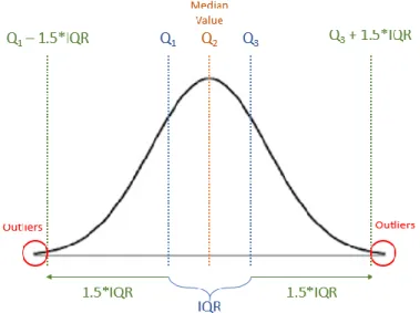
The Interquartile Range is the distance between the first and third quartiles of a distribution including 50% of the data centered on its median value (second quartile), as illustrated in Figure 8.
Figure 8. Illustration of a probability distribution in a bell shape and the positions of the first, second and third quartiles dividing the distribution into four areas of equal probability and the interquartile range
It is also called midspread by NIST, which recommends it as one of the best techniques to identify outliers [NIST 2017].
IQR is calculated as presented in (4):
IQR = Q3 − Q1 (4)
For instance, let us consider the distribution presented earlier in this chapter on Table 2. By ordering the data, we obtain Table 3
Table 3. Same data presented in Table 2, but ordered and indicating the first, second and third quartiles.
Q1 Median Q3
Measurement 97.8nm 98.4nm 98.9nm 99.1nm 100.6nm 101.3nm 102.2nm
The first and third quartiles are 98.4 and 101.3, respectively. The IQR value of this data set is 2.9.
The method to use this information to flag outliers, as first described by Tukey [TUKEY 1977], is based in evaluating each element in the data set and exclude those that are outside the range described in (5).
30
Where Q1 and Q3 are the first and third quartiles of the distribution and ω is a weighting factor
depending on the aspired confidence level. The method describes two types of outliers: extreme outlier is the one outside the range described in (5) for a ω equal to 3, while a mild outlier is the one inside the extreme range but outside the range for ω equal to 1.5. From the example in Table 2, it is possible to consider extreme outliers any measurement below 89.7nm (98.4nm – 3*2.9nm) or above 110nm (101.3nm + 3*2.9nm). Mild outliers would be any measurement below 94.05nm or above 105.65nm. Figure 9 illustrates the detection of mild outliers on the same bell distribution shown in Figure 8.
Figure 9. Illustration of a mild outlier detection algorithm based on the IQR and a coefficient 𝛚 of 1.5
Notice that this approach basically identifies as outliers any points presenting a behavior that significantly deviates from the middle 50% of the population. Although this may not be penalizing for Gaussian or near-Gaussian distributions, this method may be overly conservative (identify many outliers) for heavy-tailed distributions. In those cases, one should either adapt the weighting factor or adopt another strategy, which would consider the entire distribution, such as the Median Absolute Deviation, shown in the next section.
1.2.2. Median Absolute Deviation (MAD)
The Median Absolute Deviation (MAD) is a robust estimator of the variability of a distribution around its median value. It is defined as the median of the absolute deviations from the data median, calculated as presented in (6).
MAD = median (|𝑣𝑎𝑙𝑖− 𝑚𝑒𝑑𝑖𝑎𝑛(𝑣𝑎𝑙)|) (6)
For instance, consider the set of seven measurements presented earlier in this chapter, ordered as in Table 2.
The median value of this set is 99.1nm. When computing the distance from each point to the median value, the result shown in
31
Table 4. Distance from each point to the median value.
Q1 Median Q3
Measurement 97.8nm 98.4nm 98.9nm 99.1nm 100.6nm 101.3nm 102.2nm
Absolute Distance
to Median Value 1.3nm 0.7nm 0.2nm 0nm 1.5nm 2.2nm 3.1nm
Table 5. By ordering the resulting distribution obtained in Table 4.
Q1 Median Q3
Absolute Distance
to Median Value 0nm 0.2nm 0.7nm 1.3nm 1.5nm 2.2nm 3.1nm
And the median value of this set is 1.3nm. Therefore, the MAD value of the measurements set presented earlier is 1.3nm.
In order to use this value for identifying and removing outliers, only the data inside the range given by (7) is considered valid [SEO 2006]:
[𝑄1 − ω κ MAD, Q3 + ω κ MAD] (7)
Where ω is a weighting factor depending on the aspired confidence level and κ is a constant scale factor used to estimate the standard deviation of a distribution from its MAD value. For instance, a normal distribution has its κ factor equal to 1.4286, as demonstrated by Seo
[SEO 2006].
On the presented example, considering the hypothesis that the measurements presented in Table 2 are expected to respect a Gaussian distribution, an extreme outlier would be considered a measurement below 92.83nm (98.4nm – 3*1.4286*1.3nm) or above 106.87nm (101.3nm + 3*1.4286*1.3nm) while a mild outlier ω = 1.5) would be below 95.61nm or above 104.09nm. The main advantage of this approach, in comparison to the IQR based strategy, is that it accounts for the entire distribution, not only the centered 50% of it. However, this may also be considered inconvenient since outlier values are considered in the evaluation and may impact their own detection.
1.3.
Precision
Precision is a term that refers to the closeness of agreement between different test results. This term is relevant because presumably identical experiments may yield non-identical results
[DIEBOLD 2001]. This fact gives rise to the concept of variability, which may be defined as
the tendency of different measurement tests to produce different values under same conditions or conditions that are varying over time [NIST 2017]. The importance of precision is highlighted when observing changes or evolution in a process. For instance, when evaluating the effects of a change in the etching recipe or of the exposure strategy. Achieving a high level
32
of precision, even with some inaccuracy, enables to follow the evolution or the drift of a process.
An illustration of two distributions, one (a) showing a low precision and another (b) showing a high precision is presented in Figure 10.
(a) (b)
Figure 10. An example of a set of points (a) with low precision and (b) presenting high precision.
The precision of any given method is usually presented in terms of standard deviation. The smaller the standard deviation, the more precise the method. For this reason, let us consider the precision as a metric for non-systematic error (also known as random error or statistical error). This type of error may be considered the result of process measurement fluctuation. Therefore, the larger the statistical error of a metrology method, the less precise it is.
The concept of precision is related to short-term and long-term variation of measurements and is also related to a way of distinguishing different types or sources of variation, which in turns is related to the concepts of repeatability and reproducibility [NIST 2017].
Apart from differences on the samples being measured, some other important factors are considered when evaluating the precision of a given method:
a) the operator;
b) the equipment used;
c) the calibration of the equipment;
d) the environment (temperature, humidity, pressure, etc.); e) the time elapsed between measurements.
1.3.1. Repeatability
Repeatability accounts for the variability measured under controlled conditions, that is, when the same operator measures multiple times using the same equipment, calibrated the same way
33
under controlled environmental conditions over a short period of time (the definition of short-term may vary according to the type of evaluation performed but, in the context of metrology it is typically considered to be within the same day). Short term and long term variability are important metrics of metrology stability. In this context, two types of repeatability, both of which are commonly used to characterize semiconductor equipment, can be described: static repeatability and dynamic repeatability [SENDELBACH 2010].
1.3.1.1. Static Repeatability
In a static repeatability exercise, the wafer is moved into the tool, alignment and pattern recognition are performed, and then multiple measurements are conducted while the wafer remains motionless, or “static”). The wafer is removed from the tool only at the end of the exercise. Static repeatability measurements are almost always conducted on a short-term basis, as it is impractical to keep a wafer inside a tool for a long period of time. Static repeatability can provide important information related to tool noise, for example, since all the other conditions are kept stable.
1.3.1.2. Dynamic Repeatability
As opposed to static repeatability, in a dynamic repeatability experiment the wafer is removed from the tool after each measurement (or after a set of measurements, with each measurement performed at a different location on the wafer). This is typically done by running the same measurement recipe multiple times. In this case, wafer alignment and pattern recognition variation will affect the measurement results. Thus, comparing static and dynamic repeatability results can give information about the effect of alignment and pattern recognition capabilities of the equipment on the measurement. In short, dynamic repeatability measurements can provide information regarding the robustness of the tool when repeating the same measurement under realistic situations.
1.3.2. Reproducibility
In contrast to repeatability, reproducibility is the total measurement precision, including the effects of long-term variability [NIST 2017]. It may include using different equipment, calibrated differently, under different environment conditions and so on. These situations are generally accepted to be less likely to generate similar results than if they are held constant (as is done for repeatability). In the semiconductor industry, the term “reproducibility” is not often used. This is due to multiple factors, including:
a) manufacturing equipment is highly automated, making the “operator” variable less important;
b) variation due to equipment factors (type, calibration, etc.) falls under another separate category called “tool matching” [ZERBE 2007];
c) environmental conditions in which wafers are measured are tightly controlled, making this factor less important;
34
1.4.
Accuracy
Although there are different definitions and types of accuracy, all of them imply the comparison of a measurement or set of measurements to some form of standard. This standard can sometimes be a value or set of values that are targeted by the experimenter using the equipment that produces the measurement samples – often called the process equipment. For example, the values can be dose settings from a lithography system used to vary the CD among the samples, or etch times from an etch system used to create trenches of varying depths. In such instances, the parameter units from the process equipment are not necessarily the same as those that are measured by the metrology system. In the examples above, dose is often reported in units of (energy / area) and the etch time is in units of time, while the measurement systems measure the line CDs and trench depths in units of length.
More often, the standard comes from the measurement of the samples using a reference system, sometimes called a Reference Measurement System (RMS). Traditionally, the definition of accuracy is simply the difference in measurement value between the RMS and the measurement system being evaluated. This difference is also called the offset or bias. For a set of samples, the difference between the average measurement value from the RMS and the average measurement value from the system under evaluation is called the average offset
[SENDELBACH 2003].
Although this definition of accuracy is a good start, it does not capture some important attributes of a good measurement. One of these attributes is the ability of the system under evaluation to be sensitive to changes in the parameter being measured. For example, if the RMS detects an increase in line CD from one sample to the next, the system under evaluation will also detect an increase. The tracking of the RMS measurements by the measurements of the system under evaluation is preferred to be linear, as both systems are nominally measuring the same thing [SENDELBACH 2006]. A representation of the concept is shown in Figure 11. Furthermore, when plotting both sets of measurements and determining a best-fit line between them, it is preferred that this line has unity slope. If the tracking is linear with a perfect correlation (R2 = 1) and unity slope, then the offset between the systems is constant.
Figure 11. A representation of a linear tracking of the RMS measurements by the measurements of the system under evaluation.
Another important attribute of a good measurement is that it is insensitive to changes in secondary characteristics. Secondary characteristics are those parameters of the sample that
35
ideally should not affect the measurement of the parameter of interest. Because many metrology methods in the semiconductor industry are susceptible to cross-correlations between measurement parameters, this attribute is not merely of academic interest, but is crucially important for modern semiconductor metrology systems. A common example of sensitivity to changes in secondary characteristics is the frequent effect of changes of sidewall angle of a line to the measurement of the line’s CD, as measured by CD-SEM or scatterometry systems. Adoption of these attributes of a good measurement provide a more comprehensive definition of accuracy; however, they also spawn two additional types of accuracy: relative accuracy
[SENDELBACH 2010] and absolute accuracy. Relative accuracy incorporates both of these
attributes (ability to track changes in the parameter of interest, preferably linearly and with unity slope, while being insensitive to changes in secondary characteristics) without regard to the average offset [SENDELBACH 2004]. Most semiconductor metrology systems in manufacturing need to detect shifts in the parameter of interest without the requirement of providing a minimal average offset, and thus are required to have good relative accuracy. Note that there is no overlap in definition between relative accuracy (where average offset is irrelevant) and the traditional definition of accuracy (where offset, or average offset, is the only characteristic that matters).
Like relative accuracy, absolute accuracy also requires the ability to track changes in the parameter of interest while not being affected by secondary characteristic changes. In addition, absolute accuracy takes into account the average offset between the RMS and the system under evaluation. Thus, in order for a system to have a good absolute accuracy, this average offset must be minimized. One example of this is when the decision, along with the resulting action, with respect to the set of samples depends on the average offset. One example in the semiconductor industry where absolute accuracy is important is the measurement of photoresist line CDs during the evaluation of an optical proximity correction (OPC) adjustment to a lithography reticle [RANA 2010].
37
39
2. Metrology Methods
Metrology is the science of performing measurements, i.e., assigning a numerical value to a characteristic of an object or event. Metrology tools and methods vary significantly according to the field of application and to the nature of the object or event to measure. The semiconductor industry is usually interested in measuring geometrical, electrical or magnetic quantities, among others. In this work, the term metrology usually refers to obtaining geometrical quantities of samples.
There are different metrology techniques available for the semiconductor industry to determine geometrical characteristics of patterns. All these techniques present strong and weak points that make them more suitable for some types of applications than for others. In this chapter, four of the most frequent metrology techniques used by the semiconductor industry are presented and discussed: CD-SEM, AFM-3D, scatterometry and FIB-STEM. Finally, a comparison among these methods is also presented.
2.1.
CD-SEM
An electron microscope is a microscope that uses an accelerated beam of electrons to create an enlarged image of a sample. In comparison to an optical microscope using light, the usage of electrons ensures a much higher magnification and resolution. This is due to the effective wavelength of the electron beam (< 1nm) compared to the 400nm – 700nm wavelength of the visible light used on optical microscopes. For this reason, the typical resolution of an electron microscope is of 0.5nm to 1nm, while the optical microscopes have typical resolution of 200nm
[IKEGAMI 2011]. The maximum magnification of the specimen’s image is also very different.
While an optical microscope may reach typically between x1000 and x2000, an electron microscope may go beyond x100000.
Among several variants, a very popular one in the field of microelectronics is the Scanning Electron Microscope (SEM). This is an electron microscope which produces images by scanning the surface of the sample with an electron beam. As the beam scans the surface, the retrieved information by the sensors are stored according to the coordinates X and Y of the incident beam. This provides information about the topography and composition of the scanned sample.
A CD-SEM (Critical Dimension Scanning Electron Microscope) is the name given to a SEM system dedicated to measure the dimensions of fine patterns. These tools usually operate in low energy (1keV or less) in order to preserve the sample [SULLIVAN 2003]. Moreover, these tools can provide automated measurements based on metrology recipes in order to provide fast measurements of different locations on the sample.
The literature proposes some very detailed books to explain the techniques of the Electron microscope [VILLARRUBIA 2004, CEPLER 2012, MACK 2015]. In this section, some details on the electron-matter interactions and the different signals used for imaging samples
40
(Secondary electrons and Backscattered electrons) are presented. Moreover, the basic structure of a CD-SEM and how the image is generated are presented as well. Finally, the advantages and disadvantages of this metrology technique are presented.
2.1.1. Electron-matter interactions
When the electrons from the primary incident beam strike the specimen, they penetrate inside the matter and interact both elastically and inelastically with the atoms of the sample
[HOVINGTON 1997, BABIN 2003]. Elastic scattering is when the incident electron does not
lose energy while interacting with the material. Inelastic scattering, in the contrary, are the interactions that cause energy loss. The electron-matter interactions generate different signals that can be detected by different sensors on the tool. Some typical examples are Auger electrons, secondary electrons (SE), back-scattered electrons (BSE), Photons (cathodoluminescence - CL) and characteristic X-rays. If the sample is thick, no electron will be transmitted but, in the case of thin samples, it is possible to detect electrons on the other side of the specimen, either the directly transmitted ones or the elastically or inelastically scattered ones [DROUIN 2007]. Figure 12 (a) shows the generated signals by an electron beam incident onto a thick sample while Figure 12 (b) shows the signals from a thin sample.
(a) (b)
Figure 12: Signals generated by the interaction of an incident beam of electrons and (a) a thick sample and (b) a thin sample.
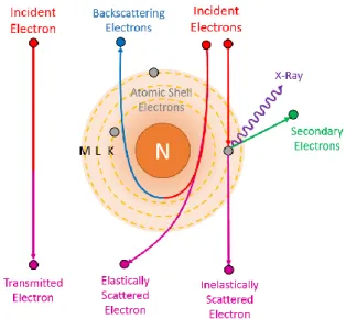
The combining effects of elastic and inelastic scattering events control the penetration of the electrons into the sample [RIO 2010]. Moreover, those effects impact directly the generation of secondary and backscattered electrons, as well as the observed contrast. A particle model of the different events that may occur with incident electrons as they interact with the matter is shown in Figure 13, based on the Bohr atom model.
41
Figure 13: Schematic of interactions that may occur with the incident electrons.
Each incident electron is affected by multiple events in its way through the material. Elastic scattering events may produce backscattering electrons while inelastic scattering events lead to energy loss, slowing down the incident electron until it is absorbed, unless it is transmitted across the material [KYSER 1974]. Moreover, inelastic events also produce secondary electrons, Auger electrons and X-rays, among others.
As previously stated, as the scanning electron beam impacts the sample, several different signals are emitted. Each individual signal may be associated to a different region from which it is produced, called volume. This interaction volume of the primary electrons describes the range and the spatial distribution, and depends on the composition of the sample and on the accelerating voltage. Figure 14 shows an illustration of the interaction volume of the incident electron diffusion and the different signals it generates.
42
In principle, any of the signals generated at the sample surface can be detected and used for different purposes, which enables the SEM tool to be applied to a wide range of applications in different fields. As it is illustrated in Figure 14, these particles come from different parts of the sample. Besides coming from different regions, these signals vary significantly in terms of the number of particles and their energy, as seen in the energy spectrum of electron emission N(E), in arbitrary units, presented in Figure 15.
Figure 15: Energy spectrum of electron emission N(E) in arbitrary units. Regions of secondary electrons (SE) and backscattered electrons (BSE) are indicated [BELL 2012].
Figure 15 shows that there is a large number of electrons that are concentrated at the low energy part of the distribution, the secondary electrons. Moreover, backscattering electrons present a large range of possible energies and their interval also includes the energy levels of Auger electrons.
2.1.2. Scanning Electron Microscope Structure
In a typical SEM, an electron beam is emitted from a gun that contains a tungsten filament. A voltage is applied to the filament, acting like a cathode, which heats up. Electrons are emitted from the filament thermionically. An anode plate is present close to the filament, creating a strong electric force that causes the electrons to accelerate towards the anode plate. The electrons pass the anode plate and go down the column of the microscope.
The electrons are then focused by the electromagnetic lens to form a narrow beam over the sample. Finally, this beam passes by an electromagnetic deflector that controls the back and forth scan of the beam over the specimen that is over a stage inside the chamber, in vacuum. A schematic of a standard SEM is shown in Figure 16.
Finally, inside the chamber the sensors placed in different locations may collect the different signals coming from the sample in order to form the image. The way the image is formed is the topic of the next section.
43
Figure 16: Schematic of a standard Scanning Electron Microscope.
2.1.3. Image Formation
The image generated by a SEM is a 2D intensity map. Each pixel corresponds to a point on the sample, representing the intensity of the signal captured by the detector while the beam was striking that specific point. For this reason, a SEM image is an electron synthesis and not an optical transformation, as occurs in an optical light microscope. The beam is then moved to the next position where a new acquisition is performed. The beam scans the sample as indicated by the raster strategy, which may vary according to the scan mode selected.
Figure 17 (a) shows a representation of a raster strategy while Figure 17 (b) shows the resulting image after completing the scan.
44
(b)
Figure 17: (a) Representation of a raster strategy and (b) the resulting image.
In a standard image acquisition, the scan is repeated a few times over the same sample. Each passage of the beam over the sample generates new data to the sensors, which store them as a new image frame. Each pixel value in the final image is actually the average of the pixel values from each scan.
2.1.3.1. Image Magnification and Resolution
2.1.3.1.1.
Magnification
Counter to optical microscopes, the magnification in a SEM does not depend on the objective lens used. Instead, the magnification of a SEM image is generated by the ratio between the dimensions of the raster on the specimen and the raster on the display, as shown in Equation (8). Considering that the display size is constant, increasing the magnification means reducing the size of the specimen that is scanned.
𝑀𝑎𝑔 = 𝐷𝑖𝑠𝑝𝑙𝑎𝑦 𝑅𝑎𝑠𝑡𝑒𝑟 𝐷𝑖𝑚𝑒𝑛𝑠𝑖𝑜𝑛
𝑆𝑝𝑒𝑐𝑖𝑚𝑒𝑛 𝑅𝑎𝑠𝑡𝑒𝑟 𝐷𝑖𝑚𝑒𝑛𝑠𝑖𝑜𝑛 (8)
Figure 18 illustrates how a smaller scan area Figure 18 (a) leads to each pixel on the display to correspond to a smaller area of the specimen, increasing the magnification on the generated image. On the contrary, a larger scan area on the sample leads to larger pixel sizes, reducing the image magnification, as shown in Figure 18 (b).
45
(a) (b)
Figure 18: (a) High magnification acquisition and (b) low magnification acquisition.
It is worth noticing that the limit to SEM magnification is given by its resolution. Any further increase on the number of pixels per nm will only result in the artifact of “empty magnification”. Empty magnification is the effect of increasing the pixel resolution of a region without improving the acquired level of information. Its effect is equivalent to a digital zoom, i.e., one pixel of significant data is split in four pixels containing the same information.
2.1.3.1.2.
Resolution
The resolution is defined as the ability to distinguish two neighboring points. The resolution of a SEM is driven by the beam spot size. The beam spot size itself is a function of the wavelength of the electrons and of the electron-optical system that generates the scanning behavior of the beam.
The limit resolution (r) may be described as shown in Equation (9):
𝑟 = 𝜆
2𝑁𝐴 (9)
Where λ is the wavelength of the beam and NA is the numerical aperture of the lens.
Considering the quantum mechanical properties of an electron, its wavelength (λ) is defined by the Broglie relationship, shown in Equation (10):
𝜆 = ℎ 𝑝=
ℎ √2𝑚0𝐸
(10)
Where h is the Planck constant, m0 is the rest mass of the electron, p is the electron momentum and E is the accelerating voltage.
Considering that the electrons moving on the microscope are at high speeds (defined by the accelerating voltage of the electron gun), the Equation (11) may be expressed with its relativistic version:
46
𝜆 = ℎ𝑐
√2𝐸𝐸0+ 𝐸2
(11)
Where E0 is the rest energy.
These equations show that the wavelength increases when the energy decreases. And, since the resolution is proportional to the wavelength (as shown in Equation (9)), it means that to improve the resolution, the energy must be as high as possible.
Figure 19 shows quantitatively the impact of acceleration voltage on the wavelength. For larger acceleration voltages (see Figure 19 (a) for energies above 5keV), the wavelength is below 20pm, while images acquired using 0.3kV would be limited to a wavelength of 71pm. This can be considered still a sufficiently small value, considering the target dimensions. However, the wavelength is not the only limitation on resolution, as it is presented in the next section.
(a) (b)
Figure 19: Wavelength as a function of the acceleration voltage. (a) Range from 1kV to 40kV and (b) range from 0.1kV to 1kV.
Other factors include the aperture size and the working distance, for instance.
2.1.3.2. SEM Signals for Image Formation
Among the different signals generated by the electron beam striking the sample material inside the chamber of a SEM, the most frequently used to generate images are the backscattered electrons (BSE) and the secondary electrons (SE). Those two signals are discussed in the next two sections. Other signals, such as x-rays, photons, etc., may also provide significant information of the specimen in some circumstances. These signals are briefly discussed in the next sections as well.
2.1.3.2.1.
Backscattered Electrons
Backscattered electron (BSE) signal is generated by the incident beam electrons after undergoing elastic and inelastic scattering events on the sample material as shown in Figure 13.
The ratio between the number of electrons sent by the primary beam and the ones that leave the sample with an energy above 50eV (threshold below which electrons are no longer considered backscattered) is known as the backscattering coefficient (η). The SEM sensor for
47
BSE counts the number of electrons detected, and not their energy. Therefore, the detected signal is proportional to the backscattering coefficient.
BSE signals are usually used for imaging what is known as compositional contrast. Since areas with different composition will produce a different number of backscattered electrons, one may rely on this information to identify different areas.
The behavior of backscattered electrons can be separated in two cases, one for energies higher than 5keV and another for energies below 5keV. In the first case, the backscattering coefficient increases monotonically with the incident angle of the beam, with the increasing atomic number of the sampling material (Z), as shown in Figure 20 [REIMER 2013]. In this case, regions of high average atomic number (Z) will appear bright relatively to regions with average low atomic number.
Figure 20 : Backscattering coefficient as a function of the electron energy in the range 1–30keV [REIMER 2013].
The contrast (C) between two regions A and B may be determined as the difference between their backscattering coefficients, ηA and ηB, as shown in Equation (12):
𝐶 = (𝜂𝐴− 𝜂𝐵) 𝜂𝐵
(12)
However, for energies below 5keV, the behavior is not monotonic and varies significantly according to the specimen material. This change in behavior is mainly due to the elastic cross-section. Figure 21 shows the coefficient of backscattered electrons as a function of the energy for energies below 2keV for different materials.

![Figure 21 : Elastic backscatter coefficient for different materials as a function of the electron energy [SCHMID 1983]](https://thumb-eu.123doks.com/thumbv2/123doknet/12845233.367481/49.892.267.634.107.384/figure-elastic-backscatter-coefficient-different-materials-function-electron.webp)
![Figure 39: An illustration of the three different AFM modes, Tapping, DT and CD [SU 2015]](https://thumb-eu.123doks.com/thumbv2/123doknet/12845233.367481/63.892.134.779.112.345/figure-illustration-different-afm-modes-tapping-dt-cd.webp)