i
THÈSE
En vue de l’obtention du
DOCTORAT DE L’UNIVERSITÉ DE TOULOUSE
Délivré par l'Université Toulouse 3 - Paul Sabatier
Présentée et soutenue par
Precious Manti RADINGOANA
Le 5 décembre 2019Titre:
Densification et caractérisation microstructurale de céramiques à base de ZnO
obtenues par frittage SPS pour application
thermoélectrique
Ecole doctorale: SDM - SCIENCES DE LA MATIERE – Toulouse Spécialité: Sciences et Génie des Matériaux
Unité de recherche:
CIRIMAT - Centre Interuniversitaire de Recherche et d'Ingénierie des Matériaux
Thèse dirigée par
Sophie GUILLEMET-FRITSCH Claude ESTOURNES
Jury:
Guillaume BERNARD-GRANGER Directeur de Recherche, CEA Rapporteur Bertrand LENOIR Professeur, Institut Jean Lamour Rapporteur Bénédicte WAROT Directeur de Recherche, CEMES/CNRS Examinatrice Sophie GUILLEMET-FRISTCH Directeur de Recherche, CIRIMAT/CNRS Directrice de thèse Claude ESTOURNES Directeur de Recherche, CIRIMAT/CNRS Co-directeur de these Peter Apata OLUBAMBI Professeur, University of Johannesburg Invité Jacques NOUDEM Professeur, CRISMAT Invité
ii
Abstract
The pursuit of better thermoelectric properties using ZnO has been hampered by the high thermal conductivity and low electrical conductivity of this low cost and environmental friendly material. The present study focuses on the synthesis and spark plasma sintering of zinc oxide composites to improve these thermoelectric properties. Pure and Al (2at %) doped ZnO powder were synthesized using co-precipitation followed by calcination. Further, the synthesized Al-doped ZnO powder was mixed with low concentrations of polyaniline (PANI) powder to reduce the thermal conductivity. The powders were sintered using Dr Sinter 2080 unit by varying different parameters: temperature (250-900°C), pressure (100-250 MPa), sintering atmosphere (air and vacuum), point of pressure application, holding time and current isolation. The ceramics were finally annealed at 600°C in air.
The densification and the microstructure properties of pure ZnO ceramics were studied. It was illustrated that SPS can sinter to high densities irrespective of starting powder. The characteristics of the ceramics prepared from both synthetic and commercial ZnO powder were compared. Both could be fully densified above 99% at a temperature as low as 600°C. The sintering atmospheres (air and vacuum) and electric current (with or without) did not affect the densification. However, grain size difference of about 8 µm was observed when sintering with or without current. A guide for controlling the densification and the grain size of ZnO ceramics obtained by spark plasma sintering of dried powders was developed. Annealing at 600°C does not have significant effect on the microstructure of ZnO ceramics, however, affects the oxygen stoichiometry, and hence modified the electrical behaviour such that the resistivity of the pure ZnO ceramics increased by two orders of magnitude. As-sintered ceramics prepared from synthetic powder show the best thermoelectric performance as compared to annealed ceramics with a ZT of 8x10⁻³ at 500°C because of low electrical resistivity and high Seebeck Coefficient. This signifies the importance of the synthesis process in determining the thermoelectric properties.
The thermal conductivity and electrical resistivity of ZnO ceramic were improved by doping with 2 at% Al. The powder grain size reduced from 177 to 75 nm when Al is present. Maximum relative density of 98.9% was achieved at a temperature of 650°C and a pressure of 250 MPa. The grain size of the sintered ceramics reduced from 5.4 µm to <1 µm. Secondary phases, ZnAl2O4 and Al2O3, are formed because of excess Al when the axial pressure was
iii improved in electrical conductivity which caused a decrease in the absolute Seebeck Coefficient as a result of increased carrier concentration. The reduction in the grain size lead to a decrease in the thermal conductivity due to phonon scattering at the grain boundaries. As a result, ZT of 1.5x10⁻³ at 500°C was obtained.
The influence of dispersed PANI in Al-doped ZnO ceramics was investigated. Using SPS, high densification of 98.5% and 97.3 % was achieved at a temperature as low as 250°C for 5wt% and 9wt% PANI, respectively. As a result, the nanostructure of the ceramics was maintained. Thermal conductivity below 6 W/mK was achieved by incorporating PANI into Al-doped ZnO ceramics. The resistivity was also slightly improved and high Seebeck Coefficient was kept, due to energy filtering. Maximum ZT of 0.8x10⁻³ was achieved at 190°C using 9wt% PANI compared to 0.06x10⁻³ for 0 wt% PANI. This study has opened opportunities for development of ZnO based polymer composites at low temperatures using spark plasma sintering.
Keywords: ZnO, Spark plasma sintering, Thermoelectricity, Ceramics, Polyaniline, Aluminium
iv
Acknowledgements
The research associated with this PhD thesis commenced in January 2016 at Centre Inter-Universitaire de Recherche et d’Ingénierie des Matériaux (CIRIMAT) laboratory. In completing this programme I am grateful to many people, who have inspired, encouraged, supervised, supported and helped me over the time of the research, my stay in France and during the writing of this thesis. I would like to extend my warmest gratitude to my supervisors, Dr Sophie Guillemet-Fritsch and Prof. Claude Estournès, for their excellent supervision, persistent help, skilful and excellent guidance, positive encouragement and most of all, their unwavering patience in bringing me back to track when occasionally falter.
This programme would not have been possible if it was not to the initiatives of Prof. P.A Olubambi to collaborate with the CIRIMAT laboratory. Thank you for having faith in me. I am grateful for your emotional support and the expertise shared in this thesis.
I acknowledge the financial support of A European and South African Partnership on Heritage and Past+ (AESOP+, Europe) and National Research Fund (NRF, South Africa) for providing an opportunity to do research studies at CIRIMAT laboratory.
I am thankful to the director of CIRIMAT laboratory, Prof. Christophe Laurent, for accepting me in the laboratory to use the facilities towards my research studies. I would also like to thank my colleagues at CIRIMAT laboratory for their friendship and individual help during my time here. I appreciate the technical support of Marie-Claire, Geoffroy, Benjamin, Jean-Jacques, Christopher, Isabelle, Vincent, and Abdérahmane. I am thankful for the general logistics and administrative support of Maryse, Jessie, Nabila and other administrative stuff. I am grateful to my officemates for creating a pleasant working environment, support and assistance towards the research studies of this thesis: Veronique, Nahum, Elsa, Thi Mong Cam, Vignesh, Thi Ly, Mai Doo and Zifeng. Also, thanks for the support of Yohan, Inthunga, Juliano, Juliana, Glenda, David, Driss, Arnaud, Yannick and other CIRIMAT colleagues.
I am thankful to Laboratoire de Cristallographie et Sciences des Matériaux (CRISMAT) for allowing me to do my thermoelectric measurements and other analysis at their laboratory. The members at CRISTMAT made the working environment to be pleasant during my stay, it is very much appreciated. I appreciate and acknowledge the technical assistance of J. Lecourt
v and C. Bilot. Foremost, I am grateful for the short term supervision of Prof. Jacques Noudem for all his assistance and expertise.
My dearest friends, Dr O.M Olabanji, Dr G Chimowa and Dr S Diouf, are gratefully acknowledged for their contributions towards compilation of this thesis. I am also grateful to Prof K. Mpofu for allowing me to using their premises at Tshwane University of Technology during the last part of my thesis.
Apart from work, I am thankful to my friends: Aluwani, Ntombi, George and Miltia for making my stay in Toulouse to be such a wonderful experience. I appreciate all your emotional support and positive encouragement; you have made my PhD journey to be bearable. Also, grateful to my friends during my stay in South Africa for the last months of my thesis for all their assistance: Eddie Thaba and Tshepo Mahanuke.
I would like to express my heartfelt thanks to my loving family for their great support towards my dreams. Thank you for being the pillars of my strength, the encouragement you gave me through this programme is well appreciated.
Finally, I thank the almighty God for the strength and wisdom he gave me to conclude this study.
I will forever cherish the experience of studying in France.
Much thanks,
Radingoana Precious Manti Université Paul Sabatier, Toulouse
vi
Table of Contents
Abstract ... ii
Acknowledgements ... iv
List of tables ... x
List of figures ... xi
List of symbols ... xvi
General introduction ... 2
1.
Bibliography ... 5
1.1 Thermoelectricity fundamentals ... 5
1.1.1 Thermoelectric effects (Seebeck and Peltier effect) ... 5
1.1.2 Performance of thermoelectric materials ... 8
1.2 Current state-of-the-art thermoelectric materials ... 14
1.3 Metal oxide thermoelectric materials ... 15
1.4 ZnO based thermoelectric materials... 17
1.4.1 Characteristics and challenges of pure ZnO ... 17
1.4.2 Challenges with preparing nanostructured pure ZnO ceramics ... 18
1.4.3 Intrinsic ZnO defects ... 21
1.4.4 Doped and co-doped ZnO TE properties ... 24
1.4.5 Influence of grain morphology on thermoelectric properties of Al-doped ZnO .... 26
1.4.6 Doping of metal oxides with conducting polymers ... 29
1.4.7 Low temperature sintering of ZnO based ceramics ... 34
1.5 Summary ... 37
2.
Experimental techniques ... 39
2.1 Synthesis of pure and Al-doped ZnO powders ... 39
2.2 Preparation of polymer doped ZnO based powders ... 40
2.3 Consolidation of ZnO based ceramics ... 41
2.3.1 Background on spark plasma sintering equipment ... 41
2.3.2 Sintering of pure ZnO ... 42
vii
2.4 Characterization techniques ... 46
2.4.1 X-ray diffractometer ... 46
2.4.2 Microscopy analysis... 46
2.4.3 Particle size and relative density measuring techniques ... 47
2.4.4 Thermal analysis (TGA-DSC) ... 48
2.4.5 Spectroscopy analysis ... 48
2.5 Electrical transport properties ... 48
2.5.1 Resistivity and Seebeck Coefficient measurements ... 48
2.5.2 Thermal conductivity measurement ... 50
2.5.3 Hall Effect measurements ... 51
2.5.4 Band gap measurements ... 52
3.
Influence of processing parameters on the densification and the
microstructure of pure zinc oxide ceramics prepared by spark plasma
sintering ... 55
3.1 Introduction ... 55
3.2 Experimental method and procedure ... 57
3.3 Results and discussion ... 57
3.3.1 Characterization of the commercial ZnO powder ... 57
3.3.2 Spark plasma sintering of ZnO ceramics ... 60
3.4
Conclusions ... 70
4.
Thermoelectric properties of ZnO ceramics densified through spark
plasma sintering ... 72
4.1 Introduction ... 72
4.2 Materials and methods ... 72
4.2.1 Synthesis of ZnO particles ... 72
4.2.2 Densification of ZnO by Spark plasma sintering (SPS) ... 73
4.2.3 Electrical measurements ... 73
4.3 Results and discussion ... 74
4.3.1 Characterization of synthetic zinc oxide powders ... 74
viii
4.3.2 Spark plasma sintering of pure ZnO ceramics ... 79
4.3.3 Influence of annealing treatment on the microstructure of ZnO ceramics ... 88
4.3.4 Thermoelectric properties of pure ZnO ceramics ... 90
4.4 Conclusions ... 98
5
Microstructure and thermoelectric properties of Al-doped ZnO
ceramics prepared through spark plasma sintering ... 100
5.1 Introduction ... 100
5.2 Materials and methodology ... 101
5.2.1 Synthesis of Zn0.98Al0.02O powder ... 101
5.2.2 Spark plasma sintering of the Zn0.98Al0.02O powder ... 101
5.3 Results and discussion ... 101
5.3.1 Characterization of synthetic Al-doped ZnO powders ... 101
5.3.2 Spark plasma sintering of Al-doped ZnO powder ... 105
5.3.3 Thermoelectric properties ... 114
5.4 Conclusions ... 118
6
Spark plasma sintering of polyaniline dispersed in Al-doped ZnO
ceramics for thermoelectric application ... 121
6.1 Introduction ... 121
6.2 Materials and methodology ... 122
6.2.1 Preparation of Zn0.98Al0.02O /Polyaniline powder ... 122
6.2.2 Spark plasma sintering of Zn0.98Al0.02O /Polyaniline powder ... 122
6.2.3 Characterization of Zn0.98Al0.02O /Polyaniline powders and ceramics ... 122
6.2.4 Electrical properties of Zn0.98Al0.02O /Polyaniline ceramics ... 123
6.3 Results and discussion ... 123
6.3.1 Characterization of mixed powders of Al-doped ZnO and Polyaniline ... 123
6.3.2 Characterization of sintered Al-doped ZnO/PANI ceramics ... 129
6.3.3 Thermoelectric properties of sintered ceramics ... 134
6.4 Conclusions ... 140
Conclusions and recommendations ... 142
ix
Recommendations ... 143
References ... 144
Appendix ... 164
Appendices A : Heat capacity measurements ... 165
x
List of tables
Table 1.1 Thermoelectric properties of pure ZnO ceramics at 700K ... 20
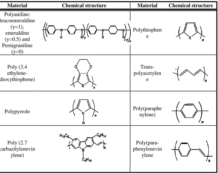
Table 1.2 Chemical structure of few conducting polymers [144] ... 30
Table 1.3 Thermoelectric properties of conducting polymers, re-tabulated from Du et al. [144]. ... 30
Table 1.4 Characteristics of ZnO ceramics sintered below 400°C ... 36
Table 2.1 Sintering conditions of ZnO and ZnA/PANI ceramics ... 44
Table 3.1 Relative density and grain size of ceramics prepared from commercial ZnO powder for different sintering conditions [Symbols: SC is sintering cycle and RT is room temperature] ... 61
Table 4.1 Specific surface area and grain size of synthetic and commercial ZnO powders .... 77
Table 4.2 Relative density and grain size of ceramics prepared from com-ZnO and synthetic ZnO powder for different sintering conditions [Symbols: CCP : ceramics prepared from commercial ZnO powder, CSP : ceramics prepared from synthetic ZnO powder, SC : sintering cycle and RT : room temperature] ... 82
Table 4.3 Electrical parameters measured at room temperature of as-sintered ZnO ceramics 92 Table 5.1Surface area distribution and particle size of pure and Al-doped ZnO powders .... 104
Table 5.2 Summary of pure and Al-doped ZnO ceramics characteristics for varied SPS parameters (Note: RT-Room temperature, HT- Holding time)... 107
Table 6.1 Relative density of sintered Al-doped ZnO/PANI ceramics ... 131
Table 6.2 Determined physical properties of Al-doped ZnO/PANI ceramics ... 136
xi
List of figures
Fig. 1.1 Comparison between Seebeck and Peltier effect [5]... 6
Fig. 1.2. Illustration of Seebeck effect [6]: Migration of charge carriers from hot to cold side on n- and p-type (a) and the building up of internal electric field (b). ... 6
Fig. 1.3 Typical example of thermoelectric module[14] ... 8
Fig. 1.4 Power generation efficiency versus temperature for different energy conversion technologies [15] (Note: org-Organic, CSP-concentrated solar power, PV- photovoltaic, TE- thermoelectric, TI-Thermionic) ... 10
Fig. 1.5 Figure of merit and behavior of thermoelectric parameters at varying carrier concentration [21] ... 11
Fig. 1.6 Effect of thermal conductivity on the figure of merit [14] ... 13
Fig. 1.7 Effect of grain size on thermal conductivity as a function of temperature on nano-grained Ga-ZnO ceramics [44] ... 13
Fig. 1.8 Scattering mechanism of phonons within a nanostructured material [27] ... 14
Fig. 1.9 Recent advances of different thermoelectric materials: n-type materials[22] (a), p-type materials [22] (b) and n & p-type of recent thermoelectric materials [66] (c) ... 15
Fig. 1.10 Recent progress on thermoelectric properties of metal oxides. ZT versus temperature for (Bi0.875Ba0.125CuSeO[29], Ca2.7Ag0.3CoO9/10wt%Ag [71], Ca2.8Ag0.05Lu0.15Co4O9+δ[70], Na1.7Co2O4[72], Na1.7Co2O4/10wt%Ag [72], Ca0.9(Dy,Yb)0.1MnO3 [74], Ca0.9Bi0.1MnO3 [75], CaMn0.98Nb0.02O3 [76], In1.9Ga0.1O3 [77], SrNb0.15Ti0.85O3/3wt% KTO [78], La0.08Dy0.12Sr0.8TiO3 [79], Zn 0.96Al0.02Ga0.02O[28]) ... 16
Fig. 1.11Crystal structures of ZnO [92] ... 17
Fig. 1.12 SEM micrographs of functionally graded ZnO ceramic[31] ... 21
Fig. 1.13 Ionisation energy of ZnO point defects at room temperature [119]... 22
Fig. 1.14 Concentration of ZnO defects as a function of oxygen partial pressure at room temperature [124] ... 24
Fig. 1.15 Recent progress on thermoelectric performance of ZnO based ceramics ... 26
Fig. 1.16 SEM micrographs of Zn0.98Al0.02O powders and ceramics prepared by SPS ... 27
Fig. 1.17 Thermoelectric properties Al-doped ZnO prepared by SPS, for different morphologies ... 28
xii Fig. 1.18 Thermoelectric properties of current ZnO/polymer composites a function of temperature: Resistivity (a), Seebeck Coefficient (b), power factor (c), thermal conductivity
(d) and figure of merit (ZT) (e) ... 32
Fig. 1.19 TEM micrograph of Zn0.95Ni0.05O/9 wt% PPP ceramic (a), interface... 33
Fig. 1.20 Thermoelectric properties of AZO and PANI at room temperature [177] ... 34
Fig. 1.21 Sintering mechanism of ZnO ceramics sintered with water [184] ... 35
Fig. 1.22 Illustration of ZnO/polymer densification process ... 36
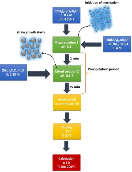
Fig. 2.1 Process block diagram of Al-doped zinc oxide nanoparticles synthesis ... 40
Fig. 2.2 SPS equipment: Dr. Sinter 2080 unit (SPS Syntex Inc., Japan) ... 42
Fig. 2.3 SPS chamber setup and sintering process ... 42
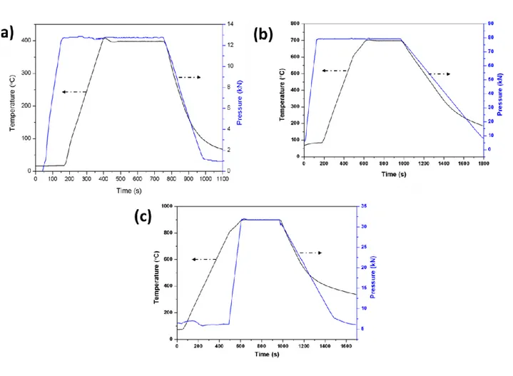
Fig. 2.4 SPS sintering cycles: (a) SC1 for 8mm die (b) SC1 for 20mm and (c) SC2 ... 45
Fig. 2.5 Schematic diagram of the SPS column: (a) Normal setup (b) Current isolation using alumina (c) Sample preparation with alumina ... 45
Fig. 2.6 Photo of ZEM-3 (Ulvac-Riko). ... 49
Fig. 2.7 Illustration of measurement section ... 50
Fig. 2.8 Schematic diagram of LFA 457 MicroFlash (NETZSCH)[199] ... 51
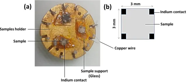
Fig. 2.9 Sample preparation for the physical property measurement: (a) Sample holder (b) arrangement of indium contacts on sample ... 52
Fig. 2.10. Typical example of direct band gap estimation using ZnS film [202]... 53
Fig. 3.1 SEM micrograph (a) of commercial zinc oxide powder and corresponding particle size distribution (b) ... 58
Fig. 3.2 XRD patterns of zinc oxide powder ... 58
Fig. 3.3 Effect of drying ZnO powder: (a) FTIR and (b) Thermo-gravimetric analysis of commercial ZnO powder ... 59
Fig. 3.4 Thermal behaviour of ZnO ceramics in air and vacuum atmospheres ... 60
Fig. 3.5 Relative density and grain size as a function of pressure for ceramics prepared from commercial ZnO powder (T= 400°C) ... 62
Fig. 3.6 XRD patterns of ZnO ceramics sintered at varying pressure... 63
Fig. 3.7 SEM micrograph of fractured surface of ceramics prepared from commercial ZnO powder at various pressures (T = 400 °C) ... 63
Fig. 3.8 Relative density and grain size of ceramics prepared from commercial ZnO as a function of temperature (P = 250 MPa) ... 64
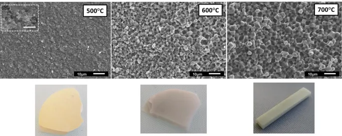
xiii Fig. 3.9 SEM micrographs of fractured surfaces and pictures of as-sintered ceramics showing the effect of sintering temperature... 65 Fig. 3.10 (a) SEM micrograph of fractured surfaces (b) grain size distribution of ceramics prepared from commercial ZnO powder for 8 mm and 20 mm die ... 66 Fig. 3.11 (a) SEM micrograph of fractured surfaces (b) grain size distribution (Image J) of ceramics prepared from ZnO powder (700°C - 250 MPa) ... 67 Fig. 3.12 (a) SEM micrograph of fractured surfaces (b) grain size distribution (Image J) of ceramics prepared from ZnO powder (900°C - 100 MPa) ... 68 Fig. 3.13 Influence of SPS parameters on the densification and grain size of ZnO ceramics (Note: RT is room temperature and HT is holding temperature) ... 69 Fig. 4.1 Characterization of the precipitate (a) XRD patterns and (b) SEM micrographs of zinc oxalate hydrate ... 75 Fig. 4.2 Differential Thermal and Thermogravimetric Analysis of zinc oxalate hydrate. ... 75 Fig. 4.3 XRD patterns of commercial zinc oxide powder and synthetic one, heat-treated at various temperatures (a) and Zoomed 101 peak (b) ... 76 Fig. 4.4 SEM micrographs of synthetic ZnO powders obtained at various calcination temperatures ... 76 Fig. 4.5 Particle size distribution of ZnO powders (ImageJ) ... 77 Fig. 4.6 FTIR (a) and Thermogravimetric analysis (b) of the different ZnO powders ... 79 Fig. 4.7 Displacement ratio and displacement during heating of pure commercial and synthetic ZnO powder in air (700°C) ... 81 Fig. 4.8 SEM micrograph of fractured surfaces and grain size distribution (Image J) (a) CSP ceramic (b) CCP ceramic (700°C-250 MPa)... 83 Fig. 4.9 Displacement ratio and displacement during heating of pure commercial and synthetic ZnO powder in air (900°C) ... 84 Fig. 4.10 SEM micrograph of fractured surfaces and grain size distribution (Image J) (a) CSP ceramics (b) CCP ceramic (900°C -100 MPa-SC2) ... 85 Fig. 4.11 Photographs of (a) CSP ceramic (b) CCP ceramic (900°C -100 MPa-SC2) ... 86 Fig. 4.12 XRD patterns of ZnO ceramics from synthesized powder sintered at 600°C ... 87 Fig. 4.13 SEM micrograph of fractured surfaces of ZnO ceramics prepared from synthesized powder (P=250 MPa) ... 87 Fig. 4.14 Photos of as-sintered ZnO ceramics prepared from synthesized powder ... 88
xiv
Fig. 4.15 Thermogravimetric (TGA) analysis of as-sintered CCP ceramic ... 89
Fig. 4.16 SEM micrographs of as-sintered and annealed CCP ceramic... 89
Fig. 4.17 Resistivity vs Temperature of as-sintered pure ZnO ceramics ... 91
Fig. 4.18 Seebeck Coefficient vs Temperature of as-sintered pure ZnO ceramics ... 93
Fig. 4.19 Thermal conductivity vs Temperature of as-sintered pure ZnO ceramics: (a) resistivity (b) Seebeck Coefficient (c) thermal conductivity (d) power factor (e) ZT ... 95
Fig. 4.20 Performance of as-sintered pure ZnO ceramics with temperature: power factor (a) ZT (b) ... 96
Fig. 4.21 Thermoelectric properties of annealed 900°C-Vacuum-CSP ceramic: (a) resistivity (b) Seebeck Coefficient (c) thermal conductivity (d) ZT ... 97
Fig. 5.1 XRD patterns of pure and Al-doped ZnO oxalate powder ... 102
Fig. 5.2 SEM images of pure and Al-doped ZnO oxalate powder ... 102
Fig. 5.3Thermogravimetric analysis of pure and Al-doped ZnO powder ... 102
Fig. 5.4 XRD patterns of pure and Al-doped ZnO powder ... 103
Fig. 5.5 SEM micrographs of pure and Al-doped ZnO powder ... 104
Fig. 5.6 Particle size distribution of pure and Al-doped ZnO powder ... 104
Fig. 5.7Sintering behavior of pure ZnO and Al-doped ZnO using spark plasma sintering ... 106
Fig. 5.8 Relative density versus temperature of Al-doped ZnO ceramics ... 108
Fig. 5.9 XRD patterns of Al-doped ZnO ceramics at varying temperature ... 109
Fig. 5.10 SEM micrographs of 0 at% and 2 at% Al ZnO ceramic sintered at 700°C ... 110
Fig. 5.11 SEM micrograph of Al-doped ZnO ceramic at different sintering temperatures ... 111
Fig. 5.12 XRD patterns of Al-doped ZnO ceramics sintered at 600C and 650C with a pressure of 250 MPa using RT and HT mode ... 112
Fig. 5.13 XRD patterns of Al-doped ZnO ceramics sintered at 250 MPa and 500 MPa with a temperature of 600°C using HT mode ... 113
Fig. 5.14 SEM micrograph of Al-doped ZnO ceramics sintered at 650°C (HT) and 700°C (RT) ... 114
Fig. 5.15 SEM micrograph of annealed Al-doped ZnO ceramics sintered at 650°C (HT) .... 114
Fig. 5.16 Resistivity versus temperature for annealed pure and Al-doped ZnO ceramics sintered at 650°C (HT) ... 115
Fig. 5.17 Seebeck Coefficient versus temperature for annealed pure and Al-doped ZnO ceramics sintered at 650°C (HT) ... 116
xv Fig. 5.18 Thermal conductivity versus temperature of annealed pure and Al-doped ZnO
ceramics sintered at 650°C (HT) ... 117
Fig. 6.1 XRD patterns of polyaniline emeraldine powder ... 124
Fig. 6.2 SEM micrographs of polyaniline emeraldine powder before (a) and after (b) addition of HCl. ... 124
Fig. 6.3 FTIR spectrum of polyaniline powders with inserted table of resistivity at room temperature ... 125
Fig. 6.4 Thermogravimetric analysis of polyaniline powder before and after acid activation ... 126
Fig. 6.5 XRD patterns of Al-doped ZnO powders and PANI composites. ... 127
Fig. 6.6 SEM micrographs of Al-doped ZnO powders doped with polyaniline powder ... 127
Fig. 6.7 FTIR spectrum of Al-doped ZnO powders doped with polyaniline powder ... 128
Fig. 6.8 Thermogravimetric analysis Al-doped ZnO powders doped with polyaniline powder ... 129
Fig. 6.9 XRD patterns of pure ZnO, ZnA, ZnA-5PANI and ZnA-ZA9PANI ceramics ... 132
Fig. 6.10 SEM micrographs of ZnA, ZnA-0,75PANI ZnA-5PANI and ZnA-ZA9PANI ceramics ... 132
Fig. 6.11 TEM micrographs of ZnA-ZA9PANI ceramic ... 133
Fig. 6.12 Raman spectrum of ZnA and ZnA-5PANI ceramics and PANI pellet ... 134
Fig. 6.13 Thermal conductivity of ZnO, ZnA, ZnA-5PANI and ZnA-ZA9PANI ceramics .. 135
Fig. 6.14 Illustration of thermal vibrations of ZnA-ZA9PANI ceramic at the interface[150] ... 135
Fig. 6.15 Resistivity of ZnO, ZnA, ZnA-5PANI and ZnA-ZA9PANI ceramics ... 136
Fig. 6.16 Arrhenius plot of ZnA-5PANI and ZnA-9PANI ... 137
Fig. 6.17 Seebeck Coefficient of Al-doped ZnO/PANI ceramics ... 138
Fig. 6.18 Performance of Al-doped ZnO/PANI ceramics: (a) Power factor (b) Figure of merit ... 139
xvi
List of symbols
Symbol
Definition
Units
S Seebeck Coefficient V/K, µV/K V Voltage V G, q Conductance S/m f Fermi energy T Temperature K, °C t time s,min E Fermi level eV q Conductance S/m n Carrier concentration m-3
m* Carrier effective mass Kg/g
m mass Kg/g h Planck’s constant m2kg/s ZT Figure of merit e electrons k Thermal conductivity W/m.K L Lorentz number WΩ/K2 Ndc Density of defect - H Enthalpy J Cp Heat capacity J/kg PF Power factor W/m.K2
xvii
kB Boltzmann constant J/K
d Crystallite size M
d, ρ density kg/m3
Q Heat flow W/m2
B Magnetic induction Tesla
I Current A
x thickness M
hv Energy of photons V
R Reflectance -
TE Thermoelectric -
CSP Ceramic prepared from synthetic powder -
CCP Ceramic prepared from commercial powder -
PANI Polyaniline -
SPS Spark plasma sintering -
Com-ZnO Commercial zinc oxide -
XRD Xray-diffractometer -
SEM Scanning Electron Microscopy -
EDX Energy Dispersive X-Ray Spectroscopy -
TEM Transmission electron microscopy -
FTIR Fourier Transform-Infrared Spectroscopy -
BET Brunauer–Emmett–Teller technique -
xviii
TGA thermogravimetric analysis -
ICP-AES inductively coupled plasma atomic emission spectroscopy
-
ICP-OES inductively coupled plasma optical emission spectroscopy
-
Greek Symbol
Symbol
Definition
Units
Δ Change/difference -
µ Carrier charge mobility m2/V.s
ρ Resistivity Ω.m, Ω.cm / g.m-3 α Diffusivity Absorption coefficient m2/s cm-1 σ Electrical conductivity S/m, S/cm π Relaxation time η efficiency %
1
2
General introduction
The global warming due to fossil fuels and the escalating worldwide demand for energy is driving wide investigation and development of sustainable and alternative energy sources. Thermoelectric (TE) devices are considered as an attractive option and are being used for direct conversion of heat to electricity. They are being preferred because of the lack of moving parts, their robustness in harsh environment and also there is no need for high temperature fluids. Currently, the limitations in both heat transfer efficiency and cost of the thermoelectric devices has relegated their application especially for large-scale energy-conversion processes.
At present, much research is focused on improving and developing new thermoelectric materials that are environmentally friendly and inexpensive i.e. containing earth–abundant elements. Hence, the use of metal oxide as TE materials has been thoroughly studied over the past years as green technology materials. In this study, ZnO was chosen because of its high Seebeck Coefficient and carrier mobility which are perfect parameters towards improving thermoelectric performance. However, the main challenge with pure ZnO is the high thermal conductivity and resistivity which reduces the thermoelectric efficiency. Hence, the present study focuses on improving the thermoelectric properties of ZnO by evaluating the processing of ZnO powder and dense ceramics; and also doping and/or incorporation with other materials with an aim to address the mentioned shortfalls.
From literature it was observed that pure ZnO is mostly doped with Group III elements (Al, Ga, In, and B) as source of charge carriers to improve its electrical conductivity. Recently, hybrid structures and nanocomposites are receiving a lot of attention due to the unique properties they possess such as reduction in thermal conductivity. Conducting polymers (such as polythionates, polypropylene, polyaniline, polyacetylene, polypyrrole and polyethylene) are being merged with inorganic composites to create hybrid thermoelectric materials. Polymers have become of interest because they have low thermal conductivity.
The aim of this study was to investigate the dispersion of polyaniline (PANI) in Al-doped ZnO ceramics in order to improve thermoelectric properties of the ceramics prepared through spark plasma sintering (SPS). The successful completion of this project will open new opportunities and important insights on how to produce promising low temperature power generation and cooling systems that can be applied in remote areas. About over a billion
3 people have no access to electricity, hence, the development of off grid solar energy based technologies will transform lives and also benefit those who are currently not being supplied with adequate electricity.
To achieve this noble goal, low cost and manufacturability of polymers are required, as they can be scalable for large applications. This was work focused on understanding the characteristics of synthesized pure and Al-doped ZnO particles and their thermoelectric performance. At first a determination of efficient spark plasma sintering parameters for pure ZnO, Al-doped ZnO and Al-doped ZnO/PANI ceramics was done. This was in order to produce ceramics with preserved nanostructure. Attention was paid on the densification, phase transformation and microstructural evolution. The influence of PANI concentration in Al-doped ZnO ceramics on thermoelectric properties was evaluated.
This thesis is made up of six chapters; Chapter One contains theoretical background on thermoelectricity and literature review on state-of-the-art thermoelectric materials, performance of ZnO based ceramics and hybrid/metal oxide ceramics on their thermoelectric properties. The materials and methods used for the experiment are contained in Chapter two. Chapter three discusses the influence of spark plasma sintering parameters on pure ZnO. The study of ZnO powder quality and spark plasma sintering parameters on thermoelectric properties are discussed in Chapter four. Chapter five contains synthesis, sintering and thermoelectric properties of Al-doped ZnO. Chapter six focuses on the incorporation of polyaniline in the Al-doped ZnO ceramic, the powder preparation, densification and thermoelectric properties are discussed. Conclusions drawn from this study and recommendations made are presented in the last part.
4
Chapter 1
Bibliography
5
1. Bibliography
This chapter provides extensive literature review on current status of thermoelectric materials. The first section focuses on the basic principles of thermoelectricity and the state-of-the-art of thermoelectric materials. Recent progress of promising n-type and p-type metal oxide thermoelectric materials is reviewed. This includes compilation of important parameters such as resistivity, Seebeck Coefficient and thermal conductivity. In-depth discussion on ZnO based thermoelectric materials is presented. The influence of material properties and underlying transport mechanisms are highlighted. Then, a review on thermoelectric properties of ZnO based polymer composites is discussed. Low temperature sintering mechanism of ZnO composites are also discussed in this chapter. Brief conclusions and outlook for future studies are presented.
1.1 Thermoelectricity fundamentals
1.1.1 Thermoelectric effects (Seebeck and Peltier effect)
As highlighted in general introduction, thermoelectricity is a physical phenomenon that occurs in a conductor or semiconductor when exposed to temperature difference or when current is passed through it. There are three thermoelectric effects that occur in materials: Seebeck, Peltier and Thomson effects [1-5]. Thomson effect is the absorption or evolution of heat when current is passed through unequally heated conductor. Seebeck effect is the flow of current due to temperature gradient between two ends of a material. Peltier effect is an inverse of Seebeck effect; it involves heating or cooling of a material on one side when current is passed through it. The description of Seebeck (power generation mode) and Peltier effect (Refrigeration mode) phenomenon is indicated in Fig.1.1. The thermocouples consist of n-type and p-n-type materials for both the power generation and refrigeration mode. When there is a heat source a temperature difference occurs between the two semiconducting/conducting materials. As a result, an open circuit voltage called Seebeck Voltage is produced that causes the bulb to glow (Fig.1.1). Whereas, when current is passed through the semiconducting/conducting junctions it is converted into heat on one end of the material while the other end gets cooler, this process is known as Peltier effect. Fig. 1.1 illustrates cooling as a result of the Peltier effect. There is interdependence between electric current and temperature difference between the hot and cold ends. In this thesis, we will only focus on Seebeck effect.
6 Fig. 1.1Comparison between Seebeck and Peltier effect [5]
A detailed description of Seebeck effect is given in Fig.1.2. A temperature difference causes charge carriers at hot side to become more active and therefore diffuse to the cold side and then accumulate there (Fig.1.2. (a)), until an internal electrical field (E) is built up that depress further migration (Fig.1.2. (b))[6]. The ratio of the voltage developed to the temperature difference (∆V/∆T) is known as Seebeck Coefficient (S) or thermo-power [2, 6, 7]. If the dominant charge carriers in the material are electrons, the electric field will be opposite to the temperature gradient. Hence, the Seebeck Coefficient will bear a negative sign for electrons (n-type). The reverse is true for holes, a positive sign (p-type) is assigned for Seebeck coefficient [2, 6, 7].
Fig. 1.2.Illustration of Seebeck effect [6]: Migration of charge carriers from hot to cold side on n- and p-type (a) and the building up of internal electric field (b).
7 The Seebeck Coefficient can be explained from the first principles of Boltzmann’s kinetic theory that relates it with thermal conductance [8, 9], see Eq. 1.1-1.3.
𝑆 = −∆𝑉
∆𝑇 = − 𝐺𝑠
𝐺 [1.1]
Where G is intrinsic thermal conductance (S/m) and Gs is thermal contact conductance
(S/m), ΔV is change in voltage and ΔT is change in temperature The conductance can be further expressed as follows:
𝐺 = ∫ 𝑑𝐸 [−𝜕𝑓𝜕𝑇] [𝐺(𝐸)] [1.2]
𝐺𝑠 = ∫ 𝑑𝐸 [−𝜕𝑓𝜕𝑇] [𝐺(𝐸)]𝐸−𝜇
𝑞𝑇 [1.3]
Where E is Energy level (eV), f is Fermi function, T is temperature (K), q is conductance (S/m) and µ is mobility (m2/V.s).
Eq. 1.3 shows that the magnitude and sign of Seebeck Coefficient relies on the electronic structure or Fermi function of material [2]. The Fermi energy can be further expressed in terms of effective mass and carrier concentration as shown in Eq. 1.4.
𝐸 = ħ2
2𝑚∗[3𝜋
2𝑛]23 [1.4]
Where h is Planck’s constant (m2
kg/s), m* is carrier effective mass (kg), n is carrier concentration (m-3) and π is pi (3.142).
From the above arguments it follows that a simplified Seebeck Coefficient equation for bulk semiconducting materials is expressed in Eq.1.5 [10].
𝑆𝑏𝑢𝑙𝑘 = 8𝑚∗𝜋2𝑘𝑏2 3𝑒ℎ2 𝑇 ( 𝜋 3𝑛) 2 3 [1.5]
Where Sbulk is Seebeck Coefficient of a bulk material, kB is Boltzmann constant (J/K)
and π is pi (3.142).
It is evident from Equation 1.5 that for high Seebeck Coefficient a large effective mass is required. This explains the high Seebeck Coefficient found in transition metal oxides such as ZnO, MnO2 etc. [11-13]. It is also predicted that by manipulating the temperature and carrier
8 1.1.2 Performance of thermoelectric materials
Thermoelectric materials are constructed into devices that consist of modules for application purposes. The setup is illustrated in figure 1.3; the top part is the thermoelectric device and the bottom enlarged part is the thermocouple. The thermoelectric device is made of thermoelectric couples that consist of a pair of n and p-type thermoelectric elements connected electrically in series and thermally in parallel. Other parts that make up the device are the substrates for heat adsorption and metal interconnects to contact current. In this study we will only focus on the performance of n-type materials.
Fig. 1.3 Typical example of thermoelectric module[14]
The conversion efficiency of a thermoelectric generator is determined from the Carnot efficiency:
ΔT
𝑇𝐻= (𝑇𝐻− 𝑇𝐶)/𝑇𝐻) [1.6]
And reduction factor that takes into account the materials performance (ZT) [2, 5].
𝜂 = [𝑇𝐻−𝑇𝐶 𝑇𝐻 ] [ √1+𝑍𝑇𝑎𝑣𝑒−1 √1+𝑍𝑇𝑎𝑣𝑒−(𝑇𝐶 𝑇𝐻) ] [1.7]
9 Where η is conversion efficiency (%), T is temperature on Hot (H) and Cold side (C) (K), and ZTave is average figure of merit from each thermoelectric couple.
A dimensionless figure of merit (ZT) is a central parameter in characterizing the thermoelectric properties of a material; it is determined by the electrical and thermal transport properties of a material (see Eq. 1.8) [5]. It is shown in Eq.1.8 that large power factor (S2σ or S2/ρ) is desired for high figure of merit while maintaining minimal thermal conductivity. Hence, high figure of merit (ZT) can be attained by materials that exhibit high Seebeck Coefficient and electrical conductivity with very low thermal conductivity. It can be seen that the parameters are interrelated and that makes the enhancement of ZT difficult to obtain.
𝑍𝑇 =𝑆2𝜎𝑇
𝑘 = 𝑆2𝑇
𝜌𝑘 [1.8]
Where k is thermal conductivity (W/m.K), T is temperature (K), S is Seebeck Coefficient or thermo-power (V/K), σ is electrical conductivity (S/m) and ρ is resistivity
(Ω.m).
Different energy conversion technologies and their power generation efficiencies with temperature are given in Fig.1.4. It is presented that improving the ZT value could expand the increasing application of thermoelectric materials. Thermoelectric (TE) materials with ZT > 1 are regarded as high-performance materials with potential to be commercialized [1, 15]. The first application of thermoelectricity was in flight space navigation satellites for radioisotope thermoelectric generators (RTGs) carried out by Thor-DM21 Able-Star in 1961 [16]. RTGs have recently been successfully used in deep-space probes launched by NASA for Cassini missions. Nowadays, thermoelectric devices are being installed in vehicles to recover automobile exhaust heat into useful electrical energy and thereby improving fuel efficiency [1, 17]. Solid state refrigerating devices that uses thermoelectric or Peltier effect have been widely used in computers, infrared detectors and optoelectronic devices for cooling [7, 18]. Thermoelectric car seat climate control system are being commercialized [17]. Recent advances include TE-solar hybrid systems for energy conversion and power generation [15].
10 Fig. 1.4Power generation efficiency versus temperature for different energy conversion technologies [15] (Note: org-Organic, CSP-concentrated solar power, PV- photovoltaic, TE-
thermoelectric, TI-Thermionic)
Highest ZT recorded to date is from Cu2Se and single crystal SnSe (ZT is ~2.6) [19, 20],
though the mission of the thermoelectric community is to reach ZTs values greater than 3 for large scale application [15]. Hence processing routes and new materials are being explored to improve the performance of thermoelectric materials. However, due to the complexity of thermoelectric materials, only few successful researches have been reported, especially for semiconducting metal oxides and polymers. Therefore, better understanding of the thermoelectric concept is required for altering the parameters.
The relationship between ZT and thermoelectric parameters with carrier concentration is given in Fig 1.5. It is shown that there should be a balance of the carrier concentration with Seebeck Coefficient and electrical conductivity to have improved ZT. The trade-off between electrical conductivity and Seebeck Coefficient can also be understood from the electronic density of states. The electrical conductivity of bulk semiconductors is related to charge carrier concentration (n) and mobility (µ) as shown in Eq. 1.9 [5, 10]. There is a clash amongst the parameters looking into Eq.1.5 and 1.9; high carrier concentration will result in high electrical conductivity whereas a decrease in the Seebeck Coefficient will occur. Also, large effective mass is favored for high Seebeck Coefficient while for the electrical conductivity is not the case. Therefore, a trade-off needs to be done amongst these parameters for increasing the ZT value.
11 𝜎 = 𝑛(𝐸)𝑒𝜇(𝐸) = 𝑛(𝐸)𝑒2 𝜋(𝐸)
𝑚∗ [1.9]
Fig. 1.5Figure of merit and behavior of thermoelectric parameters at varying carrier concentration [21]
Thermal conductivity also plays an important role when improving thermoelectric performance. Based on the previous successful researches a minimal thermal conductivity of less than 5 W/m.K is required [20, 22]. Fundamentally, both phonons and electronic charge carriers (electrons or holes) are responsible for thermal transport. The corresponding contributions of these are lattice (l) and electronic (e) thermal conductivity (Eq.1.10 and 1.11)[10].
𝑘 = 𝑘𝑙+ 𝑘𝑒 [1.10]
𝑘𝑒 = 𝐿𝑇𝑛𝑒𝜇 [1.11]
Where L is Lorentz number (2.4 x 10⁻⁸ WΩ/K2)
At high carrier concentration (n >1020 cm-3), thermal conductivity is increased whereas high electrical conductivity is favored as shown in Fig. 1.5. Several studies have been conducted in order to reduce lattice thermal conductivity by phonon scattering through various ways such as nano-structuring [14, 23-27], material doping [10, 28-30] and morphology manipulation using process techniques such as Spark plasma sintering or microwave sintering etc… [24,
12 31-34]. In addition to the above other methods such as the creation of nanopores [35, 36], the elaboration of nanoprecipitates [33, 34, 37] and development of complex structures such as skutterudites [38, 39], clathrates[38, 40], half-heusler [38, 41] etc have been reported for reducing the lattice thermal conductivity. Furthermore, Hicks and Dresselhaus [42] proposed that quantum confinement of charge carriers could increase the power factor, thus improving the ZT. A typical example of how thermal conductivity reduction can enhance the figure of merit is illustrated in Fig. 1.6. Thermal conductivities 0.2 W/mK and 0.8 W/m.K are compared; it could be seen that reducing the thermal conductivity to 0.2 W/mK improves the ZT by two-folds. Reduction in thermal conductivity reduces carrier mobility, as electron scattering will be increased, this will result in high Seebeck Coefficient.
Thus far, nano-structuring has been reported as the most efficient and easier method for reducing the lattice thermal conductivity [14, 23, 43]. The effect of grain size on the thermal conductivity as a function of temperature is given in Fig.1.7 for nano-grained Ga-ZnO ceramics. It is shown that thermal conductivity decreases as the grain size is decreased. Also, as the temperature is increased the thermal conductivity is further reduced. A nanostructured material reduces the phonon mean free path and also offers different phonon scattering modes that could reduce the thermal conductivity. The scattering mechanism that occurs in a nanostructured material is illustrated in Fig.1.8. Mid/Long phonon wavelengths are scattered at the nanoparticles and grain boundaries whereas the short wavelengths are scattered by the atomic defects. At high temperatures the mean free path is decreased due to molecular vibrations. In this work, we will explore the reduction of thermal conductivity by addition of conducting polymers in a transition metal oxide.
13 Fig. 1.6Effect of thermal conductivity on the figure of merit [14]
Fig. 1.7Effect of grain size on thermal conductivity as a function of temperature on nano-grained Ga-ZnO ceramics [44]
14 Fig. 1.8Scattering mechanism of phonons within a nanostructured material [27]
1.2 Current state-of-the-art thermoelectric materials
Previously we have indicated the importance of improving the figure of merit for large scale application and the need to optimize thermoelectric parameters. ZT has been improved enormously over the past decades through intense experimental procedures [1, 45] and theoretical studies on different materials [42, 46, 47]. ZT of different n and p-type thermoelectric materials as a function of temperature are given in Fig.1.9. The classical materials: Bi2Te3[48, 49], PbTe [50-53] and GeSi [54-56] are well known for room
temperature (~300K), mid (300-700K) and high temperature (>700K) applications, respectively. Through band engineering and nano-structuring ZT over 2 was achieved for Na doped SnSe [57], AgSbTe1.85Se0.15[58], Ge0.89SbIn0.01Te[59], Na-doped PbTe-SrTe [60] and
PbTe–PbS [61] composites (Fig 1.9 (a,b)). Over the years, new materials with unique characteristics (such as the Skutterites (MX3, where M is transition metals and X is
Phosphorus, Arsenic, Antimony etc..) [62, 63], Clathrate[64], half-heusler [65] etc…) to improve ZT value have been proposed and studied (Fig1.9 (c))[38]. The highest reported ZT to date for bulk materials is 2.66 at 923K from SnSe single crystal measured along the b axis [19, 45] and recently from indium doped Cu2Se with ZT of 2.6 at 850K [20, 45]. However,
the setback of these materials is the restriction for large scale application as their compounds are made up of rare earth (very expensive) and toxic elements. It is vital to use materials which are abundant and environmentally friendly. Hence, metal oxides are the ideal and most recently studied materials since they are made up oxygen and earth friendly elements.
15 Fig. 1.9Recent advances of different thermoelectric materials: n-type materials[22] (a), p-type
materials [22] (b) and n & p-type of recent thermoelectric materials [66] (c)
1.3 Metal oxide thermoelectric materials
Metal oxides are of interest recently as eco-friendly thermoelectric materials because they are less toxic, inexpensive and have high thermal stability[13]. Thermoelectric devices made from metal oxides are more durable because of their stability in oxidizing environment unlike tellurium, antimony and germanium based compounds. Their electrical properties can be transitioned from insulator to metallic behavior through manipulation of crystal structure, doping/co-doping and chemical compositions [10, 67, 68]. The recent progress on the performance of n-type and p-type metal oxides, in terms of figure of merit vs temperature is given in Fig.1.10. The most promising thermoelectric metal oxides are the p-type layered cobaltite (Ca3Co4O9 and NaxCoO2)[13]. A single crystal Ca3Co4O9+δ was reported to give ZT
16 lutetium gave maximum ZT of 0.61 at 1118K due to drastically reduced thermal conductivity <1.8W/m.K and enhanced thermopower (~240µV/K) induced by Ag nano-inclusions [70, 71]. While, undoped NaxCoO2 with Na/Co ratio of 0.85 showed ZT of 0.78 at 950K [72], and after
doping with silver, the ZT was increased to 0.91 at 950K. Recent advances on the p-type metal oxides are focused on BiCuSeO oxyselides [73]; pristine BiCuSeO has high Seebeck Coefficient of between 300 and 400µV/K at 300-900K with minimal thermal conductivity [29, 68, 73]. As a result, BiCuSeO doped with BaO gave ZT of 1.4 at 900K.
Fig. 1.10 Recent progress on thermoelectric properties of metal oxides. ZT versus temperature for (Bi0.875Ba0.125CuSeO[29], Ca2.7Ag0.3CoO9/10wt%Ag [71], Ca2.8Ag0.05Lu0.15Co4O9+δ[70], Na1.7Co2O4[72], Na1.7Co2O4/10wt%Ag [72], Ca0.9(Dy,Yb)0.1MnO3 [74], Ca0.9Bi0.1MnO3 [75],
CaMn0.98Nb0.02O3 [76], In1.9Ga0.1O3 [77], SrNb0.15Ti0.85O3/3wt% KTO [78], La0.08Dy0.12Sr0.8TiO3 [79], Zn 0.96Al0.02Ga0.02O[28])
The most investigated n-type metal oxides are the perovskite-type such as the strontium titanate (SrTiO3 (STO) and calcium manganite (CaMnO3 (CMO))) [10, 13]. The doping
process of these materials is promoted by creating an oxygen deficient ceramic [68]. An STO doped with potassium titanate (KTO) and lanthanum-doped barium titanate has shown promising ZT values of about 0.38 at 900K [78, 79]. However, the issue with STO is the easy oxidation of Ti3+ ions to Ti4+ ions above 650K [13, 80]; oxygen easily diffuses causing the ceramic to be insulating [81]. Thus, CMO are used for high temperatures greater than 1000K due to stability of Mn3+ ions at these conditions [82]. Unfortunately, its performance has been poor with ZT below 0.2 when doped with bismuth [75] and co-doping with ytterbium and
17 dysprosium [74]. A slight improvement in the ZT of the CMOs was observed doping with Niobium on the manganese site [76]. Other reported work on the thermoelectricity of metal oxides includes gallium doping in indium oxide ceramics [77]; ZT of 0.37 at 1000K was achieved. In this work we will focus on zinc oxide (ZnO), a promising n-type metal oxide with better performances at high temperature. Maximum ZT of 0.65 was reported at 1247K on a dually doped with aluminum and gallium[28]. This will be discussed in details in section 1.4.2.
1.4 ZnO based thermoelectric materials
1.4.1 Characteristics and challenges of pure ZnOZinc Oxide is an n-type semiconductor with a wide band gap between 3.2 to 3.5eV, hence, has broad applications in optoelectronics, piezoelectric, thermoelectricity, gas sensing and photovoltaic due to its unique chemical and physical properties [83-89]. It has good photo-stability, high chemical and thermal photo-stability, high bond energy and broad range of radiation absorption capabilities. Zn metal has high electronegativity which results in less polarized Zn-O bonds. Crystal structures of ZnZn-O are presented in Fig.1.11. At ambient conditions, ZnZn-O normally crystallizes into a thermodynamically stable phase, hexagonal wurzite structure, space group P63mc (Hermann–Mauguin notation) or C6v4 (Schoenflies notation)with lattice
parameters: a = b=3.2488Å, c = 5.2054Å [90]. Depending on the synthesis conditions other crystal structures can be formed; this includes cubic zinc-blende (tetrahedral, formed at high pressures (>9GPa)) and rocksalt (which is mostly formed at very high pressures) [91, 92].
Fig. 1.11Crystal structures of ZnO [92]
Because of the simple crystal structure and light elemental composition, wurzite ZnO struggles from high thermal conductivity which can go as high as ~100 W/m.K at room temperature [93-95] and ~11W/m.K at 1000K [95].This is a setback for the performance of thermoelectric materials. Hence, it is important to find new/upgrade existing processing
18 methods (including powder synthesis and sintering techniques) and explore different dopants to reduce the thermal conductivity. Even though ZnO is praised for its high Seebeck Coefficient of about 600µV/K at room temperature [95], it struggles from low electrical conductivities. Fully annealed sputtered ZnO ceramic with a thickness of 100 nm has resistivity of 104 Ω.cm at room temperature [96]. By introducing dopants and manipulating the stoichiometry of ZnO the resistivity could be reduced towards a metallic behavior, with resistivity ranging between 102-10-3 Ω.cm [83, 91, 97].
1.4.2 Challenges with preparing nanostructured pure ZnO ceramics
As alluded earlier numerous research studies have been reported on the nanostructuring of thermoelectric materials for improving the ZT by thermal conductivity reduction [23, 26, 27, 42]. Different powder synthesis and sintering techniques have been considered for the reduction of grain size. So, nanometric ZnO powders of varying particle size distribution and grain morphology have been synthesized by chemical precipitation, sol gel, emulsion, hydrothermal and microwave techniques [83, 89]. Though, the challenge in consolidating nanopowder ceramics is obtaining full densification and maintaining the nanostructure. Sintering methods such as microwave and spark plasma sintering have been reported for densifying materials while maintaining the nanostructure [98-100]. Because of the high surface area of nanopowders, grain growth rapidly predominates during sintering due to the diffusion of grain boundaries and Ostwald ripening [101-105]. Therefore, it is crucial to be cautious about sintering techniques to minimize grain size. Spark plasma sintering (SPS) is a recent effective sintering technique for consolidating all kinds of materials. It uses rapid heating and high thermal efficiency, and as a result, it contributes to full densification of materials within minutes with retained nano/microstructure [100, 106, 107].
Retaining the nanostructure of ZnO ceramics can result in lower thermal conductivity to about 10 W/mK at room temperature [31, 32]. Usually thermal conductivity of about 35-55W/m.K is reported at room temperature because of the micrometre grain sizes [32, 108-111]. The summary of thermoelectric properties of pure ZnO ceramics at 700 K is presented in Table.1.1. Great progress has been done over the past 2 decades in improving the thermoelectric properties of ZnO ceramics. Advancement in the processing techniques resulted in a decrease in the sintering temperature to less than 400°C which caused a decrease in the grain size from ~30 µm to less than 10 µm [31, 108, 111, 112]. As a result, thermal conductivities of about 12 W/m.K were obtained for fully dense ZnO ceramics. Porosity has been reported as a way to reduce thermal conductivity, however, it has a huge impact on electrical conductivity of ceramics [113]. Virtudazo et al. [32] made a macro/nanoporous ZnO
19 ceramic from nanoporous ZnO powders prepared through double emulsion; lowest thermal conductivity of 4 W/m.K was reported at 700 K due to shortening of phonon mean free path [114]. Thus, ZT of 0.03 was reported for 0.05 Ω.cm of resistivity and -279 µV/K in Seebeck Coefficient, for ZnO ceramic obtained by spark plasma sintering at 550°C. When ZnO ceramic was spark plasma sintered at 950°C, the highest ZT of 0.06 was obtained when the resistivity was 0.002 Ω.cm, and the Seebeck Coefficient of -123 µV/K and thermal conductivity was 11 W/mK. Sintering at high temperature resulted in higher concentration of oxygen vacancies that improved the electrical conductivity of the ceramic, hence, the higher ZT. The theoretical background of ZnO intrinsic defects is discussed in section 1.4.3.
Recently, Cramer et al. [31] reported on the densification of ZnO nanoparticles using modified graphite mould using and spark plasma sintering to enhance thermoelectric properties through simultaneous improvement of Seebeck Coefficicient, electrical conductivity and thermal conductivity through grain size gradation across the ceramic. Relative density of 97% was obtained. The SEM micrograph of the functionally graded material (FGM) is depicted in Fig. 1.12. The grain sizes decreased from the hot to the cold side; 1200 nm to 200 nm. At room temperature the thermal conductivity was 20 W/m.K and 12W/m.K at 700K. It is noticed that the thermal conductivities are in the same range as that of normal sintering at high temperatures. Thermal conductivities of less than 5 W/m.K are required for improvement of the ZT value. The absolute Seebeck Coefficient and resistivity were 180 µV/K and 0.02 Ω.cm at 700K, respectively, which resulted in a ZT of 0.01.
Lowering the sintering temperature could be used to reduce the thermal conductivity by causing little or no grain growth. There have been reports about sintering of ZnO nanoparticles at low temperatures, less than 600°C [115-118]. Ceramic grain sizes of about 200 nm resulted in reduced thermal conductivity of about 10 W/m.K at room temperature. Unfortunately, this caused an increase in the resistivity to ~80 Ω.cm because of scattering of electrons at the grain boundaries and reduction in crystallinity [31]. ZnO being a non-stoichiometric semiconductor, it is easily affected by temperature and sintering atmosphere which has a huge influence on the resistivity. These last points will be discussed in detail in section 1.4.3.
20 Table 1.1 Thermoelectric properties of pure ZnO ceramics at 700K
Yr. Technique Sintering conditions Powder crystallite size Ceramic grain size RD ρ S k PF ZT Ref. nm µm % Ω.cm µV/K W/m.K 10-4W/m.K2 2017 SPS Differential sintering, 73MPa, 773-1173K 18 (Nanoparticle) 0.18-1.2 97 0.02 -180 12 1.43 0.01 [31] 2017 SPS 3.5kN, Argon 20 (Nanoporous) [32] 823K <10 78 0.05 -279 4 1.73 0.03 1023K ~5-25 80 0.006 -195 12 6.79 0.04 1223K ~5-30 91 0.002 -123 11 9.53 0.06 2016 SPS 125MPa, Vacuum, 1173K - (Nanoparticle) - (Annealed) >98 3.64 -600 20 0.1 3.5x10 -4 [95] 2015 SPS Argon 1173K 13.8 (Nanoparticle) 1-2 93 0.13 -300 12 0.68 3.9x10 -3 [111] 2013 SPS 1173K ~70 0.1-1 (Annealed) - 0.3 -374 15 0.47 2.2x10⁻³ [109] ~100 (Nanoparticle) - 4 - 6 - -
2011 Hot press Air 1673K 28 (Nanoparticle) 31 >97 1.25 -280 14 0.06 3.1x10 -4 [108] 2005 SPS Vacuum 1273K - (Nanoparticle) <10 99 251 -500 11 0.001 6.3x10⁻⁶ [112]
1997 Hot press Air 1673K
-
(Nanoparticle) - 99 0.1 -325 18 1.06 4.1x10
21 Fig. 1.12SEM micrographs of functionally graded ZnO ceramic[31]
1.4.3 Intrinsic ZnO defects
Even though ZnO is praised for its high Seebeck Coefficient value ranging between 300-600µV/K thanks to the use of SPS technique depending on the concentration of charge carriers, which are controlled by powder synthesis methods, sintering techniques and annealing procedures, it still suffers from low electrical conductivities as highlighted in the previous sections [95, 109, 110, 112]. Through doping and manipulation of stoichiometry of ZnO ceramics the resistivity could be reduced towards metallic behavior. The defects in pristine ZnO play an important role in the electrical properties [91, 119-121]; by controlling operating parameters such as the sintering atmosphere, temperature etc… the concentration of defects could be tuned. There are different defects which can form within the ZnO bandgap. The ionization energy of the defects is shown in Fig. 1.13 [119] : zinc interstitials (Zni) close
to the conduction band with energies between 0.05-0.15 eV, oxygen vacancies (VO) with
energies between 0.05-2 eV and zinc vacancies (VZn) close to the valence band with energies
22 Fig. 1.13Ionisation energy of ZnO point defects at room temperature [119]
The defects chemistry in ZnO using the Kroger vink notation is presented in Eq. 1.12-1.19, based on the Frenkel and Schottky reactions [119].
Frenkel defect formation reactions: Zinc Interstitials
𝑍𝑛𝑍𝑛 ↔ 𝑍𝑛𝑖𝑋+ 𝑉𝑍𝑛𝑋 [1.12]
𝑍𝑛𝑖𝑋 ↔ 𝑍𝑛𝑖⦁+ 𝑒− [1.13]
𝑍𝑛𝑖⦁↔ 𝑍𝑛𝑖⦁⦁+ 𝑒− [1.14]
Schottky defect formation reactions: Oxygen vacancies
𝑂 ↔ 𝑉𝑍𝑛𝑋 + 𝑉𝑂𝑋 [1.15] 𝑉𝑂𝑋 ↔ 𝑉𝑂⦁+ 𝑒− [1.16] 𝑉𝑂⦁↔ 𝑉𝑂⦁⦁+ 𝑒− [1.17] Zinc vacancies 𝑉𝑍𝑛𝑋 ↔ 𝑉𝑍𝑛, + ℎ⦁ [1.18] 𝑉𝑍𝑛, ↔ 𝑉𝑂,, + ℎ⦁ [1.19]
Where i is interstitial site, Zn is zinc, O is oxygen, V is vacancy, e- is electron, h is hole and the superscripted are the charges (a prime indicates negative charge, a dot a positive charge
and cross indicates anion site)
The zinc interstitials (Zni) always donate 2+charge electrons to the conduction band in a
23 partially filled in their energy orbitals, they can accept additional electrons, and are known to be deep acceptors because of the high transition levels of 0.18-0.87 eV. Oxygen vacancies (VO) are deep donors with high formation energy, also known to be responsible for the n-type
conductivity in ZnO. Whereas, the oxygen interstitials (Oi) can be split into two and acts as a
deep acceptor in n-type ZnO and could react with the lattice to form covalent bonds with host oxygen that could be a donor.
The possibility of a defect to contribute to conductivity is determined through the density of defects (Nde) in Eq.1.20 [122]. Nde depends on the enthalpy of defect formation. The
relationship between enthalpy and atomic radius is that, the bigger the atomic radius the higher the enthalpy of defect formation (ΔH) which leads to low Nde based on the relationship
between ΔH and Nde (Eq. 1.20). Oxygen and zinc have Van der Waals radius of 152 and 142
pm [123], respectively. Thus, oxygen will have higher ΔH and low Nde, and zinc will have
low ΔH and higher Nde. This implies that the most vital contributing defects on the
conductivity of ZnO are the zinc interstitials and vacancies. Since, zinc interstitials have the lowest energy level compared to zinc vacancies it is the main contributor giving the n-type conductivity in native ZnO.
𝑁𝑑𝑒 ∝ exp[−
∆𝐻
𝑘𝐵𝑇] [1.20]
Where Nde is the density of defect, H is the enthalpy of defect formation (J), kB the
Boltzmann constant (J/K) and T the temperature (K).
It was previously highlighted that the formation and concentration of ZnO defects depends on the operational parameters. ZnO defects are sensitive to processing atmosphere; Fig.1.14 relates the concentration of ZnO defects with oxygen partial pressure. It is revealed that at low partial pressure of oxygen (reducing atmosphere) the concentration of oxygen vacancies predominates. In stoichiometric conditions, the concentration of oxygen vacancies equals that of oxygen interstitials which is rare for polycrystalline ZnO. The conductivity could be tuned from n-type to p-type depending on the partial pressure of oxygen.
24 Fig. 1.14Concentration of ZnO defects as a function of oxygen partial pressure at room
temperature [124]
On the electrical properties, the influence of the sintering parameters on the resistivity and Seebeck Coefficient of pure ZnO ceramics are shown in Table.1. The resistivity and Seebeck Coefficient vary between 0.002 to 251 Ω.cm and -123 to 600µV/K, respectively; depending on the grain size, relative density and concentration of oxygen vacancies. High power factor (σS2
) of 9.53 x10⁻⁴ W/m.K2 was achieved with low resistivity of 0.002 Ω.cm and Seebeck Coefficient of -123µV/K, whereas ceramics with high Seebeck coefficients of -600 µV/K and resistivity of 3.64 gave low power factors of about 3.5x10⁻⁴ W/m.K2. Therefore, it is vital to have very high electrical conductivities for better performance while maintaining the Seebeck Coefficient at moderate level. Several research studies have been done on the addition of substitutional dopants on the zinc side to narrow the band gap with the objective to obtain higher electrical conductivities [125].
1.4.4 Doped and co-doped ZnO TE properties
Zinc oxide is usually doped with the group III elements as they have ionic radius close to that of Zn2+ ions (0.074 nm) [126, 127]. The ionic radius of aluminium (Al3+), indium (In3+) and gallium (Ga3+) ions are 0.054, 0.080 and 0.062 nm respectively. These elements act as shallow donors substituting some part of the zinc side giving carrier concentrations higher than1020 cm-3 [83]. The recent progress of ZnO based thermoelectric ceramics are given in Fig.1.15. There are several reports on thermoelectric properties of Al-doped ZnO with ZTs
![Fig. 1.5 Figure of merit and behavior of thermoelectric parameters at varying carrier concentration [21]](https://thumb-eu.123doks.com/thumbv2/123doknet/2150597.9236/29.892.223.678.102.573/figure-merit-behavior-thermoelectric-parameters-varying-carrier-concentration.webp)
![Fig. 1.10 Recent progress on thermoelectric properties of metal oxides. ZT versus temperature for (Bi 0.875 Ba 0.125 CuSeO[29], Ca 2.7 Ag 0.3 CoO 9 /10wt%Ag [71], Ca 2.8 Ag 0.05 Lu 0.15 Co 4 O 9+δ[70] , Na 1.7 Co 2 O 4 [72], Na 1.7 Co 2 O 4 /10wt%Ag [72], Ca 0.9 (Dy,Yb) 0.1 MnO 3 [74], Ca 0.9 Bi 0.1 MnO 3 [75],](https://thumb-eu.123doks.com/thumbv2/123doknet/2150597.9236/34.892.107.828.341.675/recent-progress-thermoelectric-properties-oxides-versus-temperature-cuseo.webp)
![Fig. 1.20 Thermoelectric properties of AZO and PANI at room temperature [177] 1.4.7 Low temperature sintering of ZnO based ceramics](https://thumb-eu.123doks.com/thumbv2/123doknet/2150597.9236/52.892.184.659.214.532/thermoelectric-properties-pani-temperature-temperature-sintering-based-ceramics.webp)
![Fig. 2.10. Typical example of direct band gap estimation using ZnS film [202]](https://thumb-eu.123doks.com/thumbv2/123doknet/2150597.9236/71.892.253.629.645.1034/fig-typical-example-direct-band-estimation-using-zns.webp)