HAL Id: tel-01835620
https://tel.archives-ouvertes.fr/tel-01835620
Submitted on 11 Jul 2018HAL is a multi-disciplinary open access archive for the deposit and dissemination of sci-entific research documents, whether they are pub-lished or not. The documents may come from teaching and research institutions in France or abroad, or from public or private research centers.
L’archive ouverte pluridisciplinaire HAL, est destinée au dépôt et à la diffusion de documents scientifiques de niveau recherche, publiés ou non, émanant des établissements d’enseignement et de recherche français ou étrangers, des laboratoires publics ou privés.
region using InGaN pseudo substrate for monolithic
white LED application
Armelle Even
To cite this version:
Armelle Even. In incorporation improvement in InGaN based active region using InGaN pseudo substrate for monolithic white LED application. Optics [physics.optics]. Université Grenoble Alpes, 2018. English. �NNT : 2018GREAY008�. �tel-01835620�
THÈSE
Pour obtenir le grade de
DOCTEUR DE LA COMMUNAUTE UNIVERSITE
GRENOBLE ALPES
Spécialité : PHYSIQUE DES MATERIAUX
Arrêté ministériel : 25 mai 2016
Présentée par
Armelle Even
Thèse dirigée par Ivan-Christophe Robin, et encadrée par Amélie Dussaigne
préparée au sein du Laboratoire d’Electronique et de Technologie de l’Information (LETI-CEA)
dans l'École Doctorale de Physique
Amélioration de l'incorporation d'indium dans zone
active à base d'InGaN grâce à la croissance sur
pseudo-substrat InGaN pour l'application à la DEL
blanche monolithique
In incorporation improvement in InGaN based
active region using InGaN pseudo substrate for
monolithic white LED application
Thèse soutenue publiquement le 27 février 2018 devant le jury composé de :
Monsieur Nicolas Grandjean
Professeur, EPFL-LASPE, Rapporteur, Président
Monsieur Pierre Lefebvre
Directeur de recherche, CNRS-L2C, Rapporteur
Monsieur Henri Mariette
Directeur de recherche émérite, CNRS-NPSC, Examinateur
Monsieur Adrian Avramescu
Expert de haut niveau, OSRAM Opto Semiconductors GmbH, Examinateur
Monsieur David Sotta
Ingénieur-Chercheur, Soitec, Invité
Monsieur Ivan-Christophe Robin
Ingénieur-Chercheur, Aledia, Directeur de thèse
Madame Amélie Dussaigne
Voici venu le temps des remerciements. Je tiens à exprimer ma reconnaissance envers toutes les personnes que j’ai croisées pendant ces trois années et qui ont rendu la réussite de cette thèse possible.
Cette thèse a été préparée au sein du laboratoire LMP au CEA-Leti. Je remercie Alain Millon pour m’avoir accueilli dans son laboratoire ainsi qu’Anne Roule qui a pris sa suite. Merci pour votre intérêt pour le sujet et d’avoir fait en sorte que cette thèse se déroule dans les meilleures conditions. Merci également à Bernard André pour l’accueil dans son service et pour les nombreux moyens mis à disposition.
En premier lieu, je remercie Amélie Dussaigne mon encadrante pour ses conseils avi-sés, son soutien sans faille et pour m’avoir appris à être plus autonome aussi. Ce fut un plaisir de travailler avec toi pendant ces trois années.
Merci à Ivan-Christophe Robin mon directeur de thèse pour ses suggestions et ses relec-tures du manuscrit. Merci pour m’avoir initié à la simulation, pour tes nombreuses idées et les échanges toujours très intéressants.
Je tiens à remercier tout particulièrement l’équipe de MOCVD du M23 dans laquelle je me suis sentie bien pendant ces trois années.
Je remercie Mathieu Lafossas pour m’avoir initié à la MOCVD et avoir partagé son expé-rience et ses connaissances sur l’équipement. Cette thèse n’aurait pas été possible sans un équipement en parfait état. Merci à Rémy Obrecht puis à Frédéric Barbier pour l’avoir assisté. Merci aussi pour les discussions sur les XRD et les couches "partiellement relaxées" et pour avoir partagé avec moi le suspens du lundi matin pour savoir si la RSM de 56 heures n’avait pas planté pendant le week-end ! Merci à vous trois pour vos coups de main quand j’en avais besoin.
Un grand merci à Pierre Ferret pour son initiation à la diffraction aux rayons X des ni-trures. Merci également pour les nombreuses discussions passionnantes sur tout un tas de sujets (sur la thèse mais pas que) et pour m’avoir fait me poser les bonnes questions et prendre un peu de recul quand cela était nécessaire.
Je remercie également mes collègues doctorants Gautier Laval et Timotée Journot pour avoir été de très bonne compagnie pendant cette thèse. Merci à Gautier pour m’avoir bien accueilli dans l’équipe, pour avoir répondu à mes questions et pour avoir toujours veillé à ce que l’équipe ne m’oublie pas pour aller manger malgré mon exil au D6 ! Merci à Timotée pour les bavardages dans le bureau, je te souhaite courage pour la rédaction ! Merci aussi à Sofia Boughaleb et Benjamin Samuel qui ont fait leur stage dans l’équipe et continuent en thèse. Je vous souhaite plein de réussite dans votre thèse et bon courage aussi.
Je remercie la team du LMP D6 pour m’avoir accueilli dans leur couloir, Dominique Giotta, Jean-Louis Santailler et les autres. Merci pour votre bonne humeur constante tout au long de ces trois années. Une pensée particulière pour Aymeric Tuaz mon co-bureau, merci de m’avoir supporté et pour la compagnie quand toutes les lumières du couloir étaient depuis longtemps éteintes ! Merci à toutes les autres personnes du LMP, Béran-gère Hyot, Carole Pernel et les autres. Un remerciement particulier à Roselyne Templier pour son initiation au MEB et sa bonne humeur.
Une pensée pour François Levy, merci pour avoir fait le lien entre l’équipe et Soitec. Merci également pour tes précieux conseils, relectures et pour ta compagnie en conférence (on se souviendra longtemps de l’ouragan et des 24 h coincés à l’hôtel à Orlando !).
Je remercie l’équipe qui a réalisé le processing de mes LEDs en salle blanche du D6, un merci particulier à Helge Haas pour avoir été toujours disponible pour répondre à mes questions sur la techno. Du côté d’Aledia, merci à Michael Delalande pour les nombreux coups de mains sur la PL du M23 et à Florian Dupont pour avoir accepté de prendre les vendredis comme jours de manips ce qui a bien arrangé toute l’équipe !
Je voudrais également remercier toutes les personnes avec qui j’ai collaboré à la PFNC. Merci à Adeline Grenier pour ses analyses de sonde atomique et pour sa disponibilité pour m’en expliquer les principaux ressorts. Un remerciement à David Cooper pour ses ana-lyses d’holographie électronique et ses explications. Je tiens également à remercier Névine Rochat pour ses analyses de cathodoluminescence et pour m’avoir initié à cette technique de caractérisation. Merci aussi à Christophe Licitra pour la formation et l’aide sur le mon-tage de micro-photoluminescence. Merci également à Eric Robin pour ses caractérisations EDX et à Denis Mariolle pour m’avoir formé à l’utilisation de l’AFM.
J’adresse mes remerciements à l’équipe de la ligne ID01 à l’ESRF. Merci à Tobias Schulli, à Carsten Richter pour ses analyses détaillées, à Marie-Ingrid Richard et à Yves-Matthieu Le Vaillant pour avoir fait le lien entre Soitec, l’ESRF et le CEA-Leti.
Merci à l’entreprise Soitec et aux personnes impliquées dans le projet InGaNOS pour avoir accepté de nous faire parvenir les substrats InGaNOS qui ont permis d’obtenir ces
résul-Je remercie également les rapporteurs de ce manuscrit, Nicolas Grandjean et Pierre Le-febvre ainsi que Henri Mariette et Adrian Avramescu pour avoir accepté de faire partie de ce jury et pour l’interêt qu’ils ont porté à cette thèse.
Merci aux amis de Grenoble et d’ailleurs pour leur amitié tout au long de ces trois an-nées. Je remercie mes parents pour m’avoir donné le goût aux sciences et pour leur soutien pendant la durée de cette thèse mais également tout au long de mes études supérieures. Merci aussi à mes soeurs, Morgane et Blandine.
List of acronyms 1
Introduction 5
1 Growth of InGaN alloy 9
1.1 Properties of AlInGaN system . . . 9
1.1.1 Structural properties . . . 9
1.1.1.1 Crystallography . . . 9
1.1.1.2 Polarity . . . 11
1.1.2 Electronic and electric properties . . . 11
1.1.2.1 Spontaneous polarization . . . 11
1.1.2.2 InGaN bandgap energy . . . 12
1.2 InGaN alloy . . . 13
1.2.1 Indium miscibility in GaN . . . 13
1.2.2 InGaN growth conditions- MOVPE and MBE . . . 13
1.2.2.1 MetalOrganic Vapor Phase Epitaxy (MOVPE) . . . 13
1.2.2.2 Molecular Beam Epitaxy (MBE) . . . 14
1.2.3 Nature of InGaN alloy . . . 14
1.2.3.1 Indium inhomogeneities . . . 14
1.2.3.2 Carrier localization in InGaN . . . 15
1.2.3.3 Indium clustering . . . 16
1.2.3.4 Origin of carrier localization . . . 18
1.3 Heteroepitaxy of InGaN on GaN . . . 18
1.3.1 Lattice mismatch and biaxial strain . . . 19
1.3.1.1 Lattice mismatch . . . 19
1.3.1.2 Biaxial strain . . . 20
1.3.1.3 Critical thickness . . . 21
1.3.1.4 2D-3D Transition . . . 24
1.3.1.5 Dependance of bandgap on strain . . . 24
1.3.2.1 Point defects . . . 25
1.3.2.2 Dislocations . . . 25
1.3.2.3 V-pits . . . 26
1.3.3 Piezoelectric polarization and Quantum Confined Stark Effect . . . 27
1.3.3.1 Piezoelectric polarization . . . 27
1.3.3.2 Internal electric field . . . 28
1.3.3.3 Quantum Confined Stark Effect (QCSE . . . 29
1.3.4 Strain and In incorporation . . . 30
1.3.4.1 Effect of strain on indium miscibility . . . 30
1.3.4.2 Compositional pulling effect . . . 30
1.3.4.3 In segregation . . . 31
1.4 Quantification of indium in InGaN . . . 33
1.4.1 Rutherford Back Scattering spectrometry (RBS) . . . 33
1.4.2 Atomic Probe Tomography (APT) . . . 35
1.4.3 Energy-dispersive X-ray spectroscopy (EDX) . . . 36
1.4.4 Secondary Ion Mass Spectrometry (SIMS) . . . 37
1.4.5 Photoluminescence (PL) . . . 38
1.4.6 Cathodoluminescence (CL) . . . 40
1.4.7 High Resolution X-Ray Diffraction (HRXRD) . . . 41
1.4.8 Conclusion . . . 43
Conclusion . . . 44
2 White and color LEDs 53 2.1 White LEDs . . . 53
2.1.1 Colorimetry . . . 53
2.1.2 Different types of white lights . . . 55
2.1.2.1 Non LEDs sources of white light . . . 55
2.1.2.2 White LEDs . . . 57
2.1.3 White monolithic LEDs : Principles and raising issues . . . 59
2.1.3.1 Principle . . . 59
2.1.3.2 Issues . . . 59
2.1.4 White monolithic LEDs : Simulation on carrier distribution with indium in the barriers . . . 62
2.2 The green gap . . . 65
2.2.1 Reasons for the green gap . . . 67
2.2.2 Solving the green gap . . . 70
2.2.3 Our approach to bridge the green gap . . . 75
2.2.3.1 Previous attempts . . . 76
Conclusion . . . 78
3 Towards greater wavelengths on GaN 87 3.1 Limitations of the regular structure on GaN . . . 87
3.1.1 Influence of TMIn flux . . . 87
3.1.2 Influence of growth pressure . . . 88
3.2 InGaN layers on GaN . . . 90
3.2.1 Growth conditions . . . 90
3.2.2 Surface quality assessment . . . 92
3.2.3 Influence of growth rate . . . 93
3.2.3.1 Optical and surface characterization . . . 93
3.2.3.2 PL vs T . . . 94
3.3 MQWs on SL and prestrained layers . . . 97
3.3.1 PL and IQE measurements . . . 97
3.3.2 Investigation of the reasons for the IQE improvment . . . 99
3.4 Reduction of indium surface segregation . . . 103
3.4.1 First interface . . . 103
3.4.2 Second interface . . . 107
Conclusion . . . 110
4 Growth of InGaN layers on InGaNOS substrates 115 4.1 InGaNOS substrates . . . 115
4.1.1 Fabrication process . . . 116
4.1.2 Donors . . . 117
4.1.3 InGaNOS substrates . . . 119
4.2 Regrowth of InGaN layers on InGaNOS . . . 123
4.2.1 Influence of substrate on emission wavelength and In content . . . . 124
4.2.2 Assessment of the quality of the layers . . . 127
4.2.3 PL behavior with temperature . . . 129
4.2.4 Insertion of GaN interlayers . . . 130
4.2.5 Variation of the growth temperature . . . 133
4.3 ESRF experiment . . . 136
4.3.1 Description of the experiment . . . 136
4.3.2 Results . . . 138
Conclusion . . . 140
5 InGaNmultiple quantum wells on InGaNOS substrates 143 5.1 Growth of full InGaN structures on InGaNOS substrates . . . 143
5.1.1 Influence of substrate on emission wavelength . . . 144
5.1.3 MQW sample characterizations . . . 150
5.1.3.1 Crystal quality . . . 150
5.1.3.2 Visualization of the V-defects . . . 151
5.1.3.3 Surface quality assesment . . . 152
5.1.3.4 Cathodoluminescence characterization . . . 154
5.2 Fine characterizations of the green MQWs on InGaNOS . . . 156
5.2.1 Quantum well width . . . 156
5.2.2 Quantification of indium content in the MQWs . . . 157
5.2.2.1 XRD measurements . . . 158
5.2.2.2 EDX . . . 158
5.2.2.3 APT . . . 159
5.2.3 Determination of electric field by electron holography . . . 162
5.2.3.1 Principle . . . 162
5.2.3.2 Results . . . 163
5.2.4 IQE measurements and PL behavior with temperature . . . 165
5.2.4.1 PL spectra behavior with temperature . . . 165
5.2.4.2 Internal Quantum Efficiency . . . 168
5.2.4.3 Best IQE achieved and comparison with literature . . . 170
5.3 LED structures . . . 171
5.3.1 n-InGaN and p-GaN layers . . . 171
5.3.2 LED structure emitting at 510 nm . . . 173
5.3.2.1 Optical characteristics . . . 174
5.3.2.2 Processing details . . . 174
5.3.2.3 Caracterization after processing . . . 175
5.3.3 Remaining challenges . . . 176
5.3.3.1 Current spreading . . . 177
5.3.3.2 p-doping . . . 177
Conclusion . . . 178
General conclusion and perspectives 183 A XRD 187 A.1 XRD Principle . . . 187
A.2 Different types of measurements . . . 188
A.3 What can be obtained from the different scans . . . 189
A.3.1 ω scan-Rocking Curve (RC) . . . 189
A.3.2 Reciprocal Space Mapping (RSM) . . . 189
A.3.3 2θ − ω . . . 191
A.5 Determination of the strain and the indium content for an InGaN on GaN
layer from the a and c lattice parameters . . . 193
A.5.1 First case : pseudomorphic growth . . . 193
A.5.2 Second case : non pseudomorphic growth . . . 193
B Photoluminescence (PL) 197 B.1 What information can be obtained with PL measurements . . . 197
B.2 Experimental set-up . . . 198
B.3 Choice of experimental conditions . . . 199
B.3.1 Choice of the laser . . . 199
B.3.2 Choice of the measurement temperature . . . 200
B.4 IQE measurements . . . 200
B.4.1 Procedure . . . 200
B.4.2 Hypothesis . . . 201
C Other characterization techniques 205 C.1 Notion of standard . . . 205
C.2 Atomic Force Microscopy (AFM) . . . 205
C.3 Cathodoluminescence (CL) . . . 206
C.4 Atom Probe Tomography (APT) . . . 207
C.5 Transmission Electron Microscope (TEM) . . . 208
C.6 Energy Dispersive X-ray (EDX) . . . 208
C.7 Rutherford Backscattering Spectrometry (RBS) . . . 208
C.8 Secondary Ion Mass Spectroscopy (SIMS) . . . 208
C.9 Transmission Line Measurements (TLM) . . . 209
D French Summary 213 D.1 Introduction . . . 213
D.2 L’alliage InGaN . . . 214
D.3 LEDs blanches et LEDs de couleur . . . 215
D.4 Vers de plus grandes longueurs d’ondes sur GaN . . . 217
D.5 Croissance de couches InGaN sur substrats InGaNOS . . . 217
D.6 Puits quantiques sur substrats InGaNOS . . . 218
AFM Atomic Force Microscopy APT Atome Probe Tomography
CIE Comission Internationale de l’Eclairage CL Cathodoluminescence
CT Color Temperature
CRI Color Rendering Index
ECV Electrochemical Capacitance Voltage EDX Energy Dispersive X-ray spectroscopy EQE External Quantum Efficiency
ESRF European Synchrotron Radiation Facility FWHM Full Width at Half Maximum
HAADF High Angle Annular Dark Field HRXRD High Resolution X-ray Diffraction III-N III Nitrides
IL Interlayer
LED Light Emitting Diode MBE Molecular Beam Epitaxy
MOCVD MetalOrganic Chemical Vapor Deposition MOVPE MetalOrganic Vapor Phase Epitaxy MQW Multiple Quantum Wells
NID Not Intentionally Doped
PAMBE Plasma Assisted Molecular Beam Epitaxy
PL Photoluminescence
PLD Pulsed Layer Deposition
QD Quantum Dot
QB Quantum Barrier
QCSE Quantum Confined Stark Effect
QW Quantum Well
RBS Rutherford Back Scattering spectrometry
RC Rocking Curve
RGB Red Green Blue
RMS Root Mean Square
RSM Reciprocal Space Mapping SAG Selective Area Growth
SIMS Secondary Ion Mass Spectroscopy
SL SuperLattice
SEM Scanning Electron Microscope
STEM Scanning Transmission Electron Microscope TCAD Technology Computer Aided Design
TEM Transmission Electron Microscope TMIn Tri Methyl Indium
UCSB University of California, Santa Barbara
UL Underlying Layer
UV Ultra Violet
XRD X-ray Diffraction WPE Wall Plug Efficiency
The 2014 Physics Nobel Prize was awarded to Isamu Akasaki, Hiroshi Amano and Shuji Nakamura "for the invention of efficient blue light-emitting diodes (LEDs) which
has enabled bright and energy-saving white light sources" based on the InGaN/GaN
ma-terial system. Since the 1970’s, this mama-terial system had been extensively studied but because of the low material quality and the resistivity of the p-type layers, the research was abandoned. Yet, in 1989, Amano et al. [1] succeeded in activating the magnesium dopant in GaN yielding the first p-n junction. Nakamura et al. then fabricated the first blue LED, by inserting InGaN/GaN Quantum Wells (QWs) in the active region in 1994 [2].
Then, with the addition of YAG (Yttrium Aluminum Garnet) phosphors, white light emission was achieved [3]. In comparison to other sources of white light (incandescent light bulb, fluorescent lamp...), white LEDs present several advantages like their long li-fetime and their good luminous efficacy. As a consequence, LED lighting market share is growing and the LED lighting penetration was 22 % in 2017 and is expected to reach up to 63 % in 2022 [4]. Nonetheless, phosphor-based LEDs present some problems related to the phosphor lifetime and stability of emission wavelength with operating temperature (incompatible with a good quality lighting) as well as losses associated with the phosphor-down conversion. Alternatively to this converted approach, the white monolithic LED was introduced in 2001 [5] with an active region composed of blue and yellow emitting QWs. Yet, the efficiency of such LEDs is limited by the low efficiency of the yellow or red emit-ting QWs .
LEDs are also widely used for the display, backlighting and liquid crystal application. However, if LEDs consistuting the blue pixels are manufactured with AlInGaN material system, the material consistuting the LEDs of the red colored pixels is different, the AlIn-GaP material system is employed. For the green (or yellow) pixels, there is no material system which provides efficient LED emission but they are usually AlInGaN based. This problem is reffered to as the "green gap". The integration of the RGB (Red Green Blue) pixels grown with different material systems is also troublesome for micro-displays and the ideal would be to grow the three RGB pixels with III-N.
But, if the III-N based compounds can theoretically cover the whole visible range, their efficiency decreases as the emission wavelength is increased. This phenomenon is partly attributed to the low miscibility of indium in GaN and to the strain between the InGaN QWs of the active region and the GaN on sapphire usually used as the substrate. In addition, the internal electric field which is increased as the QWs are widenned or when indium content is increased furthers hampers the LED efficiency. Furthermore, the strain is also responsible for the compositionnal pulling effect which prevents an easy indium incorporation and therefore limits the emission wavelength. Moreover, the efficiency droop for high carrier injections which is already problematical for blue light emission, is aggra-vated for long wavelength emission.
To tackle the green gap problem with the AlInGaN material system, in this thesis, we propose to grow an LED structure on a relaxed InGaN substrate. Thanks to this process, a higher indium incorporation rate should be observed [6] as well as a reduction of the internal electric field [7]. As InGaN bulk does not exist, the InGaN pseudo-substrates called InGaNOS are used for this study. They are manufactured by Soitec using their Smart Cut technology. On these substrates, a full InGaN structure can be grown. These structures may then be used to fabricate monochromatic LEDs in the green, yellow or even red range for the integration of RGB pixels or high quality lighting. Alternatively, an efficient white monolithic LED can be considered thanks to this growth process.
The first chapter details the specificities of the InGaN alloy. The properties of the InGaN material in its relaxed and strained states are described with a particular focus on the issues related to the growth of InGaN on GaN. Then, an exhaustive review of the characterization techniques to quantify the indium content in InGaN thick layer and InGaN QWs is presented to determine which techniques will be used to characterize the samples in this thesis.
The different types of white LEDs are described in chapter 2. The white monolithic LED suffers from the unbalanced carrier distribution between the different MQWs of the active region and the low efficiency of the green and red QWs. A simulation study that uses In-GaN in the barriers is shown to control the distribution of the carriers. The issues related to the green gap are then reported together with the existing solutions to overcome it. This leads us to unveil our original solution for an efficient LED emitting at long wave-length based on a full InGaN structure on InGaN substrate.
In the third chapter, solutions are studied to reach long wavelengths on GaN on sapphire. First, attempts based on simple variations of the growth parameters show the intrinsic limitations. Structures using thick InGaN or InGaN/GaN superlattices are then studied with a preliminary study of the InGaN layers on GaN. Next, a study to reduce the surface segregation of indium in InGaN/GaN QWs is conducted.
In Chapter 4, the InGaN pseudo-substrates called InGaNOS and their fabrication process are introduced. Then, a detailed study of the InGaN regrown layers on InGaNOS
sub-thanks to experiments done at the European Synchrotron Radiation Facility (ESRF). Subsequently, in Chapter 5, the MQWs grown on InGaNOS substrates and GaN tem-plates are characterized throuroughly. The internal quantum efficiencies measured for these structures are benchmarked to the existing literature. Lastly, the properties of the first LED grown on an InGaNOs substrate are described with a focus on the remaining challenges to achieve efficient emission at long wavelength.
References of the introduction
[1] H. Amano, M. Kito, K. Hiramatsu and I. Akasaki. Jpn. J. Appl. Phy. 28, L2112 (1989).
[2] S. Nakamura, T. Mukai and M. Senoh. Appl. Phy. Lett. 64, 1687 (1994).
[3] K. Bando, K. Sakano, Y. Noguchi and Y. Shimizu. J.of Light & Visual Evt 22, 2 (1998).
[4] J. Wu. Smart Lighting, Niche Lighting and Lighting in Emerging Countries are Top
Three Driving Forces for Global LED Lighting Market Trend. LED Inside (2017).
[5] B. Damilano, N. Grandjean, S. Vézian and J. Massies. J. Cryst. Growth 228, 466 (2001).
[6] Y. Inatomi, Y. Kangawa, T. Ito, T. Suski, Y. Kumagai, K. Kakimoto and A. Koukitu.
Jpn. J. Appl. Phy. 56, 078003 (2017).
1
Growth of InGaN alloy
This first chapter introduces the concepts for the growth of InGaN-based LEDs. First, some of the properties of the AlInGaN material system will be presented. The nature of the InGaN alloy will be particularly detailed. Then, we will focus on the specific growth of InGaN on GaN and its difficulties. We will especially describe the issues related to strain. Finally, a review of the techniques to quantify indium content in InGaN thick layers and in InGaN quantum wells will be presented.
1.1
Properties of AlInGaN system
1.1.1
Structural properties
1.1.1.1 CrystallographyAlInGaN-based semiconductors are compounds formed by the association of atoms from the column III of the periodic table (aluminum, gallium and indium) and nitrogen atom from the column V. Two different crystalline structures can be found : a stable hexa-gonal form called wurtzite and a meta-stable cubic form of zinc-blende type. Cubic form material with good quality remains hard to manufacture because of its thermodynamical instability. Therefore, only wurtzite structures will be studied throughout this thesis.
Figure 1.1 represents the wurtzite unit cell of GaN. The gallium (Ga) and nitrogen (N) atom individually form a sublattice which is of hexagonal type. The Bravais hexagonal unit cell is a prism which has base edges of same length a and desoriented of 120◦. The height of the prism is noted c.
In the three index hexagonal coordinate system (a1, a2, c) associated with this unit cell, Ga
atoms are localized at (0, 0, 0) and (2/3, 1/3, 1/2) and N atoms at (0, 0, u) and (2/3, 1/3, u+ 1/2) with u = 0.378.
We therefore have two hexagonal sub-lattices, one formed by the Ga atoms and the other formed by the N atoms having an offset of 3/8 along c axis. The a and c lattice parameters
of GaN, InN and AlN are given in table 1.1.
Figure 1.1 – Crystalline unit cell of wurtzite GaN [1].
III-N a (Å) c (Å)
GaN [2] 3.1878 5.185
AlN [3] 3.112 4.981
InN [4] 3.538 5.703
Table 1.1 – a and c lattice parameters of wurtzite structure for GaN, AlN and InN.
Usually for the hexagonal cell, the 4 Bravais-Miller indice notation (h, k, i, l) is used with
i = −(h + k) but the (h, k, l) notation is also used. Some of the planes, including
c-planes {0001} perpendicular to c axis and the m-c-planes {1100} parallel to the c axis are represented in Figure 1.2.
Figure 1.2 – Depiction of the plans of the wurtzite structure with their Bravais-Miller notation [1].
1.1.1.2 Polarity
The structure of the wurtzite cell is not centrosymmetric as the dangling bonds at the surface of the material in (0001) and (0001) are not equivalent. As pictured in Fig.1.3, when the Ga atom has three bonds in the direction oppposite to the growth direction, the material is known as Ga-polar. Conversely, when the N atom has three bonds in the growth direction, the material is named N-polar. The (0001) face of the crystal is called Ga-face (noted as +c) and the (0001) face is called N-face and noted as -c.
Figure 1.3 – Ga polarity and N polarity of wurtzite structure of GaN from [5].
1.1.2
Electronic and electric properties
1.1.2.1 Spontaneous polarizationIn the wurtzite structure, the barycenters of negative and positive charges do not coincide. This spatial separation of electrons and holes creates a dipole and gives rise to spontaneous polarization. The spontaneous polarization vector is illustrated in Fig. 1.3. Table 1.2 summarizes the values of spontaneous polarization for AlN, GaN and InN com-piled by Vurgaftman [6] et al..
III-N Psp(C.m−2))
GaN -0.034
AlN -0.090
InN -0.042
For the InGaN alloy, the spontaneous polarization can be expressed with the following formula [7] :
Psp(InGaN ) = x × Psp(InN ) + (1 − x) × Psp(GaN ) − b × x × (1 − x) (1.1)
The recomended value for the bowing parameter b by Vurgaftman [6] et al. is b = 0.037
C.m−2.
1.1.2.2 InGaN bandgap energy
The lattice parameter of III-nitrides ternary alloys can be expressed with the Vegard’s law [8] from the values of the lattice parameters of the the binary compounds presented in 1.1. Vegard’s law can only be applied in the case where we consider completely relaxed material.
aInxGa1−xN = x × aInN + (1 − x) × aGaN (1.2)
cInxGa1−xN = x × cInN + (1 − x) × cGaN (1.3) For the expression of the bandgap energy a third term called the bowing parameter has to be added to the Vegard’s law :
EgInxGa1−xN = x × EgInN + (1 − x) × EgGaN + b × (1 − x) × x (1.4)
The values of the bandgap for the binary compounds are given in Table 1.3 from the review of Vurgaftman et al.[6]. The value given for the bowing parameter of InGaN can vary between 1.4 eV and 2.8 eV depending on the sources and on the In content and InGaN thickness, the value recomended by Vurgaftman et al. for small In contents [6] is 1.4 eV.
III-N Eg (eV)
GaN 3.510
AlN 6.25
InN 0.78
Table 1.3 – Energy bandgaps for GaN, AlN and InN at 0 K in the wurtzite structure from [6].
1.2
InGaN alloy
1.2.1
Indium miscibility in GaN
Because of the difference in size between the Ga atom (covalent radius of 126 pm) and the In atom (covalent radius of 144 pm) and the small binding energy between In and N, the miscibility of In in GaN is very poor. Ho et al. [9] studied the thermodynamics of the bulk InGaN alloy. The phase diagram (Fig. 1.4) they established shows that at the temperatures necessary for InGaN growth (typically between 650˚C and 800˚C), the alloy is unstable over a wide range of compositions (also shown in [10] and [11]).
Typically, when In content is greater than 25 %, phase separation may occur [12]. This has been evidenced in several experimental studies in layers grown by MBE [13] and MOVPE [14].
Figure 1.4 – Phase diagram for the InxGa1−xN alloy. Binodal (solid) and spinodal
(dashed) curves [9].
1.2.2
InGaN growth conditions- MOVPE and MBE
1.2.2.1 MetalOrganic Vapor Phase Epitaxy (MOVPE)
In this thesis, all samples were grown using MetalOrganic Vapor Phase Epitaxy (MOVPE) in an Aixtron Closed-Coupled Showerhead 6x2 inches reactor. In this technique, the growth is conducted in a reactor with cold walls. Only the substrate is heated and main-tained at the desired growth temperature. The gas precursors used for the growth of GaN are trimethylgallium (T M Ga) and ammonia (N H3). For the growth of the InGaN
al-loy, triethylgallium (T EGa) is usually preferred to supply Ga atoms and trimethylindium (T M In) to supply In atoms. The ammonia and the other species (T M In, T M Ga, T EGa) are introduced separately in the reactor in order to avoid any side reaction. The species are either carried by hydrogen (under the H2 form), nitrogen (under the N2 form) and
they will meet at the substrate’s surface. Subjected to heat, they will dissociate by pyroly-sis. Atoms resulting from decomposition are then adsorbed on the substrate’s surface and diffuse until their incorporation or desorption. The chemical residues are then evacuated using the carrier gases. For GaN, the equation of the decomposition is as follows :
Ga + N H3 GaN + 3/2 H2 (1.5)
Typically, GaN growth is conducted around 1000-1100˚C. However, growth of InGaN requires lower temperatures between 650˚C and 800˚C because In atoms desorb at higher temperatures. For InGaN growth, T EGa is preferred to T M Ga to suppply Ga atoms as the breakdown of the molecules constituing the gas occurs at a lower temperature and carbon contamination is reduced. The growth temperature is a key parameter and will be used as a setting parameter to control the incorporation of indium in the layer. While GaN growth rate can be set at a rather high value (about 2.2 µm/h in our case), InGaN growth rate is compelled to be very low (about 0.1 µm/h in our case) because of the low N H3 cracking efficiency at the InGaN growth temperatures. Indeed, N H3 cracking
efficiency decreases with the temperature [15].
To compensate this low cracking efficiency, the flux of N H3 is set at a high value. The
V/III ratio corresponds to the ratio of the flux of N H3over the flux of the others precursors
(T M Ga or T EGa, T M In).
In this thesis, GaN growth was conducted under H2 atmosphere while for InGaN layers,
N2 was preffered.
1.2.2.2 Molecular Beam Epitaxy (MBE)
In case of MBE, lower growth temperatures are needed, usually around 550 ˚C. This low temperature could be a reason explaining the low structural quality of the InGaN/GaN quantums wells (QWs) grown by MBE due to the presence of high point defect density [16]. For a particular type of MBE, the plasma assisted MBE (PAMBE), 100 % of the nitrogen is active. With this technique, the whole range of indium compositions is attainable.
1.2.3
Nature of InGaN alloy
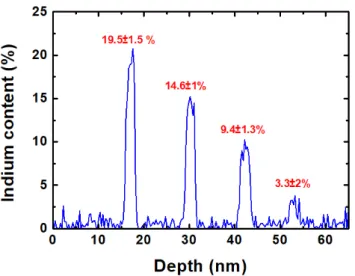
1.2.3.1 Indium inhomogeneitiesBecause of the difficulty to incorporate In in GaN, the InGaN alloy presents an inho-mogeneous distribution. It has been evidenced in samples grown by MOVPE [17], [18], [19], [20],[21], [22] and by MBE [17], [20], [23] and for different growth directions [24], [25]. Fig. 1.5 displays the results of the Atom Probe Tomography (see annex C.4) characteri-zation for two InGaN/GaN quantum wells (QWs) in one of our Multiple Quantum Well (MQW) structures emitting at 500 nm (sample E presented in chapter 5). The position
of indium atoms in the QWs are given by the red dots. The mean In content is measured to be 17.5 %. The isocurves in In composition reveal strong inhomogeneities.
Figure 1.5 – 3D reconstruction of a volume of 20 × 30 × 3 nm3 for an active region of an InGaN/GaN MQW sample and In isocurves for the two first QWs.
1.2.3.2 Carrier localization in InGaN
Figure 1.6 – PL energy vs Temperature for a green emitting InGaN/GaN MQW struc-ture.
Fig. 1.6 shows the evolution with temperature of the central emission energy of the PL spectrum of InGaN/GaN MQW emitting in the green range. This curve follows an "S-shape" and deviates from the Varshni equation [26] which normally governs the evolution of the bandgap energy with temperature. This behavior has been reported in InGaN/GaN MQWs [27], [28] and in InGaN thin films [29], [30], [31], [32]. The phenomenon evidences a temperature-dependant localization of carriers.
The S-shape of the curve may be explained using Fig. 1.7 from [33]. The situation at low temperature is as on Fig. 1.7 (a), all the carriers are distributed randomly on the
different potential minima. When the temperature is increased, the thermal activation allows carriers to diffuse into the deepest potential wells (Fig. 1.7 (b)) which provokes a red-shift of the emission energy. Fig. 1.7 (c) then illustrates the phase of stabilization of emission energy or blue-shift, even the more localized carrier start to be mobile. Finally when the temperature is high enough, thermalization of carrier becomes more and more important (Fig. 1.7 (d)) and the carriers become fully delocalized and the emission energy follows Varshni’s law.
Figure 1.7 – Schematic diagrams indicating the possible mechanism of carrier transfer amongst the potential fluctuations in an MQW structure at different temperatures [33].
1.2.3.3 Indium clustering
Fig 1.8 displays the In distribution in an N-polar InGaN/GaN quantum well analyzed by Atom Probe Tomography (APT). In content presents a strong variation, with regions poor in indium and regions where the indium content reaches up to 30 %. This sample presents indium clustering.
(a) (b)
Figure 1.8 – 2D distribution of In composition in an InGaN/GaN QW (a) Indium fraction profile from the sampling volume displayed on the left (b) (from [25]).
An indium cluster is a region where there is an abnormal high concentration of indium. The presence of indium clusters was reported in some of these references [17], [19], [20], [22]. Jinschek et al. [34] report In contents up to 40 % and cluster sizes of 1-3 nm. Most of these studies use TEM to characterize the samples and visualize the position of In atoms. Yet, beam damage effects have been demonstrated [35]. Therefore, indium clustering evidenced by TEM must be questionned and extreme care should be used when employing this technique. Even data acquired after a minimum time sets an upper limit for inhomogeneity. Humphreys et al. [36] demonstrated that the indium clustering observed on TEM images was the result of beam damage as their APT reconstruction showed that the indium composition was the one of a random alloy. Several other groups observed that their samples showed no sign of indium clusterization [37], [38]. Using TEM below the damage threshold, Baloch et al. also evidenced no clustering in their samples [39]. But clustering does exist in certain cases. Using APT, Tang et al. [40] found evidence of clustering in their QW grown on a-plane orientation while their samples grown on c-plane were cluster-free. In order to assess the presence of clusters, the distribution with the distance to nearest indium atom or the distribution with the In fraction is plotted (see Fig. 1.9). If the distribution follows the binomial distribution, we are in a presence of a random alloy like in the case of the sample on c-plane here. Otherwise, if the distribution deviates from the binomial distribution, there is evidence for indium clustering. Since the reconsideration of the indium clustering, it has been evidenced several times on c-plane [41] and other orientations [25], [40].
Figure 1.9 – Frequency distribution analysis of InGaN/GaN MQW samples grown on a-plane and c-plane from [40]. The c-plane sample on the bottom has a distibution which follows the binomial distribution characteristic of the random alloy while the a-plane sample deviates from that distribution which reveals the presence of indium clustering.
The presence of indium clusters probably depends on the growth conditions of the InGaN layers and the indium content. The reason for this indium clustering is not clear. Since indium clustering is observed in the vicinity of c-screw dislocations, Lei et al. suggested that there is an interaction between these dislocations and the In atoms [42].
1.2.3.4 Origin of carrier localization
There are several hypotheses for the origin of the carrier localization. Since many groups observed indium clustering sometimes to an extent where they could be considered as Quantum Dots (QDs), they believed carriers were localized at these clusters, a theory mentionned for example in [22], [43], [44], [45]. Since the reconsideration of the clustering question, it was shown that localization occured even in samples showing a random alloy distribution [36], [46], [38]. By comparing their model calculation to their experimental observations, Graham et al. proposed that well width fluctuations were responsible for this localization [46]. A difference of one monolayer is already enough to justify a localization energy of 58 meV in their case.
But, these QW width variations are not required to observe the localization of carriers. Indeed, theoretical studies of Bellaiche et al. for InGaN bulk predicted that localization of holes may happen even in layers showing random alloy distribution whereas in the case of InGaAs and AlGaAs, clusters of a few atoms are necessary [47]. Hangleiter et
al. [48] proposed that carriers localize in the vicinity of V-pits (see 1.3.2.3) therefore
preventing them to recombine at the dislocations. The theory was confirmed recently with a detailed cathodoluminescence (CL) study by Massabuau et al. [49]. They attributed this localization to the formation of In-N chains and atomic condensates in the vicinity of dislocations, an opinion shared by Chichibu et al.[50]. We will report in chapter 2 on the beneficial effects of this localization on QW efficiency.
1.3
Heteroepitaxy of InGaN on GaN
III-N substrates of wide diameter with a reasonable price are not widely available. Therefore, homoepitaxy (growth of a material on a substrate of same nature and compo-sition) can rarely be considered. Heteroepitaxy (growth on a material of different nature) of III-N material is a great challenge. Here, we focus on the heteroepitaxy of InGaN on GaN as it is a process encountered during the growth of InGaN-based LEDs. The GaN that serves as a substrate is either bulk GaN known as free-standing (FS) GaN or GaN strained on sapphire substrate.
1.3.1
Lattice mismatch and biaxial strain
1.3.1.1 Lattice mismatch
When a material of in-plane lattice parameter aL is grown on a substrate of in-plane
lattice parameter aS, the in-plane lattice parameter is imposed by the substrate layer.
The lattice mismatch between the layer and the substrate is expressed as follows :
∆a/a = (aL− aS)/aS (1.6)
Two cases may be found. As illustrated in Fig 1.10, when aL < aS the above layer is said
to be under tensile strain. In the case when aL > aS, the layer is under compressive strain.
This is the case of InGaN on GaN.
Figure 1.10 – Schematic representation of the strain of the grown layer (lattice parameter
aC) according to the substrate’s lattice parameter.
The lattice mismatch between InN and GaN is equal to 11%, which foreshadows high lattice mismatch for the growth of InGaN on GaN even for small In contents.
There are cases when the layer is neither fully strained on the substrate nor fully relaxed as if it were bulk material. The relaxation percentage is defined as follows [51] :
R = a meas L − aS arelax L − aS (1.7) with ameas
L , the a lattice parameter of the layer as measured and arelaxL , the a lattice
1.3.1.2 Biaxial strain
As the total volume is maintained, the out-of-plane c parameter will vary as a function of the a lattice parameter. This phenomenon known as biaxial strain is isotropic in the plane and may be described by Hooke’s law in the case of III-N submitted to small deformations.
σ = C.ε (1.8)
σ is the the tensor of stress in the material related to ε, the tensor of strain by C, the tensor
of elastic coefficients. In the case of the wurtzite structure, the tensort C corresponds to a 6 × 6 matrix with 5 independant coefficients.
σxx σyy σzz σxy σyz σzx = c11 c12 c13 0 0 0 c12 c11 c13 0 0 0 c13 c13 c33 0 0 0 0 0 0 c44 0 0 0 0 0 0 c11 0 0 0 0 0 0 1 2(c11− c12) · εxx εyy εzz εxy εyz εzx (1.9)
The relative deformation of the layer is defined from the variation between the value of the lattice parameter (a, c) and their value in the relaxed case (a0, c0). It will be negative
in the case of compressive strain and positive in the case of tensile strain.
εxx = εyy = a − a0 a0 (1.10) εzz = c − c0 c0 (1.11)
If no force is applied to the material, the direction [0001] is not under strain. Therefore, the only components of the strain which are not equal to zero are the ones along the growth plane. Hence :
σzz = 2c13εxx+ c33εzz = 0 (1.12)
The values of elastic constants c13 and c33 may be found in table 1.4. The values for
ternary alloys are determined with a linear interpolation between the values for the binary compounds.
The dependance of deformation along the growth axis on the deformation parallel to the surface is expressed as follows
εzz = −
2 c13
c33
III-N c13(GP a) c33(GP a) GaN 100 [52],104 [53],106 [54],103 [55] 392 [52],376 [53],388 [54],405 [55] AlN 127 [52],112 [53],108 [55] 382 [52],383 [53],373 [55] InN 94 [52], 92 [55] 200 [52],224 [55]
Table 1.4 – Value of elastic coefficients for GaN, AlN and InN.
The factor −2 c13
c33
is known as the biaxial Poisson coefficient. It can be expressed as a function of the isotropic Poisson coefficient ν.
νc= − εzz εxx = 2 c13 c33 = − 2 ν ν − 1 with ν = c13 c13+ c33 (1.14) The value of the Poisson isotropic coefficient is given to be νGaN = 0.183 [56] for MOVPE
GaN and νInN = 0.272 [55] for InN. The value for InGaN at a given composition x can
be linearly interpolated between the values for the end members.
The variation of the in-plane stress is therefore related to the in-plane strain with M the elasticity modulus. σxx = (c11+ c12− 2 c2 13 c33 ) εxx = M εxx (1.15)
The elastic energy is related to the stress and to the strain of the material. For a thin layer, the energy per unit area is expressed as a function of the thickness of the material
h : E´elastic S = 1 2σijεijh = M h ε 2 xx (1.16)
In the case of pseudomorphic growth (when the layer is fully strained) the composition of the layer may be deduced from the measurement of c lattice parameter with the following formula from [51] : x = 1 − ν 1 + ν × cInGaN meas − cGaN0 cInN 0 − cGaN0 (1.17) The values of the c lattice parameters of the binary compounds may be found in table 1.1.
1.3.1.3 Critical thickness
When the layer has a lattice mismatch with the substrate, the plastic energy stored in the layer increases with the thickness of the grown layer. When the layer remains under
the critical thickness hC, the growth is pseudormophic. Then, if a layer is grown above the
critical thickness, metamorphic growth occurs and the layer relaxes through generation of dislocations (see paragraph 1.2.2 on defects).
In the case of InGaN on GaN, the in-plane strain is very large. For instance an In0.1Ga0.9N
layer grown on GaN has an in-plane strain of 1% [57].
Fig. 1.11 gathers data from experimental studies for the growth of InGaN on GaN as well as the theoretical predictions from two models described later (see (a) and (b)). From the experimental data, we expect that for an indium content under 20 %, layers up to 100 nm thickness may be obtained but as soon as the indium content is above 20-25 %, the critical thickness is limited to a few monolayers, which may be critical even for the growth of QW.
The following paragraphs review some theoretical models for the determination of critical thickness applied to growth of InGaN on GaN. For all the models, some of the parameters are dependant on the indium composition noted as x.
Figure 1.11 – Experimental critical thickness of InGaN on GaN dependence on the indium content [58], [59], [60], [61], [62], [63], [64], [65] and theoretical models [66],[67] adapted from [68].
a- Mathews and Blakeslee (Mechanical Equilibrium model) [66] In this theory, misfit is accommodated by generations of a rectangular array of non interacting edge dislocations. hC = b 2πf × 1 − ν(x)cos2α (1 + ν(x))cosλ × (ln hC b + 1) (1.18)
with α angle between the dislocation line and its Burger vector
with λ angle between the glide plane of the dislocation and the interface with b norm of Burger’s vector
b- People and Bean (Energy balance model) [67] In the energy balance model, the critical thickness hC is reached when the areal strain energy density of the layer exceeds
the self-energy necessary for the formation of an isolated screw dislocation at a distance
hC from the free surface.
hC(x) = ( 1 − ν(x) 1 + ν(x)) × ( 1 16π√2) × ( b2 a(x)) × ( 1 f2(x)) × ln( hC(x) b ) (1.19)
with ν(x) Poisson coefficient
with a(x) in-plane lattice parameter with f (x) = ∆a/a lattice mismatch
c- Frank and Van der Merve [69] Van der Merwe was the first to calculate the critical thickness based on energy considerations. We reach the critical thickness when the interfacial energy between the layer and the substrate reaches the minimum energy necessary for the generation of dislocations.
hC = Kb2 4πBε0bedge|| × lnhCED b (1.20) with B = 2µ(1 + ν) 1 − ν
with b||edge the magnitude of the edge component of the Burger’s vector with ε0 native lattice mismatch
with ED energy of the dislocation core
with K = µ 1 − ν
d- Fischer [70] In 1994, Fischer et al. presented a new refined model taking into account the interaction between straight misfit dislocations.
x = bcosλ
0.0836hC
× 1 − (ν(x)/4)
4πcos2λ(1 + ν(x))× ln(hC/b) (1.21)
In Fig. 1.11, one can notice that the experimental critical thicknesses deviate from the theoretical predictions from the energy balance model [67] and mechanical equilibrium model [66] for the high indium contents. This discrepancy may be attributed to a series of factors. As the InGaN alloy has some peculiarities (indium inhomogeneities, high density of dislocations...), the theoretical models may not be adapted to this material . Expe-rimentally, the critical thickness could depend on the growth conditions that are used. Nonetheless, we can see that for very high indium contents like the ones necessary for the
growth of quantum wells for color LEDs, the critical thickness will in any case be limited to only a few nanometers.
1.3.1.4 2D-3D Transition
Several groups report a change in growth mode above a certain thickness [71],[72] in the growth of InGaN on GaN. The growth process may be described by the Fig. 1.12. During the first part, the growth is pseudormorphic, a 2D growth mode is observed and the In content is rather homogeneous. In a second phase, 3D growth starts and the InGaN islands can coherently relax near their top. Then, the tips on the top get more indium-rich while the trenches contain less indium.
Figure 1.12 – Mechanism of InGaN growth on GaN and the 2D-3D transition as proposed by [72].
1.3.1.5 Dependance of bandgap on strain
The behavior of InGaN layers strained on GaN will differ from relaxed InGaN. Orsal
et al. [73] determined the bandgaps of relaxed and strained InGaN layers dependence
on In content from room temperature photoluminescence and cathodoluminescence mea-surements plotted in Fig.1.13. As disclosed above, the bandgap of InN and the bowing
(a) (b)
Figure 1.13 – Low In content dependence of the bandgap emission energy in fully strained (a) and relaxed (b) InGaN layers from [73].
parameter of InGaN can be set to 0.78 eV and 1.4 eV, respectively in the relaxed case at 0 K [6] although many different values may be found in the litterature. Depending on the
sources, at 300 K these values can vary between 0.64 and 0.77 eV. In the strained case, the theory predicts a theoretical increase of 0.1 eV [73] and therefore the InN bandgap is expected to vary between 0.74 and 0.87 eV. For these range of InN bandgaps, the fitting of the curves in Fig. 1.13 gives the bowing parameter dependency in the relaxed and strained case. The bowing parameter may be calculated as [73] :
bstrained = 1.154 × EgInN + 0.396 (1.22)
brelaxed = 1.230 × EgInN + 2.010 (1.23)
1.3.2
Defects in InGaN
When the lattice mismatch between the layer and the substrate is substantial as in the case of InGaN on GaN, structural defects appear.
1.3.2.1 Point defects
There are several types of point defects : — Extra atoms or self interstitials
— Impurities either at interstitial location or substituing for other atoms (oxygen and carbon mostly)
— Missing atoms or vacancies
Point defects appear in InGaN because of the low growth temperature. They will be more numerous in an MBE-grown layer which requires temperatures of about 550˚C compared to an MOVPE-grown layer with temperatures about 750 ˚C.
1.3.2.2 Dislocations
Dislocations may be defined by their unit vector parallel to their propagation direction and their Burgers vector which norm b represents the amplitude of the local deformation of the lattice. There are three types of threading dislocations represented on Fig. 1.14 :
— Screw dislocations also noted c. Their Burgers vector is parallel to unit vector and with the direction <0001>
— Edge dislocations noted c. Their Burgers vector is perpendicular to their unit vector and with the direction <1120>
— Mixed dislocations which have a screw and an edge component with a Burgers vector along a+c and equal to 1/3 <1123>.
Dislocations preferentially move along specific crystallographic planes. A dislocation glide occurs when the dislocation moves in the surface which contains both its unit vector and its Burgers vector. The glide of the dislocation helps to relax the strain in the crystal.
(a) (b)
Figure 1.14 – Direction of the Burgers vector of the wurtzite structure [74] (a) and the different types of dislocations [75] (b).
1.3.2.3 V-pits
Figure 1.15 – Perspective view (a) and cross-section view (b) showing the six sides of the open hexagonal pyramid defined by the {1011} planes [76].
Another very common defect called V-pit or IHP (for Inverted Hexagonal Pyramid) has been evidenced in InGaN-based structures. Fig 1.15 pictures a perspective and a cross section schematic view of a V-pit. At the V-pit apex, a threading dislocation is found. Shiojiri et al.[77] showed that the dislocation forms when the dislocation meets the InGaN QW and propagates to the free surface after the V-pit as can be seen on these TEM images in Fig. 1.16. The V-pit sidewalls are oriented as the {1011} planes.
The formation mechanism has been tentatively explained by several groups. According to Northrup et al. [78], V-pits developp when dislocation cores open up during the growth of the InGaN MQW. It has been observed that a rise in the indium content is related to an enlargment and a multiplication of V-pits. V-pit growth is explained by a reduced incorporation of Ga on the {1011} planes compared to the {0001} surface. Indium atom is suspected to act as a differential surfactant causing this differenciation ([78], [76]). The high growth temperature of GaN (around 1050˚C) as compared to the one necessary for the growth of MQW (typically between 650˚C and 800˚C) explains the fact that these defects are very rarely seen in GaN. The surface diffusion lengths are then high enough to prevent any deviation from a planary growth.
For others [79],[80], [81], [82] the formation of V-pits in InGaN/GaN (0001) is favorable as it is suspected to be one of the principal mechanism for relaxation of strain. According to Song et al. [80] the gliding of dislocations is not possible in InGaN layers because of the low growth temperature. Therefore the strain relief may occur thanks to the V-defects.
(a) (b)
Figure 1.16 – HAADF (High Angle Annular Dark Field)-STEM (Scanning Transmission Electron Microscopy) image of a capped In0.2Ga0.8N (2.5 nm)/GaN (8 nm) MQW layer
grown on a GaN :Si layer (a) Schematic diagram of the structure of the V defect, which nucleates at a threading dislocation in the first In0.2Ga0.8N QW (b) from [77].
1.3.3
Piezoelectric polarization and Quantum Confined Stark
Effect
1.3.3.1 Piezoelectric polarization
Piezoelectricity is a phenomenon ocurring in some materials which, when subject to mechanical stress, acquire electrical polarization. A difference of potential appears as well as electric charges at the surface. As InGaN is grown on GaN, the lattice parameters (a, c) deviate from the nominal ones (a0, c0). Piezoelectric polarization is related to the
relative deformation of the layer εxx and to the elastic (c13,c33) and piezoelectric constants
(e31,e33) :
PP Z = 2εxx× (e31−
e33c13
c33
) (1.24)
We give the values of the piezoelectric constants for AlN, GaN and InN in table 1.5. The elastic constant values may be found in table 1.4.
The magnitude of piezoelectric polarization in InGaN/GaN QW is very large. In this case, spontaneous polarization is negligible compared to piezoelectric polarization [84]. Piezoelectric polarization for InGaN may be expressed as a function of the values for GaN and InN [7]. Unlike spontaneous polarization, piezoelectric polarization follows Vegard’s law without additional term :
III-N e31(C.m−2) e33(C.m−2)
GaN -0.49 0.73
AlN -0.60 1.46
InN -0.57 0.97
Table 1.5 – Value of piezoelectric coefficients for GaN, AlN and InN [83].
1.3.3.2 Internal electric field
For a single QW with quantum barriers (QB), we evaluate the effect of piezoelectric polarization on the internal electric field of the QW for a growth along the c-axis.
The charge surface density at the interface between the QW and the QB is defined as :
σintQW/QB = n(PQB− PQW) (1.26)
PQB and PQW are the total polarization (piezoelectric and spontaneous) at each side of
the interface. n is the vector normal to the (0001) surface.
The vector of the displacement field D = εF + P is conserved between the two materials. The electric field is noted F.
εQWε0FQW − εQBε0FQB = PQB− PQW (1.27)
ε0 is the dieletric constant of vacuum and εQW and εQB are the dielectric constants of the
material of the QW and QB respectively.
We have a continuity of the band structures implying :
tQWFQW + tQBFQB = 0 (1.28)
with tQW and tQB the thciknesses of the QW and the QB respectively. If we express
the internal electric field in the quantum well as a function of polarization, we get the following equation :
FQW =
tQW(PQB− PQW)
εQWε0tQW + εQBε0tQB
(1.29) Lefebvre et al. [85] have experimentally determined the electric field in InGaN/GaN MQW to be around 2.5 M V /cm for an indium content of 20%. For a similar content Bernardini
et al. [86] theoretically calculated a value of 3.3 M V /cm. The differences may be explained
by the fact that the interfaces of the quantum well are not ideal (as detailed in paragraph on indium segregation).
1.3.3.3 Quantum Confined Stark Effect (QCSE
The internal electric field has an influence on the transition energy in the quantum well. This effect is known as the Quantum Confined Stark Effect (QCSE). The funda-mental transition energy in a QW (i.e. between conduction band and heavy hole band) is expressed as follows : :
Ee−hh = e1+ hh1+ EgQW − Ry − eFQWtQW (1.30)
e1 and hh1 are the electron and hole energy levels in the well ; respectively. EgQW is the
energy of the bandgap of the material constituing the well and Ry is the excitonic Rydberg
energy (exciton binding energy). The term −eFQWtQW accounts for the influence of the
internal electric field. As a consequence, the transition energy is lowered compared to a square QW [87]. The red-shift in the emission wavelength gets bigger all the more as the internal electric field is increased or the QW wider.
Fig 1.17 (a) is a representation of the band structure for a GaN/In0.2Ga0.2N QW with no
internal polarization on the left and with taking it into account on the right. Under the influence of the electric field, the QW gets into a triangular shape. Besides the red-shift in the transition energy, a detrimental phenomenon appears : the reduction of the oscillator strength. As can be observed in Fig. 1.17 (b) the shape of the band structure results in spatial separation of the electron and hole wavefunctions, leading to a reduced overlap integral. The oscillator strength proportional to the square of the overlap integral. The consequence is a reduction of the radiative recombination rate as the radiative carrier lifetime is proportional to the inverse of the square of the oscillator strength [88]. This effect is stronger if the well is wider [89] or the electric field bigger. This trend is one of the reasons for the decrease of efficiency observed for long wavelength LEDs as will be detailed in chapter 2.
(a) (b)
Figure 1.17 – Theoretical band structure of a 3-nm wide GaN/In0.2Ga0.8N QW without
taking into account polarization (left) taking it into account with an electric field of 2.5 MV/cm (right) (a). Electron (black) and hole (red) wavefunctions in this QW with and without electric field (b) (from [90]).
The effect of the electric field decreases as carrier injection increases. Indeed, the accu-mulation of carriers in the QW screens the internal electric field. Therefore, a blue shift is observed for high carrier injections [91], [92].
1.3.4
Strain and In incorporation
1.3.4.1 Effect of strain on indium miscibilityWe presented in 1.2.1, the phase diagram for bulk InGaN. Karpov [93] conducted further thermodynamic calculations in order to determine the phase diagram for InGaN strained on GaN. Fig. 1.18 features the two different phase diagrams, for the relaxed case on top and in the case of InGaN strained on GaN at the bottom. The strain shifts the diagram towards the high indium contents and stabilizes the InGaN layer. In this strained case, InGaN growth should be easy for indium contents up to 25 %. However, it is known that even for smaller indium contents like the ones needed for blue LEDs (' 15 %), InGaN growth requires special growth conditions as described in 1.2.2 (low growth rate, etc). These theoretical phase diagrams show a tendency of stabilization of the alloy with increasing compressive strain but may differ from the experimental reality.
Figure 1.18 – Phase diagram of wurtzite InGaN in the case of relaxed layer (a) and in the case of InGaN layer strained on GaN for a growth along the c-axis (b) [93].
1.3.4.2 Compositional pulling effect
The InGaN alloy is almost never found in a relaxed state. As we saw before, the growth of InGaN on GaN puts the layer under strain. This strain will further hinder indium incor-poration. This phenomenon known as the compositional pulling effect was theoretically
predicted by Inatomi et al. [94] by thermodynamical analysis. Experimentally, it was evi-denced by Pereira et al. [95]. Depth resolved strain and In content measurements along an InGaN layer grown on GaN revealed stronger In content in the more relaxed regions despite keeping the In flux constant. Hiramatsu et al. [96] observe the same effect while growing InGaN layers with different lattice mismatch in respect to the substrate. The phenomenon was also noted when growing large stacks of InGaN/GaN MQW [97]. The indium atom which is larger than the Ga atom is believed to be pushed out of the lattice to reduce the deformation energy as the layer is forced to adapt to a smaller lattice pa-rameter relative to its nominal lattice papa-rameter. The sketch of Fig. 1.19 illustrates that phenomenon.
(a) (b)
Figure 1.19 – Sketch illustrating the compositional pulling effect. In (a) In, Ga and N atoms are arriving on a GaN layer surface. Because of the large size of the In atom as compared to the Ga atom, it is more favorable for the Ga atoms to incorporate into the lattice, leaving In atoms on the surface to be incorporated in the next atomic layer (b). Since indium has a a tendency to desorb, InGaN layers are also unstable when subject to high temperatures. Typically a deterioration of the quality of the InGaN layer has been observed at temperatures starting from 900˚C. InGaN layers with a higher indium content are more likely to be deteriorated. The phenomenon was observed for InGaN layers [98] but also for MQW structures grown by MOVPE [99], [100] and MBE [16]. This could later be a problem for the realization of high indium content active regions for green LEDs as p-doped GaN layers are typically grown at temperatures above 900 ˚C.
1.3.4.3 In segregation
Because of the problems of pulling effect and miscibility mentionned above, InGaN/GaN MQWs do not have an ideal rectangular shape as evidenced for both MBE [101] and MOVPE [102]. Dussaigne et al. [101] simulated an InGaN/GaN quantum well profile shown in Fig. 1.20. The model which was used was developped by Muraki et al. [103]. In this model, we assume that a fraction R of the atoms of the layer segregates into the next layer. R is known as the segregation coefficient. The well width in monolayers is noted N and the nominal In composition is noted x0. The composition is given for the
nth monolayer as :
xn= x0(1 − Rn)f or 1 < n < N (well) (1.31)
xn= x0(1 − Rn)Rn−Nf or n > N (barrier) (1.32)
Figure 1.20 – In composition profile of a 10 ML In0.2Ga0.8N QW with a surface
segre-gation coefficient of R=0.8 (black line) and R=0 (gray line) [101].
The phenomenon of segregation has an influence on the emission energy and the charac-teristics of the quantum well. As the indium content is smaller than the nominal value, a blue-shift occurs. Furthermore, as indium spreads into the barrier, the well is wider than expected. This widening will lower the radiative recombination rate because of QCSE as explained above. Fig. 1.21 shows the impact of segregation on emission energy depending on the quantum well width.
1.4
Quantification of indium in InGaN
Since we have access to several characterization techniques in CEA-Leti, a indium quantification study was led on two reference samples. The idea was to determine which technique is the best to analyze our samples thereafter.
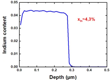
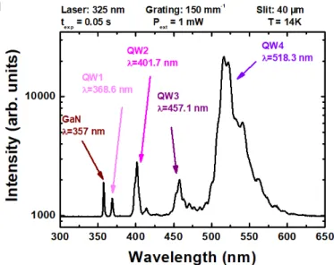
We grew two reference samples. Sample 1 (Fig. 1.22 (a)) consists in an InGaN buffer layer grown on a GaN template. The expected thickness is 300 nm. During the whole growth, the TMIn flux was maintained at a constant value. Based on previous experiments we expect an indium content of approximately 5%.
Sample 2 (Fig. 1.22 (b)) consists in four InGaN/GaN MQWs grown on a GaN template. The temperature was gradually decreased from QW to QW in order to have four different indium compositions. The expected indium contents are 5%, 10%, 15% and 20% respec-tively from the bottom to the top of the structure.
(a) (b)
Figure 1.22 – Structures of the reference sample 1 (a) reference sample 2 (b) (not to scale). nid stands for non intentionally doped.
Because of the nature of the InGaN alloy as described in 1.2.1, quantifying the indium content with accuracy is a complex problem. With all the following techniques, the In composition given below will be a mean composition of the analyzed volume.
1.4.1
Rutherford Back Scattering spectrometry (RBS)
The RBS technique is briefly described in annex C.7. It has been used previously to quantify In content in InGaN layers for instance by Pereira et al. [104].
Quantification in InGaN thick layer For our analyses, the chamber was main-tained under a vacuum of 2 × 10⁻⁶T orr. The ion flux was composed of 4He+ particles at
an energy of 2.3M eV . The analysis surface is of a few mm2. The retro-diffused particles
are analyzed with a detector at an angle of 160˚ from the initial direction. The detector yields the results as plotted in Fig. 1.23. On the absciss is plotted the energy of the par-ticles detected after retro-diffusion. On the ordinate is the number of parpar-ticles seen by the
![Figure 1.3 – Ga polarity and N polarity of wurtzite structure of GaN from [5].](https://thumb-eu.123doks.com/thumbv2/123doknet/12859335.368458/25.892.208.693.394.620/figure-ga-polarity-n-polarity-wurtzite-structure-gan.webp)
![Figure 1.14 – Direction of the Burgers vector of the wurtzite structure [74] (a) and the different types of dislocations [75] (b).](https://thumb-eu.123doks.com/thumbv2/123doknet/12859335.368458/40.892.163.722.138.384/figure-direction-burgers-vector-wurtzite-structure-different-dislocations.webp)

![Figure 2.6 – Emission spectrum of tri-chromatic white LED constructed by combining spectra from three separate orange (InGaAlP), green and blue LEDs (InGaN) (from [14].](https://thumb-eu.123doks.com/thumbv2/123doknet/12859335.368458/72.892.259.633.122.423/figure-emission-spectrum-chromatic-constructed-combining-separate-ingaalp.webp)