HAL Id: hal-01583770
https://hal.archives-ouvertes.fr/hal-01583770
Submitted on 3 Dec 2019
HAL is a multi-disciplinary open access
archive for the deposit and dissemination of
sci-entific research documents, whether they are
pub-lished or not. The documents may come from
teaching and research institutions in France or
abroad, or from public or private research centers.
L’archive ouverte pluridisciplinaire HAL, est
destinée au dépôt et à la diffusion de documents
scientifiques de niveau recherche, publiés ou non,
émanant des établissements d’enseignement et de
recherche français ou étrangers, des laboratoires
publics ou privés.
Manufacturing and testing of a metal supported
Ni-YSZ/YSZ/La2NiO4 IT-SOFC synthesized by
physical surface deposition processes
Jeremie Fondard, Pierre Bertrand, Alain Billard, Sébastien Fourcade, Pierre
Batocchi, Ghislaine Bertrand, Pascal Briois
To cite this version:
Jeremie Fondard, Pierre Bertrand, Alain Billard, Sébastien Fourcade, Pierre Batocchi, et al..
Manufac-turing and testing of a metal supported Ni-YSZ/YSZ/La2NiO4 IT-SOFC synthesized by physical
sur-face deposition processes. Solid State Ionics, Elsevier, 2017, 310, pp.10-23. �10.1016/j.ssi.2017.07.027�.
�hal-01583770�
OATAO is an open access repository that collects the work of Toulouse
researchers and makes it freely available over the web where possible
Any correspondence concerning this service should be sent
to the repository administrator:
tech-oatao@listes-diff.inp-toulouse.fr
This is an author’s version published in:
http://oatao.univ-toulouse.fr/24497
To cite this version:
Fondard, Jérémie and Bertrand, Pierre and Billard, Alain and Fourcade,
Sébastien and Batocchi, Pierre and Mauvy, Fabrice and Bertrand, Ghislaine
and Briois, Pascal Manufacturing and testing of a metal supported
Ni-YSZ/YSZ/La2NiO4 IT-SOFC synthesized by physical surface deposition
processes. (2017) Solid State Ionics, 310. 10-23. ISSN 0167-2738
Manufacturing and testing of a metal supported Ni-YSZ/YSZ/La
2
NiO
4
IT-SOFC synthesized by physical surface deposition processes
J. Fondard
a,b,c, P. Bertrand
c, A. Billard
a,b, S. Fourcade
d, P. Batocchi
d, F. Mauvy
d, G. Bertrand
e,
P. Briois
a,b,⁎aFEMTO-ST Institute (UMR CNRS 6174), Université de Bourgogne Franche-Comté, UTBM, 2 place Lucien Tharradin, F-25200 Montbéliard, France bFR FCLab 3539, 90000 Belfort, France
cICB (UMR CNRS 6303), Université de Bourgogne Franche-Comté, UTBM, 90400 Sevenans, France dICMCB-CNRS, 87 Av. du Dr. A. Schweitzer, 33608 Pessac Cedex, France
eCIRIMAT Université de Toulouse, CNRS, INPT, UPS, ENSIACET, 4 allée E. Monso, 31030 Toulouse, France
A R T I C L E I N F O
Keywords: SOFC
Metal support cell Thinfilms
Electrochemical measurement
A B S T R A C T
The manufacture of the last generation metal supported IT-SOFC complete cell by dry surface deposition pro-cesses is really challenging. Atmospheric Plasma Spraying (APS) and Reactive Magnetron Sputtering (RMS) processes are respectively adapted to deposit Ni-YSZ anode and YSZ electrolyte layers. RMS is also used to coat a thin and dense La2NiO4(LNO) cathode layer. In this work, we have realized a complete cell on metallic support
(ITM) produced by PLANSEE SE. The innovative LNO cathode layer was compared with screen-printed LNO layers, with and without RMS bonding layer. Electrochemical and Voltammetry tests were performed on these samples. It reveals lower performances than literature due to the high density of the RMS cathode layer, and too high temperature during sintering step which deteriorate layers manufactured by RMS and metallic substrate. Nevertheless, using LNO bonding layer manufactured by RMS seems to be an interesting way to improve the polarization resistance of the cell.
1. Introduction
Metal supported Intermediate Temperature Solid Oxide Fuel Cell is employed to face with the decrease of SOFCs operating temperatures. The switch from anode supported cells to this new technology allows significant gains in term of costs thanks to the mechanical support brought by the metallic piece[1]. Nevertheless, the use of a porous substrate presents some challenges. Thermomechanical and chemical compatibility problems between metallic and ceramic materials need to be solved. A diffusion barrier layer between metallic and ceramic ma terials permits to avoid the weakness of the substrate. A thin gadolinia doped ceria (GDC) layer applied, on the substrate, before the anode layer was identified as an appropriate solution to avoid Cr and Ni dif fusion [2]. Moreover, the oxidation of the support could cause the closing of its porosity, and deteriorate the performances of the cell[3]. Therefore, it is necessary to use elaboration techniques of ceramics with no requirement of heat treatment at too high temperatures. Dry de position techniques are a credible solution for the manufacturing of the core of the cell. Atmospheric Plasma Spraying process (APS) allows the realization of porous layers with very high deposition rate. This
technique is therefore perfectly adapted for the anode deposition on porous substrates[4]. Reactive Magnetron Sputtering (RMS) technique allows the deposition of thin and dense layers being able to be used as electrolyte[5]and diffusion barrier layers for the substrate/anode, and electrolyte/cathode [6]interfaces in fuel cells. Whereas thick layers realized by wet deposition techniques are commonly used as cathodes in IT SOFCs, recent studies deal with the deposition of Mixed Ionic and Electronic Conductors (MIECs) thin layers by physical surface deposi tion processes[7 8]. RMS process may also deposit a cathode layer by the co sputtering of several metallic targets[9]. La2NiO4is one of the
most promising materials in IT SOFCs thanks to its high stability in operation and its relatively low crystallization temperature. This K2NiF4
structured material also presents interesting electrocatalytic properties
[10], allowing its utilization as a thin cathode layer.
For this study, an ITM type porous metallic support manufactured by PLANSEE SE was employed for the cell assembling. This material presents very interesting thermal cycling resistance and durability properties keeping high electrochemical properties. A GDC barrier layer was applied on the top of the substrate by RMS. A common Ni YSZ anode material was deposited by APS on the metallic porous support
⁎Corresponding author at: FEMTO-ST Institute (UMR CNRS 6174), Université de Bourgogne Franche-Comté, UTBM, 2 place Lucien Tharradin, F-25200 Montbéliard, France.
E-mail address: pascal.briois@utbm.fr(P. Briois).
to produce two layers presenting different microstructures.
The powder used in these experiments was produced by spray drying process which consists in atomizing a suspension in a chamber where warm air circulates to dry atomized droplets. The spray drier used was a Mobile Minor from GEA Process Engineering. The suspen sion was formulated with 40.5 wt% of yttria doped zirconia (YSZ) particles with a d50of 0.3μm (Saint Gobain, France) and 59.5 wt% of
NiO powder with a d50of 0.4μm (Neyco, France). The tetragonal YSZ
powder was chosen thanks to its better mechanical properties than the cubic zirconia. A polyanionic dispersant PAA NH4 (polyacrylic acid,
P90 from Coatex, France) and a polyvinyl alcohol (PVA) as binder were used to complete the water based suspension formulation.
2.3. Screen printing (SP) process
Thefine La2NiO4 powder, produced by ourselves according to a
previous work[10], was mixed into a solvent with a commercial dis persant (terpineol) and binder (ethylcellulose). This ink was applied on samples by SP process (21 mm diameter, 3.14 cm2by using a semi
automatic screen printer Aurel MOD C890). A specific high tempera ture sintering treatment was required in order to obtain a good ad herence between the cathode layer of about 20μm in thickness and the electrolyte/or the bonding layer. The thermal cycle was as follows: an initial ramp at 1 K·min− 1up to 673 K to eliminate organic binders, followed by a temperature increase up to the sintering temperature at 3 K·min− 1. In order to avoid the deterioration of the metallic substrate, sintering step was performed at 1423 K under nitrogen.
2.4. Characterization devices
The morphology of the coatings/powders was characterized by Scanning Electron Microscopy (SEM) using a JEOL JSM 7800 F equipped with Energy Dispersive Spectroscopy (EDS) for chemical measurements. The structural features of the supports and coatings were performed in Bragg Brentano configuration X ray diffraction using a BRUKER D8 focus diffractometer (Co Kα1 + α2radiations) equipped
with the LynxEye linear detector. XRD patterns were collected at room temperature during 10 min in the [20° 80°] scattering angle range by steps of 0.019°. Samples roughness was measured by an Altisurf pro filometer by the means of an optical sensor without contact. This measure is conducted along a distance of 17.5 mm with 10 measures
per line. A surface of 100 mm2 was explored and roughness char
acteristics were calculated after signalfiltration and wave component removal. The surface of the samples was hand polished with SiC papers with alcohol as lubricant. 600, 800, 1200 and 400 SiC papers were used to smooth the surface and to remove 60μm of the coating thickness.
Then, the final polishing was done with 1 μm diamond paste and
0.25μm OPS solution. The powder size distribution is was determined by a Mastersizer 2000 laser granulometer. The optical transmittance measurements were performed with a UV visible NIR Shimadzu UV 3600 Spectrophotometer control by UV probe 2.33 software. All mea surements were carried out between 380 and 780 nm on glass slides. 2.5. Single cell tests
The SOFC samples were inserted into a homemade set up designed and built in the ICMCB laboratory. A nickel/gold grid was maintained on the cathode side with springs for current collection. Cathode layer was sintered for better crystallization at 1073 K during 10 h under air and in the same time, the anodic part was set under neutral gas con ditions to avoid substrate deterioration. After, the anode layer was re duced in situ step by step with H2/Ar mixtures at 973 K during 6 h.
Electrochemical measurements were performed at 973 K with
120 mL·min− 1 flow of H2 3 vol% H2O on the anode side and
240 mL·min− 1 air flow on the cathode side. The parameters for the Voltammetry measurements were 2 s equilibrium time, starting from
[11]. Then, YSZ electrolyte and GDC barrier layers were applied by
RMS after the polishing of the anode surface. Most RMS coatings were deposited with the help of a Plasma Emission Monitoring (PEM) system, increasing the deposition rate of ceramics [12]. LNO cathode layer was
successively deposited by RMS by co sputtering of two metallic targets with PEM system [13]. In order to compare the efficiency of the ex
perimental layer deposited by RMS as an individual cathode (RMS LNO) or a bonding cathode layer, the complete IT SOFC building was realized by replacing and/or adding a screen printed La2NiO4 material (SP
LNO). This layer was developed, and optimized in ICMCB laboratory and allows interesting performances on LNO/GDC/LNO half cells [14].
The overall cell performance comparison and detailed impedance analyses of the three different cells containing RMS LNO, SP LNO, and RMS LNO + SP LNO are presented to elucidate the difference between the complete cells.
2. Experiments
2.1. Reactive Magnetron Sputtering (RMS) process
Two experimental devices were used for the different deposition processes. Systems are pumped down via a system combining XDS35i Dry Pump and a 5401CP turbo molecular pump. Metallic targets were powered by a pinnacle + pulsed current generator from Advanced Energy. The ceramic coatings were synthesized in an argon and oxygen atmosphere. The flow rates were controlled with Brooks flowmeters and the pressure was measured using a MKS Baratron gauge.
A thin GDC layer was first applied on ITM metallic supports pro vided by PLANSEE SE. The experimental Alcatel604 device was used for this coating. The sputtering chamber was equipped with four 50 mm diameter magnetron targets with a 250 mm rotating substrate holder parallel to the target at 120 mm. Samples were positioned at 55 mm from the axis of the substrate holder. Coatings were made by the co sputtering of two Ce and Gd metallic targets with 120 sccm (standard cube centimeter per minute) argon and 5 sccm oxygen flow rates.
All the RMS coatings deposited after the APS coating were per formed in a 100 litre Alcatel SCM 650 sputtering chamber pumped down. The sputtering chamber was equipped with three 200 mm dia meter magnetron targets and with a 620 mm diameter rotating sub strate holder parallel to the targets at a distance of about 110 mm. Zr Y (84 16 at.%), Ce Gd (80 20 at.%), La and Ni metallic targets were used. Substrates were positioned in front of the target at 170 mm from the axis of the rotating substrate holder in order to deposit homogenous coatings in terms of thickness and composition. The deposition stage was monitored using a closed loop control PEM (Plasma Emission Monitoring) system by optical emission spectroscopy (OES). The tech nique was based on the measurement of the optical intensity of the metal emission line in a volume near the target [12]. The signal was
sent via an optical fiber to a Ropper Scientific SpectraPro 500i spec trometer, with a 1200 groove mm− 2 grating and a photomultiplier tube
(Hamamatsu R 636). Subsequently, the information was transferred to a computer in which a program developed under Labview® controls the oxygen flow rate for keeping the optical intensity IZr∗ constant.
2.2. Atmospheric Plasma Spraying (APS) process
The plasma is generated in air at atmospheric pressure (APS) by a F4 plasma torch with a 6 mm internal nozzle diameter. A mixture of argon and hydrogen is used to form the plasma. The powder is injected by the means of argon carrier gas. It is introduced into the plasma via a 1.8 mm injector positioned at 6 mm from the exit of the torch with a 90° angle. 1 mm thick ITM samples provided by Plansee S.E. (Reutte, Austria) with 25 mm diameter were positioned on a fixed holder at a distance of 90 mm from the plasma torch. The torch was controlled by a robot programmed to sweep sample surface with a step of 5 mm at a speed of 150 mm·s− 1. Different operating conditions were used in order
OCV potential, to 0.2 V end potential with 5 mV·s− 1 scan speed. Electrochemical Impedance Spectroscopy (EIS) measurements were then collected at the Open Circuit Voltage (OCV) in the frequency range 100 MHz to 10 MHz with 10 points per decade.
3. Elaboration and characterization
3.1. Elaboration of the GDC barrier layer by Reactive Magnetron Sputtering (RMS)
This protective layer was coated on the top of the ITM metallic porous substrate by the co sputtering of two Ce, Gd metallic targets in the stable sputtering conditions. The appropriate conditions to obtain an adherent Ce0.8Gd0.2O2(GDC20) coating on highly porous substrates
were optimized. Studied and optimized deposition parameters are presented inTable 1. The oxygen and argonflow rates were fixed at 5 and 120 sccm respectively. Arflow rate was chosen in order to avoid delamination of thefilm under high compressive stress caused by the high weight of the Gd and Ce atoms [15]. First of all, the intensity applied on the Ce target was determined byfixing the parameters on Gd target at 0.3 A. This value was chosen to reach a sufficient deposition rate without fast consumption of the target. Intensities of 0.85 and 1 A on Ce target produced 18 and 11 Gd at.% respectively, giving the GDC structure. A higher discharge frequency was used to initiate the sput tering of the Gd target at this high pressure. Coatings were also produce for increasing time period to monitor the Gd content in the cerium oxide structure. In stable conditions with high pressure, the deposition
rate appears to be low to obtain a 1.5μm thick coating
(≈300 nm·h− 1). After 3 h of deposition stage, the voltage of the target
was increased by 60 V, lowering the average Gd content in the coating. This is due to the relatively low dimension of the target compared to its fast sputtering efficiency degradation. To solve this problem, coatings were deposited in two 2 h 30 deposition steps. Optimized deposits present 14 at.% Gd content with the appropriate GDC20 structure.
Fig. 1presents the morphological features of this coating on ITM substrate. Surface observations reveal a covering deposit in spite of the high porosity and roughness of the substrate (Fig. 1.a, b). This is con firmed by cross section images (Fig. 1.c). This coating presents cracks due to the morphology of the substrate and the strain relaxation during oxygen incorporation inside the structure (Fig. 1.d).
3.2. Elaboration of the anode bi layer by Atmospheric Plasma Spraying (APS)
A 59.5 wt% NiO and 40.5 wt% YSZ powder is used as the feedstock material.Fig. 2presents the characteristics of this powder. Unexpected large particles of NiO are clearly identified whereas the zirconia par ticles are in the same size range as the raw material. Therefore the distribution of both materials is not homogenous in the agglomerated powders (Fig. 2.a). The spray dried powder was sieved in order to ob tain two different powder size ranges inferior and superior to 50 μm respectively. These two different size distributions of the spray dried
powders were used for the synthesis of each anode layer (Fig. 2.b). The larger size powder was used for the deposition of the lower layer near the porous metallic support in order to obtain large porosities. The smaller one was used for the upper layer near the electrolyte in order to obtain small porosities and low roughness. The anode layer must pro vide good mechanical strength andfill the large pores in the substrate (40 vol% porosity) that are between 20 and 60μm.
Thermal spraying deposition conditions are shown inTable 2. These conditions were chosen thanks to a previous study[16]. The Ar/H2
ratio highly influences the composition and the porosity due to different plasma temperatures and speeds. Higher Ar/H2 ratio increases the
coating porosity and decreases Ni losses due to lower plasma tem perature. The powder size is also important to produce small and large porosities. Smaller grains are melted easily and the splats produced during the deposition are smaller too.
Fig. 3presents the roughness of the substrate (Fig. 3.a.), the anode as deposited (Fig. 3.b.) and the anode after polishing (Fig. 3.c). This figure shows that the realization of the APS anode layer reduces the roughness of the substrate influence. However, the surface remains too rough. A polishing treatment is necessary to smooth the surface and to favor the deposition of a thin and dense YSZ layer by RMS process. This polishing treatment is very efficient to reduce the roughness and finally, the surface quality is significantly improved.
The composition analyses determined by EDS (shown inTable 3) on reduced samples (in an Ar/H2(80/20) mixture at 873 K for 3 h) prove
the influence of the thermal spraying parameters. The Ni ratio is higher in the lower layer. Nevertheless, the Ni content might be too low to ensure percolation in the upper layer (30 vol% Ni is needed). This loss of nickel is imputed to the higher proportion of hydrogen in the plasma used to produce the upper layer, which leads to a reduction of NiO to Ni and causes its volatilization. This phenomenon is confirmed by the XRD analysis of the structure of the coatings where NiO and Ni phases were clearly identified (Fig. 4).
Fig. 4presents the structure of the coating as deposited and after reduction. The presence of tetragonal YSZ, NiO, Ni and an additional
phase are identified. The additional phase could be described as
shoulders or splitting of all the YSZ peaks. Therefore as no JCPDS da tasheets could be attributed to this pattern, we hypothesized that it is related to a YSZ phase with a different lattice parameter. This change could be ascribed to an incorporation of Ni in its structure.
SEM observations on the BSE mode of the coating after reduction, and cartographies of the different layers are presented inFig. 5. The different layers are visible in this micrograph. Cartography shows the repartition of the different elements. There is Ni stripes in an YSZ matrix. The porosity of the samples presented inTable 3are calculated by averaging over 20 pictures by image analysis from the ImageJ software. The porosity difference between the two layers, which is around 15 vol% for the upper layer and 30 vol% for the lower one, is easily noticeable in thisfigure. Bi layer morphology permits to cover the substrate porosity and to optimize the electrochemical properties. 3.3. Deposition of the YSZ/GDC electrolyte layer by Reactive Magnetron Sputtering (RMS)
This coating is deposited from a metallic Zr/Y target (84/16 at.%) and Ce/Gd (80/20 at.%) controlled by the Plasma Emission Monitoring system.Table 4summarizes the preparation conditions of the electro lyte. The objective is to obtain a dense and high temperature resistant coating in view of the cathode elaboration. The parameters were opti mized in a previous work[16]. Samples are deposited on APS anode layers and on commercial NiO YSZ anodes screen printed type III pro duced by Jülich in order to assess the influence of the APS anode layer.
Fig. 6presents the hysteresis loops obtained with the different targets.
Sputtering a metal target in argon oxygen gas mixtures generally leads to a sputtering instability regime phenomenon with a low deposition
rate to obtain ceramic films. To avoid the drawbacks of this
Parameters Studied Optimized Deposition distance (mm) 60
Argonflow rate (sccm) 120 Oxygenflow rate (sccm) 5
Deposition time (h) 2–6 2∗ 2 h30 = 5 Parameters applied on Ce target
Intensity (A):frequency (Hz):Toff(μs)
0.85–1:50:5 0.85:50:5 Parameters applied on Gd target
Intensity (A):frequency (Hz):Toff(μs)
0.3:70:5 0.3:70:5 Deposition rate (nm/h) 300
Table 1
phenomenon, control of oxygen levels in the reactor via closed loop is used in order to achieve the optimal deposition rate.
For both metallic targets, increasing and decreasing the oxygenflow rate produces a hysteresis loop corresponding to unstable sputtering conditions. An oxygen doped metal layer is deposited for lower oxygen flow rates with high deposition rate. The optical signal remains in the same order of magnitude than without oxygen. When the entire target is oxidized around 6 and 7 sccm of O2for Zr Y and Ce Gd respectively,
the optical signal drops. Then, an oxide is deposited with low deposi tion rate. When the oxygenflow rate decreases, the optical signal raises at an oxygenflow rate between 2 and 3 sccm. Using PEM allows the deposition of oxide layers under unstable conditions (inside the hys teresis loop), in this case the ceramic was synthesized with higher sputtering rate. The emission line of zirconium (360.12 nm) and cerium
Fig. 1. SEM observations of the GDC layer deposited on the ITM porous metallic substrate. Morphology of the surface (a, b). Cross sections of the coating (c, d).
Fig. 2. NiO-YSZ powder characteristics. Table 2
Thermal spray deposition conditions.
Parameters Upper layer Lower layer Feedstock NiO-YSZ powder (59.5–40.5 wt%) Standoff distance (mm) 90
Carrier gasflow rate (L/min) 3.5 3.5 Voltage (V) 64.8 58.5 Current (A) 500 500 Primary gaz (Ar) (L/min) 35 50 Auxilary gaz (H2) (L/min) 8 3
(418.66 nm) were used to plot the evolution of the optical emission as a function of the oxygenflow rate inFig. 6a and b respectively. It can be noticed that setpoints can easily be maintained inside the loop (open points).
Fig. 7shows the surface morphology of the samples after the dif ferent deposition steps (anode as deposited on porous support (a) and after polishing (b), YSZ after annealing on polished anode (c) and on commercial NiO YSZ anode support (e), GDC after annealing on porous support (d) and on commercial anode support (f)). The surface mor phology of the YSZ layer deposited on a polished APS anode on porous
support presents a rather smooth shape with some holes whereas there are only a very few defects on the coating deposited on a commercial anode support. Defects seem to come from the support through the anode layer, even after polishing (Fig. 7.a,b) and should be further improved. The addition of a GDC layer increases the recovering of the electrolyte on the anode side (Fig. 7d).
Fig. 8presents the XRD patterns of the YSZ and GDC layers after a baseline with alumina powder. Peaks move towards higher Bragg an gles, which is consistent with a decrease of the lattice parameters. This may be due to oxygen incorporation in the structure during the an nealing which provokes contraction of the lattice. According to litera ture, this technique is efficient to deposit dense coatings on porous substrates[17 18].
3.4. Deposition of the La2NiO4cathode layer by reactive magnetron
sputtering
This coating was deposited by co sputtering of La and Ni metallic targets. The deposition conditions were studied in detail in a previous study[13].Table 5summarizes the optimized conditions to deposit this layer.
Fig. 3. Surface condition and roughness of samples by profilometry measurements.
Table 3
Composition of different layers after reduction.
Powder Upper layer Lower layer Ni (at.%) 28.74 ± 0.99 36.69 ± 1.92 Zr (at.%) 22.63 ± 0.65 20.72 ± 1.95 Y (at.%) 1.36 ± 0.10 1.22 ± 0.21 O (at.%) 47.27 ± 1.24 44.16 ± 1.77 vol% Ni 39.1 24.77 ± 0.01 31.55 ± 0.02 % porosity 15 30
Because ITM substrate is a metallic support which is sensitive to oxidation, crystallization has to be performed in low oxygen partial pressure. Tests have been performed to crystallize the LNO coating deposited on a YSZ substrate under nitrogen gas at 1173 K. Fig. 9
presents XRD patterns after this annealing treatment compared with coatings crystallized under air conditions. These lower oxygen partial pressure conditions allow the crystallization of orthorhombic lan thanum nickelate phase contrary to the air conditions annealing where the tetragonal structure was identified. Moreover, these special condi tions destabilize the most important phase and produce a mixture of lanthanum oxide and nickel metallic phases as shown inFig. 9. This typical behavior was also demonstrated in the literature [19]. In this work, the reduction of the oxygen partial pressure lowers the destabi lization temperature of the La2NiO4structure into La2O3and Ni mix
ture. Then, at 1373 K, this mixture appears systematically under
Fig. 4. XRD pattern of powder anode layer as-deposited and after reduction.
Fig. 5. SEM micrographs of the different anode layers on polished cross section. Table 4
Reactive Magnetron sputtering deposition conditions using Plasma Emission monitoring system (PEM). Target Draw distance (mm) Parameters applied on target Arflow rate (sccm) Setpoint (%) Deposition rate (μm/h) Zr/Y (84/ 16 a-t.%) 110 2.5 A, pulsed with 50 kHz, 5μs 25 40 1.13 Ce/Gd (80/ 20 a-t.%) 50 0.78
Fig. 6. Hysteresis loop of the different targets used with PEM system: YSZ (a), GDC (b).
pO2= 10− 10Pa[19]. Therefore, for the complete cell building, the
crystallization is chosen to be performed during the single cell tests where the cathode side is under oxygen atmosphere and support under reductive atmosphere. Under these conditions, the cathode mainly crystallized under nickelate structure with small La2O3impurity phase
and it avoids the substrate deterioration (i.e. oxidization of metal support). This step has been performed at 1073 K during 10 h.
3.5. Complete cell building
Fig. 10shows the brittle fracture cross section of the complete cell built on ITM porous supports (a, b). The as deposited La Ni O layer can
be seen in the fracture cross section (Fig. 10.b). It exhibits a columnar structure, and it is well adherent to the GDC layer. In a previous study, it was demonstrated that the microstructure of the layer changed after crystallization: the layer loses its columnar shape and becomes denser
[13]. All layers are adherent and perfectly covering.
In the following part, the cell performance and electrochemical analyses of this cell (named RMS LNO) will be detailed. Two other samples were synthesized. On the one hand, the last La2NiO4 layer
manufactured by Reactive Magnetron Sputtering (RMS LNO) was re placed by a La2NiO4layer manufactured by Screen printing (SP LNO) to
compare both cathodes. On the other hand, a screen printed La2NiO4
layer is added on the top of the deposited cell to form a single cell presenting both RMS and SP cathode layer. In this architecture, the RMS layer is a bonding layer for the porous layer (RMS + SP LNO). The
Table 6summarized the thickness of each component of the different configuration.
4. Single cell tests
As previously described, anode reduction and cathode crystal lization (only RMS LNO sample) were performed in the single cell bench. Each step was described in the experimental part. Increasing air
Fig. 8. XRD differences between as-deposited and annealed coatings of YSZ and GDC.
Table 5
Reactive Magnetron sputtering deposition conditions using Plasma Emission monitoring system (PEM). Target Draw distance (mm) Parameters applied on target Arflow rate (sccm) Setpoint (%) Deposition rate (μm/h) La 110 2.5 A/50 kHz 50 60 1.35 Ni 0.54 A/50 kHz
Fig. 9. XRD patterns of the LNO coating crystallized under air and under low oxygen partial pressure (nitrogen gas).
flow rate leads to improve the OCV of the cells. The Open Circuit Voltage (OCV) of the cells with RMS LNO and SP LNO was measured at 0.9 V after cathode crystallization and anode reduction processes. This value is lower than the theoretical value of 1.02 V at this temperature and proves that the electrolyte tightness is not fully achieved. With SP LNO coated on RMS bonding layer, OCV increases up to 0.95 V, pointing the efficiency of this additional layer. Differences between RMS samples and others are due to the previous cathode crystallization process of RMS cathode layer. This additional step (1073 K during 10 h) initiates the reduction process when the anodic side of the cell contains little hydrogen gas (95:5 vol% N2:H2). This results to higher initial OCV
(0.21, 0.01 and 0.02 V for RMS, SP and RMS + SP samples respec tively). The difference between samples with and without RMS bonding layer at each reduction step underlines its efficiency in this system. Indeed, OCV of sample presenting the bonding layer increases faster and the final value is higher (0.90 and 0.95 V for SP and RMS + SP respectively). Tests have also been performed on cells manufactured on commercial anode supported cells, containing RMS LNO layer. The OCV value remains the same as the cell built from a metal substrate (i.e. 0.90 V). The low number of defects identified in the YSZ layer (Fig. 7.b) does not influence the tightness of this layer. Therefore, no negative
effect of the metallic substrate or the thick anode layer is identified on the voltage characteristics.
After 3 h of stabilization, single cell tests are performed.Fig. 11
presents voltammetry tests of these cells. These measurements indicate a maximum power density of 60, 71 and 76 mW·cm− 2. In the literature, metal supported cells with anode and electrolyte manufactured by plasma spraying process and LSCF by screen printing reach a power density of 500 mW·cm− 2at 1073 K[20]. Cells presenting an electrolyte layer manufactured by reactive magnetron sputtering, reach a power density of 410 mW·cm− 2at 973 K[21]and the presence of a really thin YSZ electrolyte with LSCF made by screen printing can allow to reach
much higher power densities [22]. Some improvements of the cell
microstructure and reduction of the thickness have to be performed in order to obtain better performances.
The electrochemical performances obtained with these different samples are in the same order of magnitude but SP LNO cathodes present higher power densities maybe due to higher active surface area. The RMS bonding layer allows an improvement too. This may increase the contact surface between the electrode and the electrolyte.
According to the Ohm law, the total resistance of the cell can be determined by the slope calculation from the experimental I E curve. In the low current density range, the ohmic resistance of the cell pre senting RMS cathode is close to 3.4Ω·cm2and the resistance of the other cells is 3.1Ω·cm2. Nevertheless, as shown in theFig. 11, at higher
current density, the ohmic resistance of the SP LNO sample falls at 2.5Ω·cm2. This improvement might be induced by a switch between activation polarization and ohmic polarization. This observation con firms that the low performances observed could be due to electrode overpotentials.
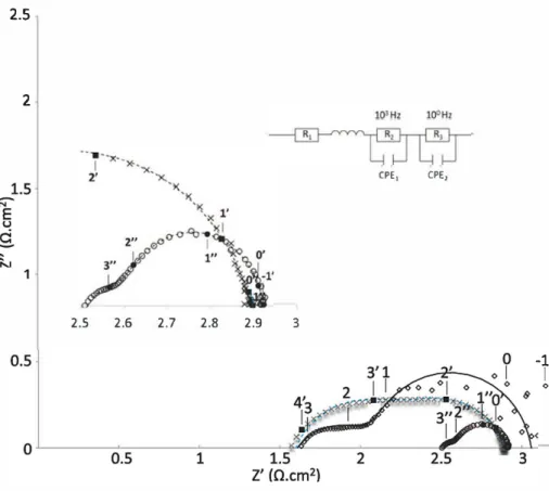
To explain these low performances, Electrochemical Impedance Spectroscopy (EIS) characterizations were also performed on these samples.Fig. 12presents typical Nyquist measurements of the complete cell under OCV. The Nyquist diagrams werefitted using Z View soft ware. Modeled data are represented by lines in thefigures while ex perimental measurements are represented by data points. Four con tributions characteristic of different phenomena appearing were identified in high, medium and low frequency ranges. Resistance and associated capacitance values were extracted from thesefits. Besides Nyquist diagrams werefitted by the same equivalent circuits, shapes of the impedance diagrams are fundamentally different, depending only on the cathode layer characteristics. Total resistances in the low fre quency range are in the same order of magnitude, explaining perfor mances measured on the different samples (Fig. 11). These different characteristics attributed for medium or low frequencies underline the different electrochemical phenomena occurring in the different sam ples. The resistance at high frequencies remains the same with“RMS”
and “SP” samples but it is considerably higher with “RMS + SP”
sample. The dense bonding cathode layer seems difficult to cross and induces two more interfaces. Nevertheless, this layer allows an
Fig. 10. Cross section observation of a complete cell deposited on ITM porous support (a) and electrolyte/cathode (b). Table 6
Thickness of each part of complete cell in micrometer.
Configuration RMS SP RMS + SP Component
Anode (NiO-GDC) 150 Electrolyte (YSZ) 10 Buffer layer (GDC) 1.3
Cathode (La2NiO4) 2 30 32
Fig. 11. Voltammetry tests of complete cells with RMS cathode, SP cathode and RMS + SP cathode layers.
2.5
2
CPE1
2.5 2.6 2.7 2.8 2.9 3
interesting drop of the polarization resistance of the complete cell. In spite of its several interfaces and resistances, complete cell resistance remains the lowest. A decrease of the bonding layer thickness should considerably improve performances.
On the basis of the fitted data, the equivalent capacitance and the frequency relaxation of each contribution were calculated using rela tions Eqs. (1) and (2).
Ceq = ReCl-nl/; c1/.
(1) With R: electrical resistance, n: decentering angle of the Constant Phase Element function, C: capacitance of the phenomenon.
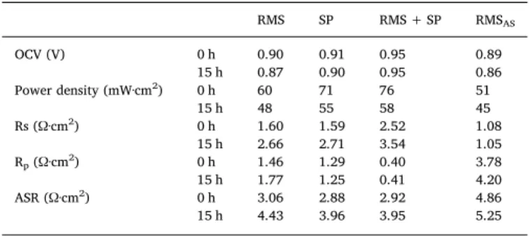
(2) Table 7 presents the parameters of the different phenomena for each sample including a cell synthesized on a commercial anode support with RMS cathode. High, Medium and I..ow frequency phenomenon are named by 1 (Ri, Ceqi, f1), 2 CR2, �. f2l and 3 (R3, �. f3) respec tively. Polarization Resistance CR.,) is calculated by the sum of R2 and R3. ASR represents the complete cell resistance.
Complete cell resistances ASR are much higher than requirements for IT SOFCs (i.e. 0.8 Q-cm2). These high values explain the poor Table 7
Parameters detennlned by l!lectrodtemlcal lmpedanœ Spectroseopy at 973 K.
RMS SP RMS + SP RMSAs HF R1 (Q-cm2) 1.60 1.59 2.52 1.08 MF R, (Q-cm2) 0.52 0.70 0.07 0.79 Ceq,(F·cm ') 2.8 10 3 3.7 10 4 9.410 3 6.910 4 f2 (Hz) 2.4 lo' 5.0 104 7.7 103 3.2 104 LF Ra (Q-cm2) 0.94 0.59 0.33 2.99 Ceq.(F·cm ') 2.910 1 8.8 10 2 1.210 1 3.010 1 f3 (Hz) 2.5 10° 3.8 1<>2 2.4 101 8.810 1 R,, (Q-cm2) 1.46 1.29 0.40 3.78 ASR (Q-cm2) 3.06 2.88 2.92 4.86 CPE,
-1
1
◊Fig. 12. Nyquist plots of complete cens with RMS cathode, SP cathode and RMS + SP cathode layers. Models are re presented by Hnes. Experimental results are represented by points. Symbols represent the dlfferent samples: SP LNO (X). RMS LNO (◊). RMS + SP LNO (O).
performances obtained with these samples at 973 K. Numerous limita tions should be induced by the use of several layers synthesized by different deposition techniques. The compatibility of these materials and structures has to be optimized in order to improve the perfor mances by decreasing resistances.
According to the relaxation frequency and the equivalent capaci tance values, three domains can be distinguished, at high frequency (HF), middle frequency (MF) and low frequency (LF), each representing a given electrochemical phenomenon. These results are presented in
Table 7.
Using the Schouler's method [23), resistance and CPE have been assigned to specific electrochemical proœsses. According to literature on cathode half cells with YSZ and GDC electrolyte, the low frequency range (LF) is characterized by high capacitance values, Ceq "" 1 10 F-cm -2 [14,24). This contribution was assigned to the
gaseous diffusion through the electrode. The capacitance of the medium frequency contribution (MF) is found to be higher, Ceq "" 10-3 10-1 F-cm -2• The source of this impedance contribution
is more complicated to identify, it has been assigned to Oxygen Re duction Reaction (ORR) itself occurring at the electrode/gas interface
[14,25) and/or ionic transfers at the electrode/electrolyte interface
[26).
Because cathode material is the only variable parameter and be cause resistances and capacities are different, polarization resistance should be due to cathode material. Furthermore, single cell tests were performed on samples built on a commercial anode support with RMS cathode. LF phenomenon seems to be identical on the two samples (2.9 X 10⁻¹ F-cm-2 and 3.0 X 10⁻¹ F-cm-2 for RMS and RMSAS re
spectively) confirming that this phenomenon could be due to the cathode. Nevertheless, equivalent capacitance and relaxation fre quencies remain slightly different at MF. This difference could be re lated to cathode and/or anode electrochemical phenomenon. Calculated values are close to 10-3 F-cm -2 for the MF range and
1 F-cm -2 for the LF range (Table 7). Furthermore, resistance values of
the MF are significantly improved by the addition of the bonding layer (0.70 O-cm2 and 0.07 Q-cm2 for SP and RMS + SP respectively).
Bonding layer acts as an interface layer with the cathode material, this MF phenomenon could be assigned to ionic transfer at the electrode/ electrolyte interface. From these two last contributions at MF and HF, electrode polarization resistances of 0.4, 1.3, 1.5Ω·cm− 2 were de
termined for RMS + SP, SP and RMS respectively. Nevertheless, the specifications of fuel cell electrodes are lower than 0.5 Ω·cm− 2 The
resistances obtained on RMS and SP samples are too high but probably not because of the same reasons.
Each sample has been measured again after one night ageing (i.e. 15 h) in order to see the cell stability. Results of each cell are presented inTable 8. In all cases, OCV remains stable but performances fall during this time, indicating the instability of the single cell components. This drop is even worse with samples fabricated on metallic substrates with APS anode layer (12, 20, 22 and 24% decrease for anode supported cell with RMS LNO, metal supported cells with RMS LNO, SP LNO and RMS + SP LNO respectively). Therefore, metal substrate and/or APS anode layer are not stable in these conditions. EIS measurements allow to identify the limiting factor in all cases. Only the polarization resistance increases in the anode supported cell. The resistance of MF phenom enon is constant when LF increases (3.5 and 4.2Ω·cm2before and after
ageing respectively). The degradation is due to electrochemical char acteristics of commercial anode and/or cathode. Opposite behavior is demonstrated with metal supported cells presenting SP LNO cathodes where the serial resistance increases contrary to polarization resistance. Serial resistance can be due to poor electrical contacts between the
different components. Finally, with RMS LNO sample made on metal
substrate, the degradation occurs on each layer because both re sistances increase during this period.
Analyses of structures and microstructures of electrolyte, cathode and interface have to be checked to point out differences between samples and explain results.
5. Characterizations after tests
Fig. 13presents the structure comparison of the cathode materials after the electrochemical tests were performed. Due to a thin cathode layer on the RMS sample, GDC structure is identified. According to a previous work[13], the RMS sample presents a small diffraction peak of La2O3phase. This behavior is attributed to a metallic ratio La/Ni
slightly higher than 2. XRD patterns of SP and RMS + SP samples re main the same because the cathode layer is too thick to identify the bonding layer. An unidentified peak related to the satellite (113) dif fraction line, appearing at lower angle, is ascribed to the Co Kβcon
tribution of X ray beam, and can be detected only when the material is well crystallized. This is the reason why that peak appears on the SP cathode and not on the RMS cathode that presents a thinner micro structure. The same tetragonal lanthanum nickelate phase as the one identified inFig. 9was identified without major impurities. A slight preferential orientation difference could be noted between cathode deposited by RMS and SP. It should have no effect on cathode char acteristics.
Fig. 14shows SEM observations of surface microstructure of the different samples after the tests. The surface of the samples with RMS and SP cathode layers are rather smooth but it can be noticed on the surface of the RMS deposit some defects (Fig. 14.a,c). These defects should not involve electrochemical problems. At higher magnification, the microstructure of the cathode coatings is totally different, as ex pected. While RMS coating is fully dense, SP coating present high content of porosities. SEM observations of samples cross sections are presented inFig. 15. Samples presenting LNO cathode manufactured by screen printing process need high temperature sintering treatment to optimize the adherence of the layer. This annealing treatment (1423 K for 12 h under nitrogen atmosphere) induces microstructural changes. While sample with RMS LNO layer presents dense layers (Fig. 15.a), sintered samples present more porosities (Fig. 15.b, c). Indeed, small sized porosities appear in all RMS layers and at interfaces. Image ana lyses have been performed by Image J software on SEM micrographs. It reveals 10 ± 2% porosity with 0.006 ± 0.004μm2surface (≈90 nm
average porosity diameter if considered as perfect sphere) inside the electrolyte layer on RMS + SP sample, and 16 ± 3% porosity with
0.024 ± 0.009μm2 surface (≈180 nm average porosity diameter).
Nevertheless, this analysis was not done on RMS sample. This increase of the porosity is a well known phenomenon occurring in coatings de posited by EB PVD. Space between thin and thick columns increase during high temperature annealing and spherical porosity appears along the thicker column[27]. However, the porosity appearing in the electrolyte (Fig. 15b,c) is not connected and open because the OCV of the cell remains the same for RMS and SP samples (i.e. 0.9 V). RMS LNO
RMS SP RMS + SP RMSAS OCV (V) 0 h 15 h 0.90 0.91 0.95 0.89 0.87 0.90 0.95 0.86 Power density (mW·cm2) 0 h 15 h 60 71 76 51 48 55 58 45 Rs (Ω·cm2) 0 h 15 h 1.60 1.59 2.52 1.08 2.66 2.71 3.54 1.05 Rp(Ω·cm2) 0 h 15 h 1.46 1.29 0.40 3.78 1.77 1.25 0.41 4.20 ASR (Ω·cm2) 0 h 15 h 3.06 2.88 2.92 4.86 4.43 3.96 3.95 5.25
Fig. 13. XRD patterns of RMS, SP and RMS + SP complete cells. Table 8
Fig. 14. Surface microstructure of samples with RMS (a,c) and SP cathodes (b,d) at different magnifications.
layer does not present columnar structure as shown inFig. 10b. This morphology evolution was induced by the high annealing treatment during the SP LNO process. This fact could involve different electro chemical performances between RMS cathode and RMS bonding layer. EDS profiles and mappings, performed on polished cross section of samples, confirm a slightly lack of lanthanum but not significant. No
element diffusion was detected between electrolyte and cathodes,
showing the chemical stability of these layers (Fig. 16). The increase of porosity, induced by the sintering treatment of the SP LNO cathode, may improve electrochemical behavior of the bonding layer but it provokes porosity inside the electrolyte and interfaces with GDC layers which slow the ionic diffusion. These phenomena could increase re sistances and explain the poor performances of the cells.
Fig. 16shows the EDS mapping of the porous metallic support for the different samples after the electrochemical tests. All the samples present a thin Cr2O3 oxidation protective layer but it seems to be
thicker with SP sample, due to higher annealing time and temperature, even at very low oxygen partial pressure conditions (nitrogen gas). Results found in literature confirm the formation of a chromium oxide layer on metallic support in these conditions, but no evidence of da mage was pointed in these works[3,22]. Nevertheless, chromium oxide layer should act as electronic diffusion barrier and could impact per formances. No nickel and/or chromium interdiffusion between support and anode layer was evidenced proving the positive effect of the GDC protective diffusion layer also reported in some studies[2]. Moreover, no nickel agglomeration was observed in the anode layer in the present
study, in contrast to the results mentioned in some publications for long
term annealing treatment [28]. These compositional and micro
structural modifications of the substrate could explain the poor per formances of the cells.
6. Conclusion
A GDC/Ni YSZ/YSZ/GDC/La2NiO4complete cell was deposited on
porous metallic substrates, provided by Plansee SE, by dry deposition processes and successfully tested at 973 K in air and hydrogen atmo sphere. The bi layer anode with different architectures, porosities and compositions was deposited on the substrate by plasma spraying in atmospheric conditions. This technique allowed covering the surface porosity, limiting the roughness and increasing the number of contacts with the electrolyte layer. Nevertheless, a polishing treatment is ne cessary in order to smoothen the surface of the samples. The YSZ electrolyte and GDC protective layers were deposited by reactive magnetron sputtering using the PEM process to deposit sub stoichio metric coatings expected to further be densified after their full oxidizing heat treatment. In order to preserve the cell, YSZ coating was performed by two deposition stages, each of them followed by an annealing treatment. La Ni O stoichiometric coating with La/Ni atomic ratio equal to 2 was deposited from co sputtering of La and Ni targets. The anode reduction and cathode crystallization processes were performed in the single cell bench to avoid degradations.
This RMS LNO cell was tested and results compared with data
[1] M.C. Tucker, Progress in metal-supported solid oxide fuel cells: a review, J. Power Sources 195 (2010) 4570–4582.
[2] P. Blennow, J. Hjelm, T. Klemenso, S. Ramousse, A. Kromp, A. Leonide, A. Weber, Manufacturing and characterization of metal-supported solid oxide fuel cells, J. Power Sources 196 (2011) 7117–7125.
[3] M. Brandner, M. Bram, J. Froitzheim, H.P. Buchkremer, D. Stöver, Electrically conductive diffusion barrier layers for metal-supported SOFC, Solid State Ionics 179 (2008) 1501–1504.
[4] R. Vaβen, D. Hatiramani, J. Mertens, V.A.C. Haanappel, I.C. Vinke, Manufacturing of high performance solid oxide fuel cells (SOFCs) with Atmospheric Plasma Spraying (APS), Surf. Coat. Technol. 202 (2007) 499–508.
[5] P. Briois, A. Billard, A comparison of electrical properties of sputter-deposited electrolyte coatings dedicated to intermediate temperature solid oxide fuel cells, Surf. Coat. Technol. 201 (2006) 1328–1334.
[6] N. Jordan, W. Assenmacher, S. Uhlenbruck, V.A.C. Haanappel, H.P. Buchkremer, D. Stöver, W. Mader, Ce0.8Gd0.2O2 δprotecting layers manufactured by physical vapor deposition for IT-SOFC, Solid State Ionics 179 (2008) 919–923.
[7] I. Garbayo, V. Esposito, S. Sanna, A. Morata, D. Pla, L. Fonseca, N. Sabaté, A. Taracon, Porous La0.6Sr0.4CoO3 δthinfilm cathodes for large area micro solid oxide fuel cell power generators, J. Power Sources 248 (2014) 1042–1049. [8] H.-S. Noh, K.J. Yoon, B.-K. Kim, H.-J. Je, H.-W. Lee, J.-H. Lee, J.-W. Son, The
po-tential and challenges of thin-film electrolyte and nanostructured electrode for yt-tria-stabilized zirconia-base anode-supported solid oxide fuel cells, J. Power Sources 247 (2014) 105–111.
[9] P. Briois, F. Perry, A. Billard, Structural and electrical characterisation of lanthanum nickelate reactively sputter-deposited thinfilms, Thin Solid Films 516 (2008) 3282–3286.
[10] E. Boehm, J.-M. Bassat, P. Dordor, F. Mauvy, J.-C. Grenier, P.H. Stevens, Oxygen diffusion and transport properties in non-stoichiometric Ln2 xNiO4 +δoxides, Solid State Ionics 176 (2005) 2717–2725.
[11] J. Kong, K. Sun, D. Zhou, N. Zhang, J. Mu, J. Qiao, Ni–YSZ gradient anodes for anode-supported SOFCs, J. Power Sources 166 (2007) 337–342.
[12] F. Perry, A. Billard, C. Frantz, An optical emission spectroscopy study of a reactive magnetron sputtering Ar-O2discharge modulated at low frequency, Surf. Coat. Technol. 94-95 (1997) 681–685.
[13] J. Fondard, A. Billard, G. Bertrand, P. Briois, Synthesis and characterization of La2NiO4 +δcoatings deposited by reactive magnetron sputtering using plasma emission monitoring, Solid State Ionics 265 (2014) 73–79.
[14] B. Philippeau, F. Mauvy, C. Mazataud, S. Fourcade, J.-C. Grenier, Comparative study of electrochemical properties of mixed conducting Ln2NiO4 +δ(Ln = La, Pr and Nd) and La0.6Sr0.4Fe0.8Co0.2O3, Solid State Ionics 249–250 (2013) 17–25. [15] A. Billard, F. Perry, Pulvérisation cathodique magnétron, Tech. Ing. (2005) M1654
(ref).
[16] J. Fondard, P. Bertrand, A. Billard, S. Skrabs, Th. Franco, G. Bertrand, P. Briois, Synthesis of Half Fuel Cell Ni-YSZ/YSZ on porous metallic support by dry surface deposition processes, Electrochem. Soc. Trans. 57 (2013) 673–682.
[17] P.-L. Coddet, M.C. Pera, A. Billard, Reactive co-sputter deposition of YSZ coatings using plasma emission monitoring, Surf. Coat. Technol. 205 (2011) 3987–3991. [18] A. Billard, J. Steinmetz, C. Frantz, Sputtered stainless steel-carbon coatings as a substitute for hard electrolytic chromium for potential applications in mechanics, Mater. Sci. Eng. A 140 (1991) 802–808.
[19] M. Zinkevich, F. Aldinger, Thermodynamic analysis of the ternary La–Ni–O system, J. Alloys Compd. 375 (1–2) (2004) 147–161.
[20] D. Hatiramani, R. Vaβen, D. Stöver, R.J. Damani, Comparison of atmospheric plasma sprayed anode layers for SOFCs using different feedstock, J. Therm. Spray Technol. 15 (2006) 593–597.
[21] H. Wang, W. Ji, L. Zhang, Y. Gong, B. Xie, Y. Jiang, Y. Song, Preparation of YSZ films by magnetron sputtering for anode-supported SOFC, Solid State Ionics 192 (2011) 413–418.
[22] R. Nédélec, S. Uhlenbruck, D. Sebold, V.A.C. Haanappel, H.P. Buchkremer, D. Stöver, Dense yttria-stabilised zirconia electrolyte layers for SOFC by reactive magnetron sputtering, J. Power Sources 205 (2012) 157–163.
[23] E.J.L. Schouler, M. Kleitz, Electrocatalysis and inductive effects at the gas Pt/sta-bilized zirconia interface, J. Electrochem. Soc. 134 (1987) 1045–1050. [24] L. Mogni, N. Grunbaum, F. Prado, A. Caneiro, Oxygen reduction reaction on
Ruddlesden-Popper phases studied by impedance spectroscopy, J. Electrochem. Soc. 158 (2011) B202–B207.
[25] M.J. Escudero, A. Aguadero, J.A. Alonso, L. Daza, A kinetic study of oxygen re-duction reaction on La2NiO4cathodes by means of impedance spectroscopy, J. Electroanal. Chem. 611 (2007) 107–116.
[26] J. Dailly, S. Fourcade, A. Largeteau, F. Mauvy, J.C. Grenier, M. Marrony, Perovskite and A2MO4-type oxides as new cathode materials for protonic solid oxide fuel cells, Electrochim. Acta 55 (2010) 5847–5853.
[27] X. Zhao, X. Wang, P. Xiao, Sintering and failure behaviour of EB-PVD thermal barrier coating after isothermal treatment, Surf. Coat. Technol. 200 (2006) 5946–5955.
[28] D. Simwonis, F. Tietz, D. Stover, Nickel coarsening in annealed Ni/8YSZ anode substrates for solid oxide fuel cells, Solid State Ionics 132 (2000) 241–251.
obtained with other architectures. Indeed, samples were manufactured with SP LNO and SP LNO with RMS LNO bonding layer. Open Circuit Voltage measurements of these cells are promising, revealing 0.9 V for RMS and SP cells, and reaching 0.95 V for RMS + SP cell presenting more layers than the others. However, tests of these cells reveal poor performances (60, 71 and 76 mW·cm− 2 for RMS, SP and RMS + SP
respectively). Impedance Spectroscopy of these cells reveal high re sistances. Limitations can be due to each component of the cell, because of high serial resistance (electrolyte, support) and high polarization resistance of RMS and SP cells. In spite of numerous advantages, the use of metal substrate induces some constrains. Its higher temperature re sistance especially under oxidizing atmosphere is the most important one. Nevertheless, layers deposited by screen printing process need sintering process performed at high temperature during long time to improve their adherence. While the crystallization treatment (1073 K during 10 h) does not change microstructure of the cell and substrate, the sintering treatment creates porosity in electrolyte, interfaces and deteriorates the metallic substrate. These conditions explain the poor performances of the cells presenting screen printed cathodes. The low performances of the RMS cell are mainly due to the high density of the cathode, lowering oxygen reduction and ionic diffusion processes. Each layer proved their efficiency because no interdiffusion was detected in support/anode and electrolyte/cathode interfaces even after sintering process. Measurements done after one night ageing at 973 K under air and hydrogen gas conditions prove a short term stability of the com plete cell components. This problem mainly comes from the fast dete rioration of the APS anode or the ITM substrate. In spite of the low performances of RMS cathode layer, RMS LNO bonding layer show really promising results. Indeed, it allows significantly lowering the polarization resistance and improving OCV of the cell.
In further work, an optimization of electrolyte microstructure and layers thicknesses has to be performed in order to improve perfor mances. Additional studies have to be done, to find a way to avoid the substrate deterioration during sintering process and complete cell tests. Acknowledgments
This study was granted by the Pays de Montbéliard Agglomeration (no. 13/083). Authors acknowledge Plansee for providing the porous metal support employed in this study.