HAL Id: hal-01527376
https://hal.archives-ouvertes.fr/hal-01527376
Submitted on 24 May 2017
HAL is a multi-disciplinary open access
archive for the deposit and dissemination of
sci-entific research documents, whether they are
pub-lished or not. The documents may come from
teaching and research institutions in France or
abroad, or from public or private research centers.
L’archive ouverte pluridisciplinaire HAL, est
destinée au dépôt et à la diffusion de documents
scientifiques de niveau recherche, publiés ou non,
émanant des établissements d’enseignement et de
recherche français ou étrangers, des laboratoires
publics ou privés.
Low Power Consumption and High-Speed Ge Receivers
L Virot, D Benedikovic, B Szelag, C Alonso-Ramos, J-M Hartmann, P
Crozat, E Cassan, D Marris-Morini, C Baudot, F Boeuf, et al.
To cite this version:
L Virot, D Benedikovic, B Szelag, C Alonso-Ramos, J-M Hartmann, et al.. Low Power Consumption
and High-Speed Ge Receivers. Optical Fiber Communication Conference and Exhibition (OFC), Mar
2017, Los Angeles, CA, United States. �10.1364/OFC.2017.Th1A.1�. �hal-01527376�
Low Power Consumption and High-Speed Ge Receivers
L. Virot1,2,3, D. Benedikovic1, B. Szelag2, C. Alonso-Ramos1, J.M. Hartmann2, P. Crozat1, E. Cassan1, D.Marris-Morini1, C. Baudot3, F. Boeuf3, JM Fédéli2, C. Kopp2, L. Vivien1
1-Centre for Nanoscience and Nanotechnology (C2N), CNRS UMR 9001, Université Paris Sud, Université Paris-Saclay, site d’Orsay, 91405 Orsay Cedex, France 2- University Grenoble Alpes and CEA, LETI, Minatec Campus, F-38054 Grenoble Cedex, France.
3- STMicroelectronics, Silicon Technology Development, Crolles, France.
Author e-mail address: [email protected]
Abstract: A new Si/Ge/Si heterojunction based waveguide photodetector has been demonstrated
in order to reduce the fabrication cost, increase the responsivity, and improve process robustness. State of the art characteristics in terms of dark current, responsivity and bandwidth have been obtained. Furthermore, such photodetectors were characterized in avalanche mode in order to improve the sensitivity and reduce the overall power consumption of the optical circuit.
OCIS codes: (250.3140) Integrated optoelectronic circuits; (250.0040) Detectors; (250.1345) Avalanche
photodiodes (APDs)
1. Introduction
Silicon photonics are generating a growing interest for a large range of applications including optical telecommunications and interconnects, Quantum optics and sensing [1-4] and so on. For almost all applications, the main challenges to be solved in silicon photonics are now (i) the reduction of the power consumption and the full circuit integration cost as well as (ii) the increase in bit rates of optical integrated circuits. Germanium (Ge) photodetectors are nowadays considered as one of the most mature devices among all on-chip building blocks of the silicon photonics platform. Indeed, Ge photodetectors offers cutting edge performances directly comparable to their III-V counterparts, this with Si technology compatibility. The state of the art characteristics are: a bandwidth higher than 50GHz, a responsivity close to 1 A/W at wavelengths of 1.3µm and 1.55µm according to the diode geometry, and a dark current lower than 1µA [5-9]. Whilst these photodetector characteristics are sufficient to tackle numerous applications, several challenges have still to be dealt with. That includes a reduction of the detector noise (e.g. the dark current), an enhancement of the sensitivity of the photodetectors in order to reduce the power consumption of the optical link and an optimization of the device integration in the silicon platform.
In order to address these remaining challenges, we propose a novel photodetector architecture based on a double Si/Ge/Si heterojunction (Fig. 1b). This approach (i) avoids the somewhat deleterious use of Ge in the N- and P-doped contact regions with then specific ion implantation and metal deposition steps which are not as mature as for Si and (ii) facilitates the Ge photo-detector integration with the other silicon optoelectronic devices.
2. Design and fabrication
The germanium photodetector integration is carried out at the end of Si waveguides with a butt coupling scheme. This integration scheme calls upon the selective epitaxial growth of pure Ge into a silicon-etched cavity localized at the end of the waveguide. In comparison with more conventional detectors using n-type and p-type implantations into the germanium layer, the implantation is performed beforehand in pure Si. The intrinsic width of the diode is then defined solely by the width of the Ge cavity. Such a double Si/Ge/Si heterojunction photodiode has the following advantages: i) a reduction of the number of technological steps (e.g. a reduction of the fabrication cost and complexity), ii) A decrease of the contact access resistance thanks to the use of a NiSi silicide, iii) an improvement of the optoelectronic device integration because identical silicide-based contacts are used for Si devices including both optical modulators and photodetectors.
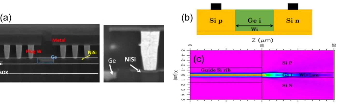
Figure 1a shows a SEM cross-section of the Si/Ge/Si heterojunction photodiode and of the plug landing on the NiSi layer for this device fabricated in 200mm Leti’s 200 mm cleanroom. The width of the Ge layers varied from 300nm to 1 µm. Figure 1c shows a simulation of light propagating from a Si waveguide into such a germanium photodetector. The use of SiGeSi heterojunction enables a better light confinement into the Ge layer than a full Ge integration [5,6]. Indeed, due to the refractive index difference between Si and Ge, the light coupled into Ge does not spread out. Extra optical loss into doped contacts is then reduced, leading to improved responsivity of the photodetectors.
Fig. 1: (a) Cross-sectional SEM image of a fabricated Si/Ge/Si heterojunction based diode, (b) Schematic view of the diode. Wi is the intrinsic width of the diode. (c) Simulation of light propagation from a Si waveguide into a Ge
layer surrounded by N-type and P-type Si contact regions.
3. Results
The dark current-voltage (I-V) characteristics of such waveguide Si/Ge/Si photodetectors were probed. Fig. 2a shows the evolution of the dark current in reverse bias as a function the detector length. Dark currents were lower than 400nA for voltages higher than -4V.
Fig. 2. (a) Dark current as a function of the photodetector length for several reverse bias voltages. (b) Responsivity as a function of the reverse bias voltage for several photodetector lengths.
Fig. 2b shows the evolution of the responsivity with the device length and the reverse bias at a wavelength of 1.55µm. The longer the photodetector and, to a lesser extent, the higher the voltage are, the higher the responsivity is. A maximum responsivity of 1.1 A/W, close to the theoretical limit, was achieved for a device length of 40µm. We can also notice that the responsivity at 0V was quite low. It reaches a sort of plateau for reverse bias voltages higher than -1V. Such a behavior is mainly due to the energy potential barrier at the Si/Ge heterojunction which reduces the electric field at 0V.
The -3 dB bandwidth was determined using a classical RF experiment set-up. A linearly TE polarized light beam at a wavelength of 1.55 µm was coupled into the waveguide. The integrated photodetector was biased using microwave probes up to 50GHz and the optical responses were measured using a lightwave component analyzer. Optical bandwidths higher than 50GHz were obtained for all waveguide Si/Ge/Si photodetectors allowing 40Gbit/s operation in the 1.3µm - 1.55µm wavelength range.
Ge NiSi BOX Metal-Plug W Si Metal BOX Ge Plug W (a) (b) NiSi Ge (c)
(b)
(a)
(c)
3. Conclusions
A new and efficient waveguide Si/Ge/Si photodetector fabrication scheme was proposed that eases device integration into the silicon platform thanks notably to the use of the same doping levels and silicide steps for photo-detectors and modulators. The advantages compared to conventional pure Germanium devices are: cost reduction, better responsivity, improved access resistance and process robustness. State of the art characteristics were obtained in terms of dark current, responsivity, and bandwidth.
In order to increase the sensitivity of photodetectors and reduce the overall power consumption of the optical link, such Si/Ge/Si heterojunction based photodetectors were operated in the avalanche mode. Gains were evidenced, in line with previous results for full waveguide Ge pin detectors [10].
Acknowledgement: The research leading to these results has received funding from the European Community's
Seventh Framework Program (FP7/2007-2013) under grant agreement n° 318178-PLAT4M an the European Research Council (ERC) un- der the European Union’s Horizon 2020 research and innovation program (ERC POPSTAR - grant agreement No 647342).
References:
[1] D. Thomson et al. Roadmap on silicon photonics, J. of Optics 073003 (7), 2016
[2] Sun, C. et al. Single-chip microprocessor that communicates directly using light, Nature 528, 534–538 (2015) [3] Handbook of Silicon Photonics (eds Vivien, L. & Pavesi, L.) (CRC Press, 2013)
[4] JW. Silverstone et al., Silicon quantum photonics, IEEE J. Selected Topics in Quant. Elect. 22(6), 6700113 (2016) [5] L. Vivien, et al. Zero-bias 40Gbit/s germanium waveguide photodetector on silicon. Opt. Express 20, 1096–101 (2012).
[6] L. Vivien, et al. 42 GHz p.i.n Germanium photodetector integrated in a silicon-on-insulator waveguide. Opt. Express 17, 6252–7 (2009). [7] T. Yin, et al. 31 GHz Ge n-i-p waveguide photodetectors on Silicon-on-Insulator substrate. Opt. Express 15, 13965 (2007).
[8] T. Torikai, et al. 40-Gbps high-sensitive waveguide photodetectors. 6020, 602024–602024–8 (2005).
[9] C.T. DeRose, et al. Ultra compact 45 GHz CMOS compatible Germanium waveguide photodiode with low dark current. Opt. Express 19, 24897–904 (2011).