Automation of Electrostatic Material Property Measurement Procedures
by
Alicia M. Volpicelli
Submitted to the Department of Electrical Engineering and Computer Science
in Partial Fulfillment of the Requirements for the Degrees of
Bachelor of Science in Computer Science and Electrical Engineering and Master of Engineering in Electrical Engineering and Computer Science
at the Massachusetts Institute of Technology
February 2, 2000
© 2000 Alicia M.Volpicelli. All rights reserved.
The author hereby grants to M.I.T. permission to reproduce and distribute publicly paper and electronic copies of this thesis
and to grant others the right to do so. MASSACHUSETTS INSTITUTE OF TECHNOLOGY
JUL 2 7 2000
LIBRARIES Author
Department of Electrical hilgineering and Computer Science February 2, 2000
Certified by
Stepen D. Senturia, Barton L. Weller Professor Department of Electrical Engineering and Computer Science Thesis Supervisor
Accepted by
Arthur C. Smith Chairman, Department Committee on Graduate Theses
Automation of Electrostatic Material Property Measurement Procedures
by
Alicia Marina Volpicelli
Submitted to the
Department of Electrical Engineering and Computer Science
February 2, 2000
In Partial Fulfillment of the Requirements for the Degrees of
Bachelor of Science in Electrical Engineering and Computer Science and Master of Engineering in Electrical Engineering and Computer Science
ABSTRACT
The design of released microstructures depends on accurate knowledge of residual stresses and associated elastic constants. The MIT-developed material test procedure, M-Test, uses the variation of pull-in voltage with beam length to extract residual stress and elastic modulus from in-situ test structures. This thesis reports a fully automated computer-microvision procedure that automatically detects electrostatic pull-in and records the pull-in voltage of a full array of beams of different lengths, facilitating the measurement of elastic properties of microstructures. The method is now fully suitable for automatic test equipment in a manufacturing environment and thus brings M-Test to a new level of utility.
Thesis Supervisor: Stephen D. Senturia
Title: Barton L. Weller Professor of Electrical Engineering and Computer Science
Acknowledgments
I would like to take this opportunity to thank the many individuals who have been
instrumental in making my experience at M.I.T. a success. My research advisor, Steve
Senturia, has been pivotal in my academic growth. His expert guidance has encouraged
me to strive for more than I had imagined, and showed me how to apply what I have
already learned. Steve has given me the opportunity to work in this field both technically
and financially.
I had the pleasure to share my office, 39-667, with Erik Deutsch, who helped me
learn about the M-Test procedure and MEMS. Also joining us was our UROP, Raj Sood, who deserves special thanks for conducting some of the M-Test measurements reported
in this thesis.
I would also like to thank Mike "Frank" Rohan for giving me technical and social
support during the preparation of this thesis. My friends and housemates, Gabe
Volpicelli, Manon Whittlesey, Leila Roy, and Robert "Bubba" Leff helped me maintain
sanity and enjoy my time at M.I.T.
Finally, I would like to thank my parents for their never ending love and support.
This work was sponsored, in part, by DARPA under contract N6601-97-C-8620.
Table of Contents
CHAPTER 1: INTRODUCTION... 7 1.1 T H ESIS O U TLIN E ... 8 1.2 M OTIVATION... 8 1.3 M -TEST PROCEDURE... 9 1.4 TEST STRUCTURES ... 12CHAPTER 2: AUTOMATION OF THE M-TEST PROCEDURE ... 15
2.1 M ETHODS OF PULL-IN DETECTION ... 15
2.2 AUTOMATION SYSTEM: NOMARSKI OPTICS ... 16
2.3 PULL-IN DETECTION: NOMARSKI OPTICS... 17
2.4 CANTILEVER PULL-IN DETECTION ... 18
2.5 AUTOMATION SYSTEM: BEAM CONTACT... 19
2.6 PULL-IN DETECTION: BEAM CONTACT ... 20
2.7 GRAPHICAL USER INTERFACE ... 20
CHAPTER 3: SYSTEM CAPABILITIES ... 22
3.1 ACCURACY/PRECISION ... 22 3.2 ERROR ANALYSIS ... 22 3 .3 S P E E D ... 2 3 CHAPTER 4: RESULTS ... 25 4.1 ALGORITHM RESULTS ... 25 4.2 REPEATABILITY TESTS ... 26 4.3 M UM PS RESULTS ... 27 4.4 POLYCHROMATOR BACKGROUND... 30
4.5 POLYCHROMATOR M -TEST RESULTS... 30
CHAPTER 5: CONCLUSIONS ... 33
REFERENCES... 34
List of Figures
FIGURE 1.1: SCHEMATIC OF THE PULL-IN EFFECT... 9
FIGURE 1.2: DEFLECTION VS. VOLTAGE FOR THE PULL-IN PHENOMENON... 10
FIGURE 1.3: THE M-TEST APPROACH (T = THICKNESS, Go = GAP, L = BEAM LENGTH)... 1 1 FIGURE 1.4: M U M PS BEAM ... 13
FIGURE 1.5: A RRAY OF TEST STRUCTURES... 13
FIGURE 1.6: POLYCHROM ATOR BEAM ... 14
FIGURE 1.7: BEAM-CONTACT CROSS-SECTION. ... 14
FIGURE 2.1: N O M ARSKI OPTICS. ... 15
FIGURE 2.2: INTERFERENCE FRINGES ... 16
FIGURE 2.3: A UTOM ATION SYSTEM . ... 17
FIGURE 2.4A : POLYSILICON BEAM ... 17
FIGURE 2.4B: FRAME BEFORE PULL-IN IS DETECTED... 18
FIGURE 2.4C: FRAME AFTER PULL-IN IS DETECTED... 18
FIGURE 2.5: DOUBLY-SUPPORTED BEAM REGIONS OF INTEREST. ... 18
FIGURE 2.6: CANTILEVER REGIONS OF INTEREST. ... 18
FIGURE 2.7A : C ANTILEVER BEAM . ... 19
FIGURE 2.7B: FRAME BEFORE PULL-IN IS DETECTED... 19
FIGURE 2.7C: FRAME AFTER PULL-IN IS DETECTED... 19
FIGURE 2.8: BEAM -CONTACT SETUP. ... 19
FIGURE 2.9: G RAPHICAL U SER INTERFACE... 21
FIGURE 4.1: INTENSITY VS. VOLTAGE FOR REGIONS OF INTEREST. ... 26
FIGURE 4.2: HISTOGRAM OF 100 MANUAL AND AUTOMATIC PULL-IN TESTS... 27
FIGURE 4.3: H ISTOGRAM OF RESULTS... 28
FIGURE 4.4: PULL-IN VOLTAGE VS. BEAM LENGTH FOR MUMPS RUN 14. ... 29
FIGURE 4.5: PULL-IN VOLTAGE VS. BEAM LENGTH FOR ENTIRE DATA SET... 31
FIGURE 4.6: PULL-IN VOLTAGE VS. BEAM LENGTH FOR LIMITED DATA SET... 32
List of Figures
5
List of Tables
TABLE 1.1: NUMERICAL CONSTANTS IN EQUATION 1.1 FOR DOUBLY-SUPPORTED BEAMS. 12
TABLE 4.1: RESULTS FROM 100 MANUAL AND AUTOMATIC PULL-IN TESTS... 26
TABLE 4.2: REPEATABILITY DATA USING THE AUTOMATED SYSTEM... 27
TABLE 4.1: M UM PS RUN 14 TEST RESULTS... 29
TABLE 4.2: COMPARISON OF AUTOMATIC AND MANUAL RESULTS. ... 30
TABLE 4.4: POLYCHROMATOR TEST RESULTS FOR ENTIRE DATA SET. ... 31
TABLE 4.5: POLYCHROMATOR TEST RESULTS FOR LIMITED DATA SET... 32
List of Tables
6
CHAPTER 1
Introduction
As the commercial demand for microelectromechanical systems used for mechanical sensors and actuators increases, methods of characterization and analysis are needed for the successful design and modeling of these devices. The design of released
microstructures depends on accurate knowledge of residual stresses and associated elastic constants. The accurate measurement of these quantities is the topic of this thesis. The MIT-developed material test procedure, M-Test, enables process monitoring of
uniformity and repeatability, and the extraction of mechanical properties [1-5]. This is accomplished by in-situ measurements of an electromechanical instability point, which is achieved by electrostatic actuation with a voltage called the pull-in voltage, V, .The M-Test Procedure uses the variation of pull-in voltage with beam length to extract the residual stress and elastic modulus of the actuated material.
This thesis presents a fully automated computer-microvision procedure that detects electrostatic pull-in, facilitating the measurement of elastic properties of microstructures. The system automatically detects the pull-in event and records the pull-in voltage of a full array of beams of different lengths.
Chapter 1: Introduction
7
1.1
Thesis Outline
The motivation and goals for this thesis, and its purpose of facilitating data acquisition for the M-Test procedure, are discussed in Chapter 1. In addition a brief outline of the
M-Test procedure and the devices used is presented. In Chapter 2, the automation of the M-Test procedure is presented. The setup of the automation system is outlined, and the algorithms that detect the pull-in event are described. Finally, the development of the user-friendly interface is discussed. In Chapter 3 system capabilities including accuracy, precision, and speed are discussed. In Chapter 4 the results from using this new system are presented. In Chapter 5 conclusions are drawn about the automation system, and its function in material property extraction.
1.2 Motivation
M-Test data can be used to monitor process repeatability and uniformity and calculate material properties. Manual M-Test data acquisition, however, is slow and cumbersome. The manual detection of pull-in is also prone to inaccuracy. Automation of the M-Test procedure has been shown to improve accuracy and facilitate large quantities of data acquisition with minimal user interaction.
Chapter 1: Introduction
8
1.3 M-Test Procedure
The M-Test procedure enables the extraction of the material properties, k (elastic modulus) and & (axial residual stress), by measuring the pull-in voltage for a series of test structures of different lengths. Mathematical models are used to determine the
bending parameter, B, and stress parameter, S, of the material. With accurate metrology of the test structures, the desired material properties can be determined.
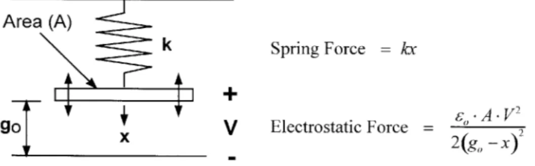
Area (A) k Spring Force = kx 0 1+ go
V
Electrostatic Force = " 2 ___ ___ ___ ___ __2(g ___ 0 xFigure 1.1: Schematic of the pull-in effect.
The M-Test procedure requires the measurement of an electromechanical
instability point called the pull-in voltage. A lumped one-dimensional model of electrostatic pull-in is shown in Figure 1.1. The pull-in effect is modeled as a parallel-plate capacitor with one fixed parallel-plate and one parallel-plate attached to a fixed surface by a spring.
A DC voltage is applied, causing an electrostatic force between the two plates. The
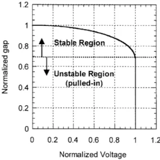
restoring force of the beam is modeled as a spring with a spring coefficient k. The displacement versus voltage characteristic is shown in Figure 1.2. When actuated by a low voltage, the beam undergoes a stable deflection. Stable equilibrium is maintained as the voltage is increased until the beam has displaced one-third to one half
Chapter 1: Introduction
9
the free-space gap, depending on the beam thickness and residual stress [6]. At this point, called the pull-in voltage, the beam deforms and travels the remaining distance, snapping
to the underlying electrode. This model is limited to simple beam geometry with rigid
supports; it is not as effective for beams with compliant supports, stress that varies
through the beam thickness, or other unknown stress dependencies.
1.2 Q_ 0.8 - Stabl Region a > . . CU 0.6 CU Unstable Rpgion o-. (pulled-in)-0 .2 --- -- - - - -- - -0 0 0.2 0.4 0.6 0.8 1 1.2 Normalized Voltage
Figure 1.2: Deflection vs. voltage for the pull-in phenomenon.
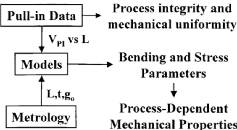
The M-Test approach (Figure 1.3) uses pull-in voltage measurements of test structures that contain doubly-supported beams of varying length. Mathematical models are used to determine bending and stress parameters, which are used to characterize process uniformity and repeatability. With accurate metrology, elastic modulus, F, and the axial residual stress, 8 , can be extracted.
Chapter 1: Introduction
10
- DProcess
integrity and
mechanical uniformity
VP vs L
Bending and Stress
Parameters
L,t,g
0MProcess-Dependent
Mechanical Properties
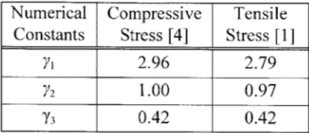
Figure 1.3: The M-Test Approach (t = thickness, go = gap, L = beam length). Pull-in voltage measurements taken as a function of doubly-supported beam length are used by M-Test models (Equation 1.1) [2] to determine the bending parameter,
B, and stress parameter, S . Equation 1.1 gives V,, as a function of L , B, and S. The
variables w , t and go are the measured geometric values of device width, thickness and
initial gap. The values for the numerical constants 7, , 72, and /3 in Equation 1.1 are
shown in Table 1. The data of pull-in voltage versus beam length is fit to Equation 1.1, using the Levenberg-Marquardt curve-fitting algorithm, to extract the B and S parameters.
VI (1.1) L2 2 -- cosh(/2 '- (3 -S)/ B -L) 7 2 -(3 S)/B -L -sinh(7 2 -T(3- S)IB -L) S= B 3 (1.2) t .g,, t - V) = 3 (1.3)
The B and S parameters can be used as a measure of mechanical process uniformity, as they are a product of device geometry and mechanical properties. In
Chapter 1: Introduction
11
addition, the B and S parameters can be used with accurate metrology to extract the material properties of the system. E, which is obtained from Equation 1.2, is equal to the Young's Modulus E for slender beams, and approaches the plate modulus E/(1 - v2) for wide beams [3,4], where v is the Poisson ratio of the actuated material. & is obtained from Equation 1.3, where o0 is the biaxial residual stress.
Numerical Compressive Tensile
Constants Stress [4] Stress [1]
A 2.96 2.79
Y2 1.00 0.97
73 0.42 0.42
Table 1.1: Numerical constants in Equation 1.1 for doubly-supported beams. A major advantage of the M-Test technique is that it can be performed at the
wafer level using standard electronic test equipment and a microscope. The analytical models to extract B and S based on the measured pull-in voltages are developed and discussed extensively by Gupta [2,4], based on the work of Osterberg [1,3]. Methods for accurate geometry measurements are discussed in Deutsch [5].
1.4 Test Structures
One set of samples were fabricated by the Microelectronics Center of North Carolina
(MCNC) using the Multi-User MEMS Process (MUMPs) [12]. A cross-section of the
MUMPs doubly-supported beam is shown in Figure 1.4. The MUMPs structures contain three layers of low-pressure chemical vapor deposition (LPCVD) polysilicon deposited at 5800C, layers of phosphosilicate glass (PSG), and an insulating nitride layer that is
deposited on the entire wafer. For this structure the first layer of polysilicon (Poly-0) is
not used. A support region is etched in the first layer of oxide (PSG-0), where the
conformal deposition of the second polysilicon layer (Poly-1) forms beams after
patterning. The second oxide (PSG-1) is etched to form contact regions for the third layer
of polysilicon (Poly-2). Finally, metal is deposited on Poly-2 to form contact pads. A
sacrificial etch of concentrated HF removes the PSG, releasing the devices.
l NITRIDE M POLYSILICON PAD METAL
Figure 1.4: MUMPs beam.
A second set of samples, designed for use with automated test equipment, was
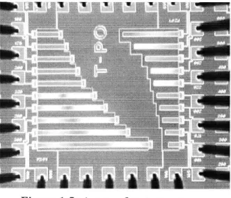
fabricated at Honeywell Technology Center as part of a joint endeavor between M.I.T., Honeywell, and Sandia National Labs called the Polychromator project [13]. Five die on
each polychromator wafer contain sets of beams of varying geometries for the M-Test
procedure, with pads arranged to facilitate probe card contact (Figure 1.5).
Figure 1.5: Array of test structures.
Chapter 1: Introduction
13
Figure 1.6 shows the cross-section of the polychromator test structure. An insulating layer of silicon nitride is deposited over the entire wafer. A layer of LPCVD polysilicon (Poly-0) is deposited, forming an electrical interconnect between the contact pad and the grounding electrode. A second nitride layer insulates the grounding electrode
from the actuated beam so that pull-in does not create a short. A second layer of polysilicon, (Poly-1) is deposited forming an interconnect between the beam and the actuation contact pad. A third layer of polysilicon, (Poly-2) is deposited on a sacrificial
low-temperature-oxide (LTO-0), where stiffer support regions have been formed by trapping the oxide. The LTO-0 layer is removed via a sacrificial etch of HF, releasing the devices.
D NITRIDE POLYSILICON O OXIDE PAD METAL
Figure 1.6: Polychromator beam.
Figure 1.7 shows the cross-section of another polychromator test structure. The second layer of polysilicon (Poly-1) is deposited over the insulating silicon nitride, forming an interconnect to the underlying electrode. When pull-in occurs, a short is created that can be electrically detected.
E NITRIDE E POLYSILICON [ OXIDE
*
PAD METALFigure 1.7: Beam-contact cross-section.
Chapter 1: Introduction
14
CHAPTER 2
Automation of the M-Test Procedure
In order to extract mechanical properties and assess die to die, wafer to wafer, and lot to
lot variations, accurate pull-in voltage measurements of test structures consisting of doubly-supported beams of varying length are required. The automation of data acquisition procedures can be realized by the analysis of video images from an optical microscope. In this chapter a microvision system is described that automatically acquires accurate pull-in data, facilitating the extraction of mechanical properties.
2.1 Methods of Pull-in Detection
There are a number of methods to detect pull-in; optical methods using Nomarski optics, optical methods using interference fringes, and electrical methods. The Nomarski setup uses a monochrome camera which provides a grayscale indication of the magnitude of the slope of the bending beam. Figure 2.1 shows a pulled in beam. The sides of the beam are in white since these are the areas with the greatest slope. The middle is dark since it is flush against the surface of the wafer.
Figure 2.1: Nomarski optics.
Chapter 2: M-Test Automation
15
Interference fringes indicate a difference in height of half a wavelength of light, or around 273nm. Figure 2.2 shows a beam with interference fringes; there are about 7.5
fringes on each side of the beam, indicating a change in height of 2tm. Since the free-space gap of the device is 2ptm, the beam is pulled in.
Figure 2.2: Interference fringes.
Electrical methods for detecting pull-in use either the contact of the beam against the underlying electrode or the detection of the capacitance change that occurs with the
lowering beam. A cross-section of the beam contact test structure is shown in Figure 1.7. The collapsing beam creates a short that can be electrically detected.
The easiest to automate of these three methods are the beam contact and
Nomarski optics methods, which are the methods selected for automation. Algorithms are described in the following sections which accomplish both methods of detection
automatically.
2.2
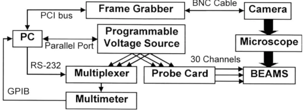
Automation System: Nomarski Optics
Figure 2.3 shows the setup of the automation system. A full array of beams is viewed with a microscope, imaged with a CCD camera, and sequentially actuated by a multi-channel programmable voltage source using a probe card. A computer microvision algorithm, described below, determines whether the test structure being actuated has reached the instability point. In order to provide an accurate measurement, a precision
multimeter is used to determine the voltage on a given beam for each frame, using a multiplexer that is controlled by the PC. The setup could also be configured with a single-channel voltage source, and a demultiplexer attached to the probe card. The voltage source used should be capable of high voltages, since beams of 200um in length take on the order of 100 volts to pull-in.
Multiplexer Probe C C BEAMS
GPIB +
Multimeter
Figure 2.3: Automation system.
2.3 Pull-in Detection: Nomarski Optics
The pull-in event is detected by the sharp change in optical intensity when viewed with Nomarski optics (Figure 2.4). Figure 2.4A shows a polysilicon beam without voltage applied, Figure 2.4B shows the beam one frame prior to the pull-in event, and
Figure 2.4C shows the beam one frame after the pull-in event. This change is automatically detected by this algorithm.
Figure 2.4A: Polysilicon beam.
Chapter 2: M- Test Automation 17
Figure 2.4B: Frame before pull-in is detected.
Figure 2.4C: Frame after pull-in is detected.
Figure 2.5 shows in outline the "regions of interest" that are used to detect pull-in.
A slow ramping of voltage creates a small change in intensity from frame to frame in
each area. When pull-in occurs, a dramatic change in the intensity occurs, which is detected by comparing sequential frames. Each area's intensity is computed by averaging the value of the pixels in the area. This average is then compared to the average value of the same area from the previous frame. Pull-in is detected if there is a large change from frame to frame in one or more of the six regions.
Figure 2.5: Doubly-supported beam regions of interest.
Figure 2.6: Cantilever regions of interest.
2.4 Cantilever Pull-in Detection
Cantilever beams can also be used by this system. Cantilever beams also undergo a distinct change when viewed with Nomarski optics during pull-in. However, different
Chapter 2: M-Test Automation
18
regions of interest are used. Figure 2.6 shows the regions of interest used for cantilever beams. Figures 2.7A-C show the change that can be automatically detected when a cantilever beam is pulled in.
Figure 2.7A: Cantilever beam.
Figure 2.7B: Frame before pull-in is detected.
Figure 2.7C: Frame after pull-in is detected.
2.5
Automation System: Beam Contact
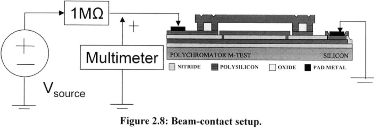
The setup for this system is shown in Figure 2.8. A voltage divider is created by placing a large resistor in series with the test structure. A voltage source steps the voltage while the multimeter monitors the voltage divider.
Multimeter
d ; F] ~NITRIDE MPOLYSILICON OOXIDE MPAD METAL
Vsource
Figure 2.8: Beam-contact setup.
2.6 Pull-in Detection: Beam Contact
With beams that are fabricated as in Figure 1.7, it is possible to detect pull-in electrically. The beam snapping to the underlying grounded electrode shorts the circuit. Before pull-in, the multimeter voltage will match the source voltage. At pull-in the circuit becomes a voltage divider between a 1 M Q resistor and the contact resistance of the polysilicon beam. The program raises the source voltage while watching the multimeter voltage. As soon as the multimeter voltage drops by a large amount, the voltage that was applied is recorded as the pull-in voltage.
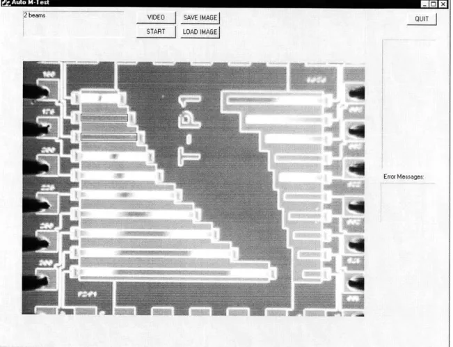
2.7 Graphical User Interface
To enable easy control of the program a Visual C++ interface was created. Beams are selected by mouse click, and then highlighted in red. Clicking a beam again results in unselecting the beam. Pop-up menus let the user choose whether beams or cantilevers are being tested, the starting voltage for the first beam, the voltage step between frame checks, the file to save results in, and whether the system is in probe card or single probe configuration. If a probe card is being used, the user selects a mapping file that maps the voltage channel to a particular beam length. Thus, beams must all be of different lengths. Beams to be tested that were selected by mouse input are sorted in order of length. The longest beams are tested first because the large voltages needed to pull in the short beams can charge the nitride layer, affecting the pull-in voltages. Actuating the beams in this order also accelerates the testing process, since the pull-in voltage of the previous beam is
used to indicate a starting point for the next beam, so that the total time to test a full array of beams is on the order of the time to test the shortest beam. During testing, the display shows how many beams are selected, what the length and voltage of the current beam being tested is, and the pull-in results of the beams previously tested.
&Auto M-TestMO
2 beams VIDEO SAVE IMAGE
QUIT
START ILAD IMAGE
Error Messages
...~ ANA
Figure 2.9: Graphical User Interface.
Chapter 2: M-Test Automation 21
CHAPTER 3
System Capabilities
3.1 Accuracy/Precision
The accuracy of the pull-in detection system is dependent on the calibrated precision
multimeter that is used in the setup. The precision of the system is controlled by the voltage step that is set by the user. After a frame of video is compared with the previous frame, and pull-in is not detected, the voltage is raised by the voltage step, and then another frame of video is grabbed for analysis. When a frame of video indicates that pull-in has occurred, an accurate voltage is read from the multimeter, but since the video frame is only checked once after each voltage step, the precision of the pull-in voltage measurment is limited by size of the voltage step.
3.2 Error Analysis
An error analysis of the M-Test Approach is discussed in detail in Gupta [4]. Using his formula, one can determine how the error in each measurement contributes to the error in the value for the elastic modulus, F. An approximate RMS analysis of the M-Test equation (Equation 1.1) yields equations 3.1 and 3.2, assuming that the contributing errors are normally distributed and independent.
SE SV SL St
~E 2. '3' +4 3 3 50 (3.1)
E V, L t go
4.(' ) +16- ) +9- 7 +9- 7g (3.2)
Ek Vill L t go,
The probable error in the profilometer measurements of t and go is estimated to be 0.7%
[5], contributing ~ 3% to the error in E. The metrology measurement error for L is negligible since the lengths of the beams are all in the range of 200-1000pjm. In order to minimize the error contributed by the measurement of Vl, , a small voltage step must be used. However, a larger voltage step speeds up the voltage measurement. The lowest pull-in voltages of the MUMPs and Polychromator devices are just under 10 volts, indicating that a voltage step of 0.025 volts, the minimum step of the voltage source in the setup, contributes a maximum of 0.04% to the error to F. If a faster measurement is
required, the error contributed by the voltage measurement remains small compared to the geometry error. Using a voltage step of 0.13 volts would contribute ~1% error to the error in E, and doubles the speed of the measurement.
3.3 Speed
The speed of the system is also controlled by the user. The system does not begin analyzing each frame until it is within 20% of the values estimated by a file that the user inputs. Without estimated values, the system does not begin analyzing each frame until it reaches the pull-in voltage of the previous beam tested, since they are tested in order of
Chapter3: System Capabilities
23
length, and shorter beams have higher pull-in voltages. For each beam, the voltage is ramped to near the estimated value, at about 2 volts/sec, and when the frames are being analyzed, the voltage increases at about 0.2 volts/sec. If the values are very close to the actual pull-in voltages, and if a voltage step of .025 is used, an array of ten beams with pull-in voltages ranging from 5 volts to about 100 volts can be tested within 10 minutes.
Chapter3: System Capabilities
24
CHAPTER 4
Results
The M-Test automation system is being used in a variety of applications for
multiple projects, and so results from various test structures are reported. The M-Test procedure requires the automation system to acquire large amounts of data from test devices in order to perfect the model used in the extraction of material properties. The Polychromator project uses the automation system to aid in the monitoring of the stress of a microelectromechanical device. Presented in this chapter are the results of the
algorithm, results from the testing of MUMPs structures, a comparison to manual testing, and some of the initial Polychromator test results.
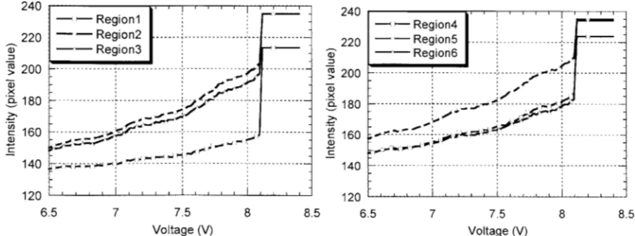
4.1 Algorithm Results
Figure 4.1 shows intensity vs. voltage for a sample MUMPs beam. The left graph shows the left regions of interest, and the right side shows the right regions of interest. As the voltage increases, the intensity of the six regions of interest slowly increase. When the pull-in voltage is reached, the intensities of the six regions increase by a much larger amount, which is detected by the program.
Chapter 4: Results
25
240 - Region1 240 -- Region4 220 -- - Region2 . 220 -- Region5 200 - - ---- --- --- -- - -- - 200 --22180 -- -- -- - --- -- - 18 0 ---6.5 7 7.5 8 8.5 6.5 7 7.5 8 8.5 Voltage (V) Voltage (V)
Figure 4.1 Intensity vs voltage for regions of interest.
4.2 Repeatability Tests
The automation program enables more efficient and precise repeatability testing. The human eye cannot detect pull-in as fast as the computer, and as a result, pull-in voltages are consistently higher when taken manually, and span a larger range of values. 100
pull-in voltages were taken for one 500pm Polychromator beam-contact test structure manually and using the automated system. A standard deviation of 0.025 volts is
expected, since that is the voltage step that is used. Other random errors lead to a standard
deviation of 0.032 volts for the automated system. Manual testing yields a 0.086 volt standard deviation. The difference between manual and automatic testing is shown in Table 4.1. Figure 4.2 shows the histogram of the two sets of data.
Testing Ave rage Pull-in Standard
Method
j
Voltage DeviationManual 11.87 .031667 Automatic
j12.029
.085548Table 4.1: Results from 100 manual and automatic pull-in tests.
Cha te 4:--- Res lt --- 26---
0-0 35 30 25 20 15 10 5 U 11.7 11.8 11.9 12 12.1 12.2 12 Range (V)
Figure 4.2: Histogram of 100 manual and automatic pull-in tests.
.3
Tests were also repeated on beams of various lengths. Each beam was tested ten times. The standard deviation for all the beams is close to the error based on the program's step voltage, 0.025 volts (Table 4.2).
Beam Average Pull-in Standard
Length Voltage Deviation
700tm 6.9472 .018531
600tm 8.9259 .017416
500tm 11.882 .024335
400ptm 17.56 .023298
300tm 30.341 .016281
Repeatability data using the automated system.
4.3 MUMPs Results
Prior to M-Test automation, manual tests were performed to extract the material
properties of 23 different MUMPs die consisting of five runs, with between two and six
- --- --- ------- ---' 1 -Table 4.2: 27 Manual ---- --- -- Autom atic -- -- - ---- -- ---- --- --- --- ---- --- -- ---- ----- -- ---- ---x-- -> X Chapter 4: Results
die per run (Figure 4.3) [11]. The average elastic modulus was found to be 155±5 GPa.
This is 5% below the theoretical elastic modulus for randomly oriented grain
polysilicon [7]. The grain orientation of the polysilicon will significantly affect the elastic
modulus, so this comparison can only be used as an estimate of the expected value.
Elastic modulus extraction based on tensile testing of MUMPs specimens by Sharpe [8]
yield a systematically higher modulus of 169±6 GPa, 9% above the value reported here.
The origin of this discrepency has not yet been identified. It suggests there may be small
residual modeling errors or measurement errors in the M-Test procedure, and is being
investigated. 10 . . MUMPs5 E MUMPs 16 8 - MUMPs 14 aD E MUMPs9 El MUMPs 15 4 6 -0 E 4 I z 2 135 140 145 150 155 160 165 170 175 Elastic Modulus (GPa)
Figure 4.3: Histogram of results.
To test the automation program, pull-in voltages were taken of MUMPs run 14
test structures. The structures used were those shown in Figure 1.4. The data points were
fit to the M-Test equation (Equation 1.1) using KaleidaGraph [14], which uses the
Levenberg-Marquardt curve-fitting algorithm. The curve fit for the six die is shown in
Figure 4.4. Extraction of material properties from automated testing resulted in an average elastic modulus of 156±3 GPa and an average axial residual stress of
4.9±0.3 MPa, as shown in Table 4.1. The voltages recorded automatically are consistently
lower than the voltages recorded manually, as seen in the repeatability testing. However, the difference in pull-in voltage from manual testing is not significant enough to create a
large difference in the extracted values. The elastic modulus measurements were within
2% and residual stress measurements were within 9% of the values measured in the initial
testing (Table 4.2). The standard deviation for the previously reported results, referring to
the variation in material property from die to die within a process run, was found to be
1.6% for the elastic modulus, and 3.0% for the residual stress [5]. The values reported
here have a similar distribution, with a standard deviation of 1.3% for elastic modulus
and 3.4% for the residual stress.
80 - Die 1 7 --- --- --- --- - -- - - 0 _ i 70 - Die 2 Die34 ~6 0 - --- ---- -- x -- D ie 4 e, 50 --- -- --- --- --- --- --- - D ie 5 Die 6 40 --- - --- --- ---3 0 -- - -- -- -- --- -- -- --- - - - - -2 0 - -- ---- - - ---- ---- --- -- - ---- --- --- ---- ----- ------ ---1 - -- - - ---- -- --- - ---- --- -- --- -- --- -- -- ---20 '---'---'-20 100 200 300 400 500 600 700 Beam Length ( tm)
Figure 4.4: Pull-in voltage vs. beam length for MUMPs run 14.
Die B (Pa*m6) S (Pa*m4) t (tm) g (pIm)
j
(GPa) 6' (MPa)1 9.OE-24 6.73E-17 2.01 1.92 156.52 4.73 2 9.3E-24 6.99E-17 2.04 1.90 159.69 4.99 3 8.02E-24 5.75E-17 2.02 1.83 158.69 4.64 4 8.35E-24 6.51E-17 2.01 1.88 154.80 4.87 5 9.33E-24 7.25E-17 2.01 1.94 157.35 4.94 6 8.72E-24 6.80E-17 2.05 1.87 154.74 5.07
Table 4.1: MUMPs run 14 test results.
Die F(GPa) F(GPa) Deviation 8(MPa) 8(MPa) Deviation
Automatic Manual Automatic Manual
1 156.52 156.6 0.9% 4.73 5.2 9.0% 2 159.69 158.0 1.1% 4.99 5.1 2.1% 3 158.69 158.5 0.1% 4.64 5.0 7.2% 4 154.80 155.1 0.2% 4.87 4.8 1.5% 5 157.35 160.2 1.8% 4.94 5.1 3.1% 6 154.74 153.3 0.9% 5.07 5.1 0.5%
Table 4.2: Comparison of automatic and manual results.
4.4
Polychromator Background
The Polychromator project is a joint endeavor between Honeywell, Sandia, and M.I.T. The device is a MEMS-based optical diffraction grating with a large number of
individually controllable micromirror grating elements which can be electrically
programmed to reproduce spectral features of target chemical species [9,10]. In order to assess process uniformity, repeatability, and to determine the resulting material properties of the polysilicon in the process, each test wafer has M-Test structures that are tested and analyzed.
4.5
Polychromator M-Test Results
Many different types of beams are tested for the Polychromator project; standard
(Figure 1.6), and beam contact (Figure 2.3). The curve fit for the various pull-in tests are shown in Figure 4.5. The results for the various test structures are shown in Table 4.4.
Chapter 4: Results
30
80
80-- PoIy2 Standard
70 --- - --- ~ ---- --- -- o - PoIy2 Beam Contact
1 0 -- --- -- -- --- --- - - -- - -- --- - - - -0' o 40 20 10 --- --- - ---0 0 200 400 600 800 1000 Beam Length (tm)
Figure 4.5: Pull-in voltage vs. beam length for entire data set.
Polysilicon gD t)tGm B S k Ga
(M )
Layer
J~g(a)
t(a) (Pa*m') (Pa*m') E(Ga &(M )PSty2dBeaStandBad Pol2 2.64 1.25 5.81E-24 3.53E-17 186.53 1.66431
Bam 2.53 1.25 5.81E-24 3.53E-17 183.71 1.7431
Contact
Table 4.4: Polychromator test results for entire data set.
Extraction of material properties from this data results in a higher elastic modulus than expected. Due to fabrication differences between the polychromator test structures and the MUMPs test structures, the effective electrode length has not yet been
determined, and thus the model is not accurate enough to obtain the correct values for elastic modulus and the residual stress. Using a data set limited to higher values of beam length minimizes this modeling error. The curve fit for the various pull-in tests of the limited data set are shown in Figure 4.6. The results for the various test structures are shown in Table 4.5.
Chapter 4: Results
31
20 a) 0 -5 0-15 10 300 Figure 4.6 400 500 600 700 800 900 1i Beam Length ([m)
Pull-in voltage vs. beam length for limited data set.
00
Polysicon g (tm) t (tm) Pm) (Pam 4) (GPa)
- (MPa) Poly2
Standr 2.64 1.25 5.88E-24 3.84E-17 163.6 1.67
Standard
Poly2 Beam 2.53 1.25 4.9E-24 3.53E-17 154.8 1.74
Contact I
Table 4.5: Polychromator test results for limited data set.
Limiting the data set results in elastic modulus and axial residual stress results that are closer to the theoretical value for randomly oriented grain polysilicon. Additional modeling must be performed for these new test structures. Despite this problem the automation system has proven to be more efficient gathering data from these test structures.
Chapter 4: Results
32
--- PoIy2 Standard
- PoIy2 Beam Contact
' -
-5
CHAPTER
5
Conclusions
The design of released micro-structures depends on accurate knowledge of residual
stresses and associated elastic constants. The importance of acquiring large amounts of data in order to accurately and efficiently determine material properties was discussed. The automation of the M-Test procedure and its improvements in pull-in voltage
measurement were presented, the algorithm for the automation system was described, and results from the program were compared to manual testing. Because each video frame is checked before incrementing the applied voltage, the precision is controlled by the program. Typical voltage increments are 25 mV, a level that cannot be achieved
manually. The total time now being used to check an array of ten beams is on the order of ten minutes. With this computer vision system, the M-Test procedure is now fully
compatible with automatic test equipment found in a typical manufacturing environment, and thus brings M-Test to a new level of utility.
Chapter 5: Conclusions
33
References
[1] P. M. Osterberg, and S. D. Senturia, "M-TEST: A Test Chip for MEMS Material
Property Measurement Using Electrostatically Actuated Test Structures" Journal of Micro-electro-mechanical Systems, Vol 6, No. 2, pp. 107-118, June 1997.
[2] R. K. Gupta, P. M. Osterberg, and S. D. Senturia, "Material Property Measurements of Micro-mechanical Polysilicon Beams" Invited Paper, SPIE 1996 Microlithography and Metrology in Micromachining, II, Austin, TX, USA, October 1996, pp 39-45.
[3] P. M. Osterberg, "Electrostatically Actuated Microelectromechanical Test Structures
for Material Property Measurement" Ph.D. Thesis, September 1995, MIT.
[4] R. K. Gupta, "Electrostatic Pull-in Test Structure Design for in-situ Mechanical Property Measurements of Microelectromechanical Systems (MEMS)" Ph.D. Thesis, June 1997, MIT.
[5] E. R. Deutsch, "Development of Calibration Standards for Accurate Measurement of Geometry in Microelectromechanical Systems" M.S. Thesis, June 1998, MIT.
[6] E. Hung, "Positioning, Control, and Dynamics of Electrostatic Actuators for Use in
Optical and RF Systems" Ph.D. Thesis, August 1998, MIT.
[7] G. Simmons and H. Wang, Single Crystal Elastic Constants and Calculated Aggregate
Properties: A Handbook, 2"' Ed., Cambridge, Massachussetts, MIT Press, 1971, pp. 85,
262.
[8] W.N. Sharpe, Jr., B. Yuan, R. Vaidyanathan, and R.L. Edwards, "New Test
Structures and Techniques for Measurement of Mechanical Properties of MEMS
References
34
Materials (Invited Paper)," Proceedings of SPIE 1996 Microlithography and Metrology in Micromachining II, Austin, TX, October 1996, pp. 78-91.
[9] "Synthetic spectra: A Tool for Correlation Spectroscopy," M.B. Sinclair, M.A.
Butler, A.J. Ricco, and S.D. Senturia, Applied Optics 36, pg. 3342-3348, May 20, 1997.
[10] "Synthetic Infrared Spectra," M.B. Sinclair, M.A. Butler, S.H. Kravitz, W.J.
Zubrzycki, and A.J. Ricco, Optics Letters 22, pg. 1036-1038, July 1, 1997.
[11] "Use of Computer Microvision to Automate Electrostatic Material Property Measurement Procedures"A. M. Volpicelli, E. R. Deutsch, and S. D. Senturia,
Transducers '99, pg. 922-923, June 1999.
[12] Devices courtesy of David Kester and Karen Markus at the Microelectronics
Center of North Carolina (MCNC), and fabricated by the Multi-User MEMS Process (MUMPs). http://mems.mcnc.org.
[13] Devices courtesy of David Arch, William Herb, Dan Youngner, Ben Hocker, and Aravind Padmanabhan, at the Honeywell Technology Center.
[14] KaleidaGraph 3.0 (Synergy Software)
References
35