Publisher’s version / Version de l'éditeur:
Applied Physics Letters, 79, 16, pp. 2618-2620, 2001
READ THESE TERMS AND CONDITIONS CAREFULLY BEFORE USING THIS WEBSITE. https://nrc-publications.canada.ca/eng/copyright
Vous avez des questions? Nous pouvons vous aider. Pour communiquer directement avec un auteur, consultez la première page de la revue dans laquelle son article a été publié afin de trouver ses coordonnées. Si vous n’arrivez pas à les repérer, communiquez avec nous à [email protected].
Questions? Contact the NRC Publications Archive team at
[email protected]. If you wish to email the authors directly, please see the first page of the publication for their contact information.
NRC Publications Archive
Archives des publications du CNRC
This publication could be one of several versions: author’s original, accepted manuscript or the publisher’s version. / La version de cette publication peut être l’une des suivantes : la version prépublication de l’auteur, la version acceptée du manuscrit ou la version de l’éditeur.
For the publisher’s version, please access the DOI link below./ Pour consulter la version de l’éditeur, utilisez le lien DOI ci-dessous.
https://doi.org/10.1063/1.1412284
Access and use of this website and the material on it are subject to the Terms and Conditions set forth at
Thermal stability and diffusion in gadolinium silicate gate dielectric
films
Landheer, D.; Wu, X.; Morais, J.; Baumvol, I. J. R.; Pezzi, R. P.; Miotti, L.;
Lennard, W. N.; Kim, J. K.
https://publications-cnrc.canada.ca/fra/droits
L’accès à ce site Web et l’utilisation de son contenu sont assujettis aux conditions présentées dans le site LISEZ CES CONDITIONS ATTENTIVEMENT AVANT D’UTILISER CE SITE WEB.
NRC Publications Record / Notice d'Archives des publications de CNRC:
https://nrc-publications.canada.ca/eng/view/object/?id=6ddd403b-e6c1-483f-a951-6ce626709c51 https://publications-cnrc.canada.ca/fra/voir/objet/?id=6ddd403b-e6c1-483f-a951-6ce626709c51Thermal stability and diffusion in gadolinium silicate gate dielectric films
D. Landheera) and X. WuInstitute for Microstructural Sciences, National Research Council of Canada, Ottawa, Ontario, Canada K1A 0R6
J. Morais, I. J. R. Baumvol, R. P. Pezzi, and L. Miotti
Instituto de Fisica, Universidade Federal do Rio Grande do Sul, Ave Bento Goncalves, 9500-Porto Alegre, 91509-900 Brazil
W. N. Lennard and J. K. Kimb)
Department of Physics and Astronomy, The University of Western Ontario, London, Ontario, Canada N6A 3K7
~Received 1 June 2001; accepted for publication 9 August 2001!
Gadolinium silicate films on Si~100! annealed in oxygen and vacuum at temperatures up to 800 °C were analyzed by Rutherford backscattering and narrow resonance nuclear profiling. Oxygen diffused into the film eliminating oxygen vacancies, but Si diffusion, previously observed in Al and Y oxides and in La and Zr silicate films, was absent. Higher-temperature annealing in oxygen resulted in the formation of an interfacial layer observable in high-resolution electron micrographs. Gd0.23Si0.14O0.63 films crystallize at temperatures between 1000 and 1050 °C. These observations
combined with recent electrical measurements show that gadolinium silicate films may be a good candidate for the replacement of SiO2 in deep submicron metal–oxide–semiconductor gates.
@DOI: 10.1063/1.1412284#
The search for a high-dielectric constant ~k! replacement for the silicon dioxide gate insulator in deep submicron metal–oxide–semiconductor technology is underway in a number of laboratories around the world. Most of the effort has focused on insulators that are ‘‘thermodynamically stable’’ on Si substrates; i.e., when heated in contact with silicon will not directly react to form silicide, metal, or sili-con oxide.1,2 Candidate materials include oxides such as Al2O3, HfO2, ZrO2, Y2O3, or La2O3, and silicates such as
ZrSiO4 and HfSiO4. 2– 4
It is generally assumed that other lanthanide oxides, such as Gd2O3,5–7 or their silicates,8 are
also thermodynamically stable. However, even a thermody-namically stable film can react if excess oxygen in the film or from the ambient, or Si from the substrate, diffuse through the film and react with each other. These processes can lead to the formation of silicon dioxide which can undergo sub-sequent reactions, which are not thermodynamically forbid-den, with the metal oxide or silicate.9,10 It is thus important to determine the extent to which oxygen and silicon are mo-bile in the insulator during high-temperature processing.
Previous work8has shown that gadolinium silicate films withkas high as 16 have promising electrical properties that may make them a very good replacement for SiO2as the gate
insulator. In this letter, we investigate the motion of Si and O2 in gadolinium silicate films to show that their stability
against diffusion could be superior to that of other high-k dielectrics. Films ;8 – 10 nm thick were deposited by electron-beam evaporation of pressed powder (Gd2O3–SiO2)
targets onto Si~100! substrates previously cleaned using an RCA HF last process. After cleaving, some pieces were
an-nealed in a vacuum furnace, some were anan-nealed at ambient pressure in dry N2 or O2, and others were annealed in 7
3103Pa of dry O298.5% enriched in18O2.
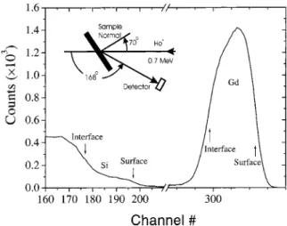
Gd and Si areal densities were determined by Rutherford backscattering spectrometry ~RBS! of 0.7 MeV He1 ions,
detected at a scattering angle of 168° with a sample tilt of 70°. The spectrum of the as-deposited film used for these studies is shown in Fig. 1. The areal density of 16O oxygen was determined by nuclear reaction analysis using 0.85 MeV deuterons to induce the 16O(d, p)17O reaction,7 whereas the areal density of 18O was determined by the 18O( p,a)15N
reaction.11 The narrow resonance of the 18O( p,a)15N
reac-tion at 151 keV (GR5100 eV) was used to profile the 18O
concentration and the narrow resonance of the 29Si( p,g)30P reaction at 414 keV (GR<100 eV) was used to perform
nar-row resonance profiling of 29Si.11
a!
Electronic mail: [email protected]
b!Permanent address: Korea Institute of Geoscience and Mineral Resources,
30 Kajung-dong, Yusung-ku, Taejon, Korea 305-35.
FIG. 1. Gd and Si signals in the RBS spectrum of an as-deposited GdSi1.4O4.3film obtained with 0.7 MeV He1ions using the geometry shown
in the inset.
APPLIED PHYSICS LETTERS VOLUME 79, NUMBER 16 15 OCTOBER 2001
2618 0003-6951/2001/79(16)/2618/3/$18.00
As deposited, the film composition was determined to be GdSi1.4O4.1. After annealing 2 min in vacuum at 800 °C
fol-lowed by 1 min in18O2at 800 °C, the integrated intensity of
the 18O peak increased while the 16O signal remained con-stant so that the composition of the sample was that of a pseudobinary alloy consisting of 27% Gd2O3and 73% SiO2
(GdSi1.4O4.3). During this oxygen annealing there was no
evidence for a change in Si or Gd (1.331015cm22)
concen-tration in the films.
To better quantify the change in O and Si profiles, two sets of samples were prepared, one set annealed for 1 min in
18
O2 at 600, 700, or 800 °C, and the other annealed at the
same temperatures after a 2 min vacuum anneal at 800 °C. A final sample was annealed 2 min in vacuum at 700 °C and 1 min in18O2at 800 °C to determine the sensitivity of oxygen
diffusion to the vacuum annealing temperature. No signifi-cant changes were discernable in the Si and Gd RBS signals after annealing. Typical excitation curves for the
18O( p,a)15
N and 29Si( p,g)30P reactions obtained on the GdSi1.4O4.3 sample are shown in Fig. 2. The 18O excitation
curves in Fig. 2~a! were converted into profiles with subna-nometer depth resolution using the program SPACES.12 The results shown in Fig. 3 indicate that oxygen does diffuse in the films and that the diffusion rate is lower as a result of the densification of the film, if the sample is first annealed in vacuum at 800 °C. Comparing the samples annealed in18O2
at 800 °C after vacuum anneals at 700 or 800 °C demon-strates that the higher-temperature vacuum anneal is more effective in reducing the oxygen diffusion.
The annealing has no effect on the29Si excitation curves of Fig. 2~b!; apparently, silicon does not diffuse in these gadolinium silicate films, during either oxygen or vacuum annealing, at temperatures up to 800 °C. To corroborate this, the samples were examined by x-ray photoelectron spectros-copy using a Mg Ka x-ray source at a low takeoff angle of 30°, where the measurements are surface sensitive or at 65°, in the bulk-sensitive mode. A single Si 2 p line, characteristic of fully oxidized silicon, was observed and its position ~103 eV! and width ~1.69 eV! did not vary with the takeoff angle or annealing over the full range of annealing conditions de-scribed above.
Si readily diffuses into metals such as Y, and subsequent oxidation results in the formation of a silicate layer.13 Vacuum annealing of very oxygen-deficient zirconium sili-cate films ~@Zr#1@Si#5@O#/1.5! on Si resulted in Si–Si pre-cipitates accumulating at the sample surface as a result of silicon diffusion from the substrate.14
Si has also been shown to incorporate during the depo-sition of lanthanum and yttrium oxide films formed by atomic-beam deposition using La or Y and O beams15 or during e-beam deposition of lanthanum oxide from pressed powder targets.16In the latter films, which were initially oxy-gen rich ~@O#.3/2@La#12@Si#!, further Si diffusion was ob-served after annealing at temperatures as low as 750 °C. The diffusion of silicon from the substrate is not universally ob-served in aluminum oxide films10 and may not occur in all zirconium or hafnium silicate films.1More experiments need to be performed to determine the factors determining Si dif-fusion in high-k films, but the apparent tendency of gado-linium silicate films to have a slight oxygen deficiency, rather than a pronounced excess or deficiency, may be a significant advantage.
To determine the effect of annealing at temperatures higher than 800 °C, a 30-nm-thick Gd0.23Si0.14O0.63film was
annealed in O2 for 2 min at 900 °C. The high-resolution
FIG. 2. ~a! Alpha yield of the nuclear reaction 18O( p,a)15N around the resonance at 151 keV. ~b! Gamma yield of the nuclear reaction29Si( p,g)30P
around the resonance at 414 keV. Samples were annealed 2 min in vacuum and/or 1 min in 18O
2; ~jjj! as deposited, ~ddd! 800 °C vacuum,
~mmm! 800 °C vacuum1800 °C18O
2, and ~lll! 800 °C18O2.
FIG. 3. Concentration profiles of18O obtained usingSPACESsimulations of narrow nuclear resonance data: open symbols, preannealing in vacuum at 800 °C for 2 min followed by annealing in18O2for 1 min; cross-centered
symbol, preannealing in vacuum at 700 °C for 2 min followed by annealing in18O2for 1 min; solid symbols, no preannealing in vacuum, annealing in 18O
2 for 1 min; and dashed line, annealing only in vacuum at 800 °C
(expanded310).
2619 Appl. Phys. Lett., Vol. 79, No. 16, 15 October 2001 Landheeret al.
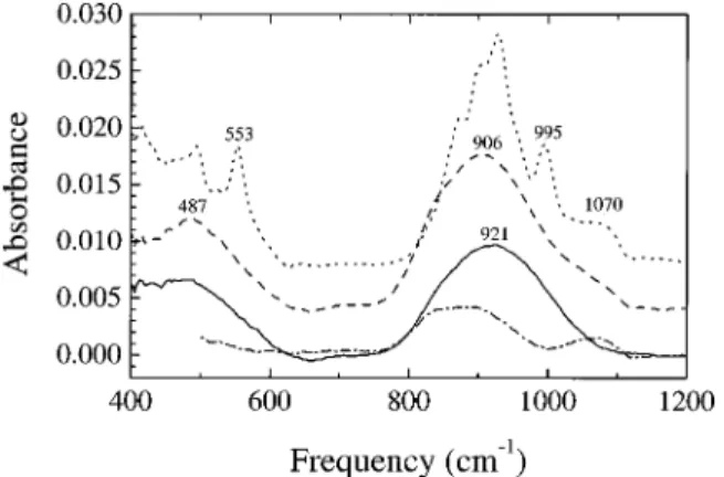
transmission electron microscope photograph of the annealed film has a single distinct 3.5-nm-thick interfacial layer be-tween the Si and the amorphous film. Electron energy-loss spectra of the Gd N4,5 peak were obtained using a Philips
CM20 STEM equipped with a field-emission gun and an energy-loss imaging filter ~Gatan Model 678!. No gado-linium was detected in the interfacial layer. To shed more light on the nature of this layer, Fourier transform infrared spectroscopy was performed on this sample at normal inci-dence. In the spectrum obtained by subtracting the spectrum of the as-deposited film from that of the annealed film, two characteristic peaks centered around 875 and 1068 cm21 were evident, as shown in Fig. 4. Bands at 1070, 900, and 850 cm21 in aluminosilicate,17 or alkali silicate,18 glasses have been attributed to Si–O stretching vibrations of SiO4/2
tetrahedra involving zero, three, or four nonbridging oxy-gens, respectively. Thus, our spectra indicate that significant numbers of the SiO4/2tetrahedra in the interfacial layer have
one or more nonbridging oxygens per tetrahedron.17 High-resolution transmission electron microscopy re-vealed that films annealed in O2at 1000 °C remained
amor-phous but for those annealed for 15 s at 1050 °C the layer above the interfacial layer had crystallized. In Fig. 4 the spectrum of the film annealed at 1050 °C showed further peaks characteristic of a crystalline film. If 15 s anneals at 1050 °C are required to anneal implants using conventional device processing sequences, the anneals would have to be done in an oxygen-free environment on films with a higher
silicon dioxide fraction than those studied here, but more work needs to be done to study the effect of these anneals on the electrical properties of the interface.
In conclusion, it has been shown that gadolinium silicate films deposited by e-beam evaporation are not susceptible to Si diffusion during either vacuum or oxygen annealing. Oxy-gen diffuses through the films, eliminating any oxyOxy-gen defi-ciency and resulting in pseudobinary alloys of Gd2O3 and
SiO2. Subsequently, extra oxygen can diffuse through the
films to the oxide/Si interface, allowing some flexibility in engineering the electrical properties of the interface.
The authors wish to thank T. Quance, E. Estwick, and J. P. Philips for their technical support. J.M., I.J.R.B., R.P.P., and L.M. are grateful for financial support from CNPq and FAPERGS ~Brazil!.
1G. D. Wilk, R. M. Wallace, and J. M. Anthony, J. Appl. Phys. 89, 5243
~2001!.
2K. J. Hubbard and D. G. Schlom, J. Mater. Res. 11, 2757 ~1996!. 3G. D. Wilk and R. M. Wallace, Appl. Phys. Lett. 76, 112 ~2000!; J. Appl.
Phys. 87, 484 ~2000!.
4W. J. Qi, R. Nieh, E. Dharmarajan, B. H. Lee, Y. Jeon, L. Kang, K. Onishi,
and J. C. Lee, Appl. Phys. Lett. 77, 1704 ~2000!.
5J. Kwo, M. Hong, A. R. Kortan, K. T. Queeney, Y. J. Chabal, J. P.
Man-naerts, T. Boone, J. J. Krajewski, A. M. Sergent, and J. M. Rosamilia, Appl. Phys. Lett. 77, 130 ~2000!.
6
D. Landheer, J. A. Gupta, G. I. Sproule, J. P. McCaffrey, M. J. Graham, K.-C. Yang, Z.-H. Lu, and W. N. Lennard, J. Electrochem. Soc. 148, G29 ~2001!.
7J. A. Gupta, D. Landheer, G. I. Sproule, J. P. McCaffrey, M. J. Graham,
K.-C. Yang, Z.-H. Lu, and W. N. Lennard, Appl. Surf. Sci. 173, 318 ~2001!.
8J. A. Gupta, D. Landheer, J. P. McCaffrey, and G. I. Sproule, Appl. Phys.
Lett. 78, 1718 ~2001!.
9A. I. Kingon ~unpublished!; see, also, A. I. Kingon, J.-P. Maria, and S. K.
Streiffer, Nature ~London! 406, 1032 ~2000!.
10
C. Krug, E. B. O. da Rosa, R. M. C. de Almeida, J. Morais, I. J. R. Baumvol, T. D. M. Salgado, and F. C. Stedile, Phys. Rev. Lett. 85, 4120 ~2000!; M. Copel, ibid. 86, 4713 ~2001!.
11I. J. R. Baumvol, Surf. Sci. Rep. 36, 1 ~1999!. 12
I. Vickridge and G. Amsel, Nucl. Instrum. Methods Phys. Res. B 45, 6 ~1990!.
13J. J. Chambers and G. N. Parsons, Appl. Phys. Lett. 77, 2385 ~2000!. 14J. Morais, E. B. O. da Rosa, L. Miotti, R. P. Pezzi, I. J. R. Baumvol, A. L.
P. Rotondaro, M. J. Bevan, and L. Colombo, Appl. Phys. Lett. 78, 2446 ~2001!.
15S. Guha, E. Cartier, M. A. Gribeliuk, N. A. Bojarczuk, and M. C. Copel,
Appl. Phys. Lett. 77, 2710 ~2000!.
16M. Copel, E. Cartier, and F. M. Ross, Appl. Phys. Lett. 78, 1607 ~2001!. 17
D. J. T. Kohli, R. A. Condrate, Sr., and J. E. Shelby, Phys. Chem. Glasses
34, 81 ~1992!.
18A. J. G. Ellison and P. C. Hess, J. Non-Cryst. Solids 127, 247 ~1991!. FIG. 4. Fourier transform infrared spectra of the 30-nm-thick
Gd0.23Si0.14O0.63sample: ~ ! as deposited; ~----! after annealing at 900 °C
in O2for 120 s; ~¯••! after crystallization at 1050 °C in O2for 15 s; and
~ • • • ! difference, first two spectra.
2620 Appl. Phys. Lett., Vol. 79, No. 16, 15 October 2001 Landheeret al.