HAL Id: hal-03017738
https://hal-cnrs.archives-ouvertes.fr/hal-03017738
Submitted on 30 Nov 2020
HAL is a multi-disciplinary open access
archive for the deposit and dissemination of
sci-entific research documents, whether they are
pub-lished or not. The documents may come from
teaching and research institutions in France or
abroad, or from public or private research centers.
L’archive ouverte pluridisciplinaire HAL, est
destinée au dépôt et à la diffusion de documents
scientifiques de niveau recherche, publiés ou non,
émanant des établissements d’enseignement et de
recherche français ou étrangers, des laboratoires
publics ou privés.
Spectroscopic Ellipsometry Imaging for Process
Deviation Detection via Machine Learning Approach
Thomas Alcaire, Delphine Le Cunff, Victor Gredy, Jean-Herve Tortai
To cite this version:
Thomas Alcaire, Delphine Le Cunff, Victor Gredy, Jean-Herve Tortai. Spectroscopic Ellipsometry
Imaging for Process Deviation Detection via Machine Learning Approach. 2020 31st Annual SEMI
Advanced Semiconductor Manufacturing Conference (ASMC), Aug 2020, Saratoga Springs, United
States. pp.1-6, �10.1109/ASMC49169.2020.9185349�. �hal-03017738�
XXX-X-XXXX-XXXX-X/XX/$XX.00 ©20XX IEEE
Spectroscopic Ellipsometry Imaging for Process
Deviation Detection via Machine Learning Approach
Thomas Alcaire STMicroelectronics Crolles, France [email protected] Delphine Le Cunff STMicroelectronics Crolles, France [email protected] Victor Gredy STMicroelectronics Crolles, France [email protected] Jean-Hervé Tortai
Univ. Grenoble Alpe, CNRS, CEA-LETI Minatec, LTM
Grenoble, France [email protected]
Abstract—Spectroscopic ellipsometry is a very sensitive
metrology technique to accurately measure the thickness and the refractive index of the different layers present on specific dedicated metrology targets. In parallel, optical defectivity techniques are widely implemented in production lines to inspect a large number of dies and catch physical and patterning defects during the process flow. It becomes then of interest to explore a new approach overlapping metrology and defectivity by using the sensitivity of metrology tools on a full wafer scale. In our case, spectroscopic ellipsometry’s optical response was collected directly on the dies to capture specific deviations such as film properties and thickness variation. This is an innovative strategy that requires a model-less approach, combining an automatic ellipsometry mapping generation and a smart classification via a machine learning algorithm. In this paper, we will present such approach on two industrial use cases and explain how an image classification algorithm can be implemented to automatically detect the process drift on the latter.
Keywords— Spectroscopic ellipsometry, model-less, process control, machine learning
I. INTRODUCTION
In the standard approach, Spectroscopic Ellipsometry (SE) is used to measure the thicknesses and the optical indices of multistack layers deposited on a substrate. Since many years now, spectroscopic ellipsometry is also routinely used for Optical Critical Dimension (OCD) control through modeling of periodical patterned structures. Both applications require a perfect knowledge of the layers and/or of the structure constituting the metrology targets in order to develop a realistic mathematical model. By simulating the spectroscopic ellipsometry response and after a reverse problem-solving operation, one can then extract the parameters of interest (thickness, n and k, CD, Side Wall Angle…). This process can be very time consuming and request heavy engineering effort (pre-characterization, cross comparative…). Both approaches also require the design of specific blanket or periodical targets on sacrificial area of the product wafer.
In recent years, in order to accelerate the learning curve of new technological developments, model-less strategy have been introduced in the metrology field. In this context, one will rely on the strength of machine learning for data treatment rather than on an accurate underlying model. Machine Learning is a subset of artificial intelligence which enables computer systems to learn from data without being explicitly programmed. This new alternative for data treatment has already been explored for semi-conductor process control in several previous studies such
as for example: predictive metrology [1][2] or detection of voids in copper lines [3].
In this paper, we explored the benefit of spectroscopic ellipsometry mapping measurement as well as data treatment for full wafer process control. Due to the complexity of the optical response from the underlying design structure of the product wafer, we implemented a model less approach to detect local process deviation. Two use cases of process anomalies are reported in this paper: full wafer area or full chip area inhomogeneity. For the latter, the SE raw data can be processed through machine learning to automate the deviation detection protocol.
II. EXPERIMENTAL SETUP AND PROTOCOL
In this section, we describe the spectroscopic ellipsometer equipments that were used for this study as well as the protocol for SE mapping acquisition and image generation.
A. Spectroscopic ellipsometers
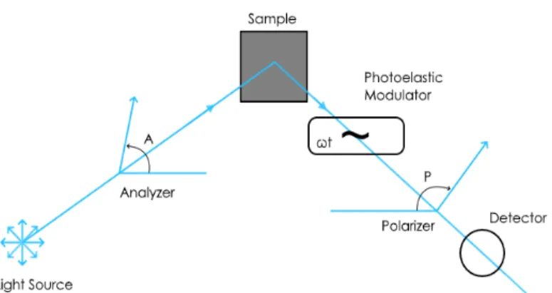
Fig. 1 - Schematic of the phase-modulated ellipsometer working principle.
Industrial SE metrology equipments are completely inappropriate for scanning a full wafer surface due to their small spot size. We then used two laboratory equipments with a larger footprint on the surface of the wafer. The two systems are phase-modulated ellipsometers supplied by HORIBA. Due to the high modulation frequency of the phase (50 kHz), both ellipsometers allow fast measurements of ellipsometry angles at a single wavelength (< 200 ms per point). It means that if one wavelength is chosen, the full wafer scanning by ellipsometry will be sufficiently fast.
A basic schematic of the phase-modulated ellipsometer principle is presented in Fig. 1 and the exact configuration can be found in [2]. For phase-modulated ellipsometer, the raw data gathered are the ellipsometry parameters Is and Ic, which values are then bound between -1 and 1. These are linked to the usual ellipsometric angles Δ and Ψ through equations (1) and (2).
2 (1) 2 (2) The first equipment is an UVISEL 1 designed for 200mm wafers and is therefore limited to acquisitions up to 100mm radius with an incident angles that can vary from 55° to 85°. The measuring spot size is of 0.14x0.08mm. The light source wavelength covers 190 to 850nm. It is then well suitable for localized mapping of specific region of interest. The second is an inline UVISEL 2 (IMPACT platform), which covers a large broadband spectrum (150nm - 2µm), which is able to collect responses at any coordinates on the surface of a 300mm wafer, with a fixed incident angle of 70°. This equipment was then used for 300mm full wafer scanning considering its large measuring spot size of 8x5mm.
B. Acquisition Protocol and Image generation
A specific protocol was implemented for data acquisition which is summarized in Fig. 2. As a preliminary step to ellipsometry mapping acquisition, a routine is performed to select the optimum angle and wavelenght to get maximum sensitivity.
Fig.2 – Overview of the ellipsometry imaging protocol.
1) Angle of incidence selection
For the case of UVISEL 1 equipment, for which the angle of incidence can be varied with a goniometer, we performed spectroscopic scans of the region of interest at different angles
in order to select the optimum angle providing the largest variation in amplitude for Is or Ic (Fig.3).
Indeed, ellipsometers measure the ratio of the amplitude reflection coefficients (rp/rs). Those coefficients strongly
depend on the angle of incidence. At Brewster angle, the difference between the parallel coefficient (rp) and the
perpendicular coefficient (rs) is maximal, and the sensitivity for
the measurement is optimal. Thus, this condition could correspond to an optimal configuration for our acquisition. Unfortunately, considering the complexity of the dies, the Brewster angle can hardly be theoretically modeled, and we have to rely on experimental testing for the optimized incidence angle selection.
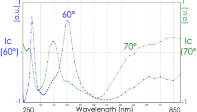
Fig 3 – Example of Ic variable angle spectroscopic response and optimal angle of incidence selection, which is 60° here.
2) Wavelength selection
In order to get the maximal sensitivity to any changes in optical responses, a spectroscopic scan was performed in the area of interest/a typical die at the optimal angle previously chosen. The obtained spectrum allows us to choose the single wavelength that will be used to rapidly perform the Is and Ic acquisition. This wavelength is set by finding the intercepts of the Is and Ic curves of the spectroscopic scan. Among those intercepts’ positions, the one that presents the maximal local slope and the maximum gain for the detector signal is chosen. Any slight variations in the material properties will then result in large variations of the ellipsometry signal on both Is and Ic components (Fig. 4). The purpose of selecting a single wavelength is to drastically reduce the acquisition time. Indeed, a single wavelength acquisition takes a couple of seconds per point to be performed, when a full spectroscopic scan would take minutes per point. Considering that we used mapping grids composed of thousands of points, a spectroscopic acquisition is therefore unrealistic. By choosing a single wavelength, we preserve the sensitivity of spectroscopic ellipsometry, while keeping acquisition times reasonable.
Fig. 4 – Example of Is and Ic spectroscopic response at the optimal angle and optimal wavelength selection, which is 410nm here.
3) Image generation
The selected conditions for wavelength and potentially angle are then applied for ellipsometric (Is and Ic) acquisitions on a dense mapping grid of the area of interest. This was implemented using a custom-written Python script. The ellipsometry images are then generated by assigning each value of Is and Ic to their corresponding coordinate, and in turn obtain two ellipsometry mappings of the region of interest. The final cartographies are obtained after performing a cubic interpolation between the measured points. Examples of Ic and Is cartographies can be found in Fig. 8.
III. RESULTS
This section describes the results obtained conducting this acquisition protocol on two use cases of process variation: respectively “Intrawafer nitride passivation layers properties
variation” and “Color resist layers intradie thickness variation”.
A. Intrawafer nitride passivation layers properties variation
For the first use case, we tested the sensitivity of model-less ellipsometry approach to detect intra wafer signature resulting from difference in stress of nitride layers [3] (both on blanket and on patterned wafer). These nitride layers used for the study are dielectric films acting as isolation between metallic Al contact pads of patterned wafer. For some cases, changes in mechanical properties can lead to yield issues (Fig. 5a). The analysis was then performed on the full wafer surface. The mapping grid used and presented in Fig. 5b is composed of 6000 measurement points evenly spread on the 300mm wafer surface. Is and Ic acquisitions were performed with UVISEL 2 equipment. A duration of 3.5 hours was necessary for each full wafer acquisition.
Fig.5 – a) Yield wafer map showing a diametrical intra-wafer signature and b) dense mapping grid defined for 300 mm wafer surface scanning.
1) Blanket wafer analysis
Blanket nitride layers on silicon can easily be characterized by industrial in-line ellipsometry as already demonstrated in [5]. For this specific use case, a strong inhomogeneity was observed linked to changes in the refractive index of the layer (Fig. 6). As a first test, we tested our model-less spectroscopic ellipsometry approach to characterize the same wafer.
Fig.6 – In-line spectroscopic ellipsometry measurement map on the blanket wafer for refractive index (37 points).
Following the protocol described in Fig.2, a spectroscopic scan was performed to select the optimal wavelength for the further analysis. As it can be seen in Fig.7, multiple wavelengths were eligible but in order to maximize luminous intensity from our source, a 500nm wavelength was retained.
Fig.7 – Ic and Is spectroscopic scan on the blanket wafer for the optimal wavelength selection.
The Is and Ic response collected on UVISEL 2 using the mapping presented in Fig. 5b are presented in Fig. 8. The intra wafer signature cartographies obtained through model less spectroscopic ellipsometry is extremely similar to the one
obtained with the in-line measurements except that they benefit from a larger amount of data. This proves the sensitivity of this approach to detect variation in the deposited film properties, without the need to develop a theoretical model of the stack.
Fig.8 – Model-less spectroscopic ellipsometry cartographies (6000 points) of the shifted blanket wafer.
2) Product wafer analysis
By opposition to blanket wafers, product wafers are composed of an intricate and complex stack of layers, for which an accurate model would be very arduous to produce. This, combined with the lack of metrology target structures available for some cases at the extreme edge, would make this kind of intrawafer variation hardly detectable by classical spectroscopic ellipsometry measurements.
As for blanket layers, the protocol starts with a spectroscopic scan (Fig. 9) to select the wavelength to be used for the further full wafer acquisition.
Fig.9 – Is and Ic spectroscopic scan on the patterned wafer for the optimal wavelength selection, which is 338 nm here.
The wavelength was set to 338nm to gather the raw ellipsometric data, and the resulting cartographies are displayed in Fig. 10a, where a clear intrawafer signature is observed, compatible with the one observed on the blanket wafer. The results were compared to the characterization results obtained with a full wafer interferometry technique (PWG system from KLA) which measures notably local stress and nano-topography. The PWG stress cartography is shown in Fig. 10b and displays an extremely similar signature with respect to the model-less ellipsometry ones.
Fig.10 – a) Model-less spectroscopy ellipsometry cartographies (6000 points) and b) PWG stress cartography of a patterned wafer.
In conclusion, we proved the sensitivity of our model-less approach to detect changes in material properties at the wafer scale, first on a blanket wafer, but more interestingly, on a product wafer.
B. Color resist layers intra die thickness variation
For the second use case presented here, our intent was to detect intra wafer thickness variation induced by color resist deposition. The color resists are used as optical filters to perform RGB (Red, Green, Blue) pixel arrays for imagers devices. Due to complex topography effect on product wafers, the spin-coating deposition can lead to inhomogeneity in the resist thickness causing a radial striations signature. As we can see on the optical inspection image (Fig. 11a), those striations are more pronounced at the edge of the wafer than at its center. Consequently, we focused the study on dies at the edge of the wafer, and the acquisition grid was set up as illustrated in Fig. 11b. We measured 5 dies (1500 points in each die of 48mm²) for each acquisition, one at center as a reference, and 4 on the edge of the wafer.
Fig.11 – a) Optical inspection showing the presence of striations on the edge of the wafer, and their absence in the center and b) schematic of the mapping grid used for multiple die ellipsometry imaging.
For such use case, where a full wafer acquisition is not required, we could use the UVISEL 1 and benefit from the angle optimization step presented earlier (in II.B.). We observed an enhanced sensitivity for a 55° angle of incidence (Fig. 12). It is supposed that this angle corresponds to the effective Brewster angle of the material studied (optical refractive indices in the 1.6 range), which explains the increased ellipsometric response.
Fig.12 – Spectroscopic scan (only Is is displayed for visibility) done at 55° and 70° showing a stronger ellipsometric response for the smaller angle of incidence.
For this incident angle, the optimal wavelength was determined to be 315 nm (Fig. 13). This wavelength selection is even more critical here considering the relatively small amplitude variation observed in the collected spectrum.
Fig.13 – Spectroscopic scan done at an angle of incidence of 55° for the optimal wavelength selection.
Following the acquisition protocol, we performed the multiple dies acquisitions and the cartographies obtained are show in Fig. 14. The model-less spectroscopic ellipsometry results were compared to PWG nanotopography mappings. We observe that no striations are detected at the center of the wafer both on PWG and ellipsometry cartographies. On the contrary, the 4 other dies exhibit striations that both PWG and ellipsometry could detect.
In conclusion of this use case, we were then able to detect this process deviation related to variation in thickness with a model-less spectroscopic ellipsometry approach on a product wafer, in the same way as the PWG technique. It is to be noted that PWG is limited to topography below 150nm and subsequently can suffer from reconstruction errors.
Fig.14 – Comparison between PWG nanotopography and model-less spectroscopic ellipsometry cartographies (1500 points) on the same die at the center and edge of wafer.
IV. MACHINE LEARNING TREATMENT
To go further in the data treatment of the ellipsometry images acquired for color resist as detailed in Section III.B, we investigate the implementation of a machine learning algorithm to automate the striation detection. We set up an artificial intelligence algorithm capable of classifying images in two categories: Striated and Flawless dies.
First of all, a specific pre-treatment of the images is needed for a machine learning algorithm to work properly. The pre-treatment extracts important features from the images and was performed using descriptors which are image processing tools each one being specific to the detection of one feature (e.g. line or edge detection). Their output is often a vector composed of numerical values, which can now be treated by a supervised learning algorithm. Those features are selected so that they allow the algorithm to effectively distinguish a class from another. Because the discriminatory feature in this use case is the presence of striations, we chose the canny edge detector [6] as descriptor. By definition, supervised learnings training data is required to be labeled with its corresponding class in order for the algorithm to learn. Once trained, it is able to automatically classify new cartographies, and even to use them as further training. A wide variety of supervised learning algorithms are available, but Logistic Regression gave us the best results.
As it can be seen in SE images of Fig.14, the effects at the edge of the die could greatly influence the efficiency of the prediction algorithm. To avoid this potential issue, only the center of the die was then kept for this part (Fig. 15a). Also, being limited by the amount of experimental data at our disposal, we used synthetic mappings. They are generated to mimic the experimental ones, in order to have sufficient data to properly train the machine learning algorithm. Our dataset was then composed of a training set of 200 synthetic mappings (100 striated and 100 flawless) and a test set of 50 experimental mappings (40 striated and 10 flawless). An example of each cartography is shown in Fig. 15b. The synthetic cartographies features are then extracted by the descriptor and are used to train the machine learning algorithm. The machine learning
predictive efficiency is finally tested on the experimental cartographies.
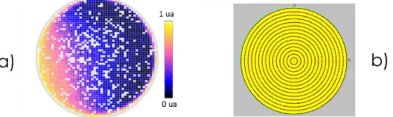
Fig.15 – a) Reduced region studied to remove uncertainty due to the positioning and b) examples of each of the cartographies used during the machine learning treatment: Flawless and Striated cartographies obtained through model-less spectroscopy ellipsometry, and Flawless and Striated cartographies generated artificially.
For this first test of implementation, we actually obtained a very good prediction accuracy of 96 % (48/50) on our experimental ellipsometry mappings. A visualization of the dies identified (striated or flawless) by machine learning is shown in Fig. 16. Our model-less spectroscopic ellipsometry approach combined with a machine learning algorithm is then able to successfully automatically detects this process deviation.
Fig.16 – Visualization of the prediction from the machine learning algorithm on the experimental ellipsometry cartographies
V. CONCLUSION
In this paper, we showed that a model-less strategy based on ellipsometry raw signal treatment is capable of detecting process deviations on full product wafer surface or on full dice of product wafer. Besides, the coupling of this technique with a machine learning algorithm, built as an image classifier, can allow an automatic detection of process deviation with a very high accuracy. Such combined approach can be applied to other sources of optical techniques more traditionally used for wafer physical defect inspection.
ACKNOWLEDGMENTS
This work has received funding from the Electronic Component Systems for European Leadership Joint Undertaking under grant agreement No 826589 (project MADEin4). This Joint Undertaking receives support from the European Union Horizon 2020 research and innovation program and, Austria, Belgium, France, Germany, Hungary, Ireland, Italy, Netherlands, Romania, Sweden.
This work has also been supported by the French ANR program Investissements d’Avenir EQUIPEX, contract number ANR-10-EQPX-33
REFERENCES
[1] P. Timoney et al., "Implementation of machine learning for high-volume manufacturing metrology challenges (Conference Presentation)", Metrology, Inspection, and Process Control for Microlithography XXXII, 2018.J. Clerk Maxwell, A Treatise on Electricity and Magnetism, 3rd ed., vol. 2. Oxford: Clarendon, 1892, pp.68–73.
[2] J. Gaudiello et al., "Electrical test prediction using hybrid metrology and machine learning", Metrology, Inspection, and Process Control for Microlithography XXXI, 2017.K. Elissa, “Title of paper if known,” unpublished.
[3] D. Kong et al., "Machine learning and hybrid metrology using scatterometry and LE-XRF to detect voids in copper lines", Metrology, Inspection, and Process Control for Microlithography XXXIII, 2019. [4] O. Acher, E. Bigan and B. Drévillon, "Improvements of phase ‐
modulated ellipsometry", Review of Scientific Instruments, vol. 60, no. 1, pp. 65-77, 1989.
[5] V. Brouzet et al., "Full Wafer Stress Metrology for Dielectric Film Characterization: Use Case", 2019 30th Annual SEMI Advanced Semiconductor Manufacturing Conference (ASMC), 2019.
[6] J. Canny, "A Computational Approach to Edge Detection", IEEE Transactions on Pattern Analysis and Machine Intelligence, Vol. PAMI-8, No. 6, pp. 679-69PAMI-8, 1986.