A BINARY QUANTIZER
itITH A RESOLUTION OF ONE PART IN A THOUSAND
by
JULIAN E.
GROSS
B.S,. Masusachusetts Institute of Technology 1951
SUBMITTED
IN PARTIAL FULFILLMEWT
OF THE
E~QUIREM~VTS
FOR THE
DEGREE
OF
MASTER OF SCIENCEat the
MASSACHUSETTS INSTITUTE OF TECHNOLOGY
(1951)
Signature of Author
Certified by
..
u
ofv lev-.-. 0 0 . 0. 1 18*5a....1... ... a.*. of Elect, Eng. May 18, 1951
'I,
....
.... ...
imans, Dept. Committee an
uate Students v
6• 4 6 p +"p~`·r i ab Y·? B 5.
6
INST. AUG 6 1951)ABSTRACT
A BINARY QUATTIZER WITH A RESOLUTION OF
ONE PART IN A THOUSAND by
JULIAN E. GROSS
Submitted for the degree of Master of Science in the Department of Electrical Engineering May 18, 1951.
A logical design for a binary quantizer with a resolution of one part in one thousand and a sempling rate of one thousand times per second has been developed. The proposed system is all electronic and may be classified as a 2n/2+1 -step device as contrasted with the more commno n-step and 2n-step quantizers.
The design developed employs a voltage comparator to transform the voltage to be coded into a time interval. A certain number of fixed time intervals are subtracted from the main interval and the remainder
is essentially multiplied by 32. The intervals subtracted and the multi-plied remainder are used to activate gate circuits which gate pulses
into a binary counter.
In evolving the design for a circuit to meet the specifications chosen, emphasis was placed on the development of those parts of the
circuit which had not been sufficiently developed for application to this problem. In particular, development ~ork has been carried out on a voltage comparator to definitely establish that a resolution of one
part in a thousand is possible. Also, a circuit has been designed to transform a variable time interval of 9-12 microseconds into a gate pulse width 32 times as long to an accuracy sufficient for use in"i the proposed
system of quantization.,
-ii-ACKNOWLEDGEMENT
The author wishes to express his sincere appreciation for the invaluable aid and encouragement rendered by Professor T.F. Jones during the course of this research.
TABLE OF CONTENTS
Section Page
Abstract ... ... ... ... .... ... ... ... ii I* Introduction ...4...•....•.•..•.•. ...
1.0 Objective
1.1 Theory of quantization and Background
11, The Proposed System ... ... .
2.0 Theory of Operation 2.1 The Block Diagram 2.2 Circuit Requirements III. The Comparator
53.0 Specifications
3.1 Experimental Results 3,2 Circuit Operation 3.3 Circuit Components
3.4 Validity of Method of Measurementl
3.5 Analysis and Discussion of Errors 3.6 Summary and Conclusions
IV. The Time Amplifier ... 4.0 Specifications
4.1 Experimental Results
4.2 The Block Diagram
4.3 Theory of the Multiplier 4.4 The Schematic Diagram
4.5 Measurements on the Time Amplifier
4,6 Summary Discussion of the Time Amplifier
V. Conclusions ... ...
5.0 Summary
5.1 Suggestions for Further Study
Appendixes ... ... ... ... Bibliography ... . 1
1
15
5 6 8 15 1s 15 1718
19
28
30
30
30
33
36
38
44
45 47 4748
50
-1-i
Seetion I
Introduction
1.0 Objectives:
The object of this thesis has been to evolve a logical design for
a devise to quantise eontinuously varying information available as a voltage into a binary code representing the instantaneous amplitude at equally spaced intervals of time. The sampling rate was chosen to be a thousand times per second and the resolution to be sought was set at one part in a thousand. These specifications represent a reasonable extrapolation of present achievements in the field.
In evolving the design of a circuit to meet these specifications emphasis has been plaoed on the development of those parts of the oirouit -which had not been sufficiently developed for application to this problem. In particular, development work was carried out on a. voltage cgaparator to definitely establish that a resolution of one part in a thousand is possible. Also, a circuit has been designed
to transform a variable interval of time of 0-12 mioroseconds into a gate pulse width 32 times as long to -an accuracy sufficient for use in the quantiser.
1.1 Theory of Qfantization and Backgrounds
In general, functions representing physical quantities such as temperature, pressure, velocity, etc., are continuously variable and
-2-may be represented by an analagously varying electrical quantity. It is often desirable to operate upon such analogue quantities using digital techniques which require that the data be expressed in some code representing uniquely its amplitude at certain discrete intervals of time. Most commonly the code is a binary number and the intervals between samples are equal. It is generally desirable to sample and code as frequently as possible and to have a large number of codes so that the quantized steps are small. This gives the most aeourate numerical representation of the continuous function. The accuracy or
resolution of coding is seen to be the reciprocal of the highest num-ber of unique codes possible.
For a maximum binary count of 2n, n binary digits are used. It
follows that ten binary digits are necessary to obtain a maximum of
1000 unique codes as is desired here.
There are several methods of quantization used in current practice. Perhaps the simplest is straightforward counting in the time domain.. A voltage directly proportional to the insantaneous count is compared to the voltage representing the function to be coded. The number of counts completed by the time of coincidence is a measure of the value of the function at the time of coincidence. This is the so-called "2n-step" type of coding since a maximum of 2n counts may be required in one sampling period. The associated digit register in which the binary number is developed will be subjected to a maximum of 2n
changes of state in the 2n-step coder. Since the frequency of count-ing is limited, the frequency of sampling is limited. Resolution depends upon the accuracy of the coincidence detector.
Systems classified as n-step have been built with an accuracy of one part in S2 at MIT.1* This type of device builds up a reference voltage by means of an n digit binary register in n steps. The ref-erence voltage is compared with the function to be coded at each step and the polarity of the difference determines the succeeding step so as to get a better approximation to the function. This method in-volves decoding the binary number at each step for comparison. Its accuracy is dependent upon the accuracy of both decoding and compar-isorn.
An n-step device to code in what may be termed the space domain has been developed by the Bell Telephone Laboratories, 2 This system
employs a complicated and expensive circuit employing a special cathode ray tube to code to one part in 128. The resolution here depends upon the spacial resolution of the cross section of an electron beam at the
face of the cathode ray tube.
Bibliographic research has revealed no published claims for an accuracy of greater than one part in 256 for a purely electronic
system. An electro-mechanical system having a resolution of one part in 512 has been developed by the Signal Corps of the U.S. Army at the Fort Monmouth Laboratory. This system employs a positional servo-mechanism in its operation and so is limited to only a few independent
samples per second.
At the sampling rate desired, 1000 times per second, only purely electronic methods appear to be feasible. The number of "steps",
* Numerical superscripts refer to numbered references in the bibliography,
inherent in the operation of any particular coding device is of impor-tance because each step requires one or more switching actions in the
electronic circuit. The switching transient limits the frequency of switching in any physically realizable circuit. It would appear that this limits the sampling rate of the 2n-step coder much more than it does the sampling rate of the n-step coder, but consideration must be taken of the fact that each step in the case of the n-step device involves many switching actions vhereas few are required for each step in the case of the 2n-step deviee. If an n-step system were designed employing as many as 10 binary digits, however, it would in all prob-ability have a higher sanpling rate.
The 2n-step coder uses simpler, more completely developed oircuits than current n-step devices. Its accuracy depends principally upon the sensitivity and stability of the voltage comparison device used. The n-step coder requires both comparison and decoder circuits with equally high resolutions. The proposed system may be classified as a 2n/24 1 -step coder. Its accuracy depends upon the resolution of a voltage comparator as in the ease of 2n-step coder to which it bears a close kinship. For the same resolution, however, it is expected that the sampling rate of the proposed system will be greater.
How the two systems will ultimately compare depends upon develop-ment in the field of high speed counters in the case of the 2n-step
coder and upon development of precisely gated sweep generators in the case of the 2n/2+1 -step coder proposed. For the present, both
systems are limited by the capabilities of present day voltage comparators.
Section II
The Proposed System
2.0 Theory_ of oeration:
Basically, the voltage to be coded is converted into a time inter-val proportional to the instantaneous voltage amplitude to an accuracy of better than one part in a thousand. Pulses are generated at such a rate that exactly 32 pulses represent the maximum value of the function. These pulses are gated by the aforementioned time interval and applied to a binary count register of five binary digits which stores the so-called "coarse count". The time interval between the last coarse count gated and the end of the gating interval is effectively multiplied by
32 and used to gate succeeding pulses from the same source. This
so-called "fine count" is applied to another part of the binary register and held. If now the coarse count is multiplied by 32 and added to the fine count it is seen that the function has been quantized into 1024 parts sinoeeeach of the 32. coarse intervals has been broken up into 32 equal parts.
In the work described here the interval between the end of the coarse gating interval and the next succeeding coarse count, pulse is multiplied in duration and used to gate a fine count. This count is then subtracted from 32 in effect to give the true fine count. This
pulse and then taking the 32's complement of the result. To illustrate this, suppose the end of the coarse gating interval occurred 15/52 of the distanoe between two coarse count pulses. Then 17 fine pulses
would be gated and one of these subtracted leaving 16 which is repro-sented by the binary number 10000. The 32's complement of this binary number is 01111 vhieh represents 15, the actual fine count desired. The process of subtracting 1 is actually earried out in the time
multiplier and the complement is automatically taken in the binary count register by the simple expedient of taking the count out of the regis-ter from the appropriate plate circuits of the flip-flops.
It the coarse count binary register is arranged so that it comprises the five highest binary digits of a ten digit register with the fine count register comprising the five lower digits, the coarse count is automatically multiplied by 32 and the entire count appears in the ten digit register taken as a whole.
2.1 The Block Diagram
The process can be made more clear by considering the block dia-gram step by step in conjunction with typical waveforms (Fig. 1.). The Clock Pulse Generator supplies both a master timing pulse every 996 microseconds and the coarse and fine count pulses every 12 micro-seconds. The master timing pulse starts the Main Sweep Generator and turns on the Coarse Count Gate which allows 12 microsecond pulses to
enter the Course Count Register. The Main Sweep Generator generates a sweep which rises 102.4 volts in 32 coarse counts or 384
1111 1 1 II1 1ff I tlII il ii fil ii fi I I I
MASTER TIMING PULSE 12 MICROSECOND PULSES
MAIN SWEEP
COMPARATOR PULSE
Ill1111111111111i COARSE COUNT
FINE COUNT GATE PULSE
111111111 1111 FINE COUNT
Fig. 1. QUANTIZER BLOCK DIAGRAM
"f8*
with the funetion to be coded which is adjusted to have a maximum range
of 102•.4 velts. At the time of equality (within 0.1 volt)• the Comparator
delivers a pulse which turns off the Coarse Count Gate stopping the feed of 12 microsecond pulses into the Coarse Count Register. This
pulse also activates the Time Amplifier which measures the time interval
from then until the next lZ microsecond pulse. The Time Amplifier multiplies this time by 32 and subtracts 12 microseconds, delivering a
gating pulse to the Fine Count Gate which ga-es 12 microsecond pulses into the Fine Count Register. It also feeds a read-out and reset signal to the Count Register at the end of the Fine Count Gate pulse.
It ,an be seen that the maximum number of counts used l 13 be 64,
taking 768 mieroseconds of the sampling interval and leaving 228 micro-seconds recovery time as a minimum.
22I Circuit Requiremnents
We may now take each block individually, considering the operations it is to perform and the restrictions of stability and precision that must be imposed upon it if the quantizer as a whole is to meet the
specifications of resolution and sampling time previously decided upon.,
i. Clock Pulse Generator.
It is extremely important that the Cloek Pulse Generator deliver pulses that do not vary in time with respect to each
other by more than about .05 microseconds. The interval between pulses does not necessarily have to be an accurate 12. microseconds as long as the rest of the oireuit is cali-brated for the actual interval. The master timing pulse
.9-must occur coincident with one of the 12 microsecond pulses, and must recur at some multiple of 12: microseconds such that
the master timing pulses will be spaced approximately 1000 microseconds apart. The pulses must have a rise time of the order of .05 microseconds and a duration not to exceed 0.3 microseconds. The master timing pulse may have a longer duration but the rise time must be the same as for the 12 microsecond pulses.
These requirements are fairly easily met with present
day pulse generating equipment using a crystal oscillator as
a timing mechanism.3 For this reason it is not deemed nee-essary to concentrate effort in this direction.
ii. Main Sweep Generator.
The Main Sweep Generator must deliver a sawtooth which is linear to better than 0.1% of full scale and which is triggered on with a delay of less than 0.5 microseconds in starting. Furthermore, the starting voltage may not drift as much as 0.1% of maximum sweep voltage with respect to the zero reference of the input function. The full scale sweep has been arbitrarily set at 102.4 volts for this application.
A great deal of development has been applied to sweep and integrator circuits and a high state of perfection has been achieved. 4 It is possible to use circuits commercially available for this component of the quantizer.
iii. Comparator:
4*10-voltage with amplitude 102.4 volts applied for comparison with a relatively fixed input signal. For the time being we
shall consider the input signal held at a fixed voltage for a sampling interval so that it may be considered a constant.
The comparator must indicate the instant of coincidence to within a fine count interval which is .S75 microseconds. Alternatively, it must recognise equality of the voltages applied to better than 0.1 volt. Any fixed "delays"' in
either voltage or time may be calibrated out and the output pulse need not have stringent requirements for rise time or duration,
Many comparison circuits of various types have been designed, but bibliographic research reveales none which meets the exacting requirements listed above. For this
reason a large part of the development y rk done in this thesis has been concerned with the design, test, and analysis
of a voltage oomparator. This is fully covered in section III whieh is devoted to the Comparator.
iv. Time Amplifier:
The Time Amplifier circuit must be capable of measuring
a time interval of from 0 to 12 microseconds, and of producing a pulse which is 12 microseconds less than 32 times as long.
In short, it must have a characteristic described by the
following equationr
To S32Ti - 12 microseconds.
32. This means, in the ease of the input interval, that
measurement must be made to within plus or minus .18 micro-seconds and that the output pulse must be within plus or minus 6 microseconds of the correct value.
Since this is a specialized circuit, and furthermore contains most of the non-conventional circuitry connected with the quantizer, a large part of the development work was concentrated on it. The cirouit developed to perform
the multiplying function is deseribed in Section IV on the Time Amplifier,
v.. Gate Circuitst
The Coarse Count Gate circuit must be turned on by the master timing pulse and off by the comparator pulse. It must have a resolution of better than plus or minus .18
micro-seconds in gating off but may have a greater fixed delay in gating on. In practice coarse count gating could be accom-plished by use of a bistable cireuit driving a pentode gate tube such as the type 6AS6 The tecohniques for this type of gate are fully developed.
The fine count gate is much less critical and further-more is gated with a pulse already of the correct width. A
single 6AS6 pentode gate circuit will suffice since the resolution need not be much less than 6 microseconds. vi. Count Registerst
The Count Registers are ordinary low speed binary counter circuits designed to accept pulses at the rate of 83 kilocycles
per second and having parallel output circuits. They must be
arranged to be electrically read-out and reset.
The type of binary registers described above are readily available conmercially so further consideration of the count registers is unnecessary.
Upon consideration of each section of the circuit in some detail it becomes apparent that development work was necessary on the Comparator and the Time Amplifier to enable the two circuits to meet the requirements
set up for them. 1hen it has been proven that these circuits meet the necessary requirements, the validity of the design will be established.
Sections III and IV deal with the development work done on the Comparator and the Time Amplifier circuits respectively. These sections embody the results of most of the experimental work done.
Section III The Comparator
3.0 Specifications$r
The specifications for the comparator circuit have been given in the previous section. They will be repeated and amplified here for completeness. We consider the function for coding to be a constant during the sampling period. Comparison of this voltage to a sweep voltage having a rate of fall of .267 volts per microsecond is
neces-sary. The voltage traverse of the input must be 102.4 volts and the equality indication must not vary by as much as 0.1 volt in its re-lationship to the actual equality point over this range. It is per-missible to have a constant voltage difference or a constant time
delay between the actual equality point and the output pulse, pro-vided the delay is calibrated out. The output pulse is used to
trigger two circuits, therefore means must be provided to isolate the comparator from these circuits so that they will not affect its accuracy.
3.1 Experimental Results:
The circuit chosen for development was the Multiar4, 5 (Fig.2),
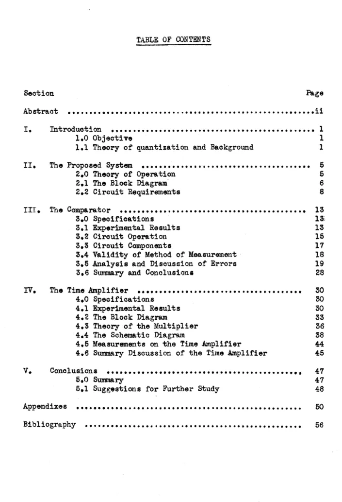
employing a diode selector and regeneration for high gain in amplify-ing the break characteristic. The schematic diagram is shown in Fig.3.
That this circuit meets the specifications set up as regards
stability and short and long range drift is shown by the graph (Fig.2 )
-14-I"
iL jJI 2 I-... U ' IaO '-I-0 0 O E: g ILL C.. I-. IL 0 A o No o JjVIIOA :3,'v3s!:n llt_- -0 N33•~d : -:! is
S11_ ' I L3 1"Vn.LV WO)d: A:lXVi'9 d,.LLV ONI•AO NOI.LVIAIA
-'- i i 0 oc uI u. --LI
r
ii
I
Cf :: 0.5:
OO:V
-IV
00;5
sl :j7o
1 0oo~t
5
.vs
.%~:I 0* o*:i
I*oo~b:s
.Q: jTZ * 'Z uI o n t--<c \ -r o L,) LL I--cO u-iuji
difference between a fixed reference voltage and a variable voltage vhen the comparator indicated equality of the two. This is plotted as a percentage of full scale voltage. Each point plotted represents a
series of from ten to twenty-five sueessive reading taken at the time indicated on each particular day of the three days on which data was taken. Both the average reading and the maximan excursion to either side is shown since the accuracy depends upon each reading being within the specified bounds, - .05 volts. It can be seen that the bounds are in no case exceeded.
5.2 Circuit Operations
The action of the Multiar circuit may be explained as followsr The pentode normally is conducting with approximately zero bias and is drawing slight grid ourrent through the grid resistance, The diode is: not conducting sinee the sweep voltage is initially positive with respect to the referenoe voltage. As the sweep voltage goes negative it approaches the value of the reference and the diode begins to conduct. The
oon-duotion of the diode puts the pulse transformer winding 1-2 in the
circuit. More important, it causes a slight negative voltage to develop at the grid due to conduction through R. Because of the Gm, of the tube, this slight negative voltage is amplified at the cathode Thich feeds the amplified negative voltage back to the grid through the pulse trans-former with a 2:1 step-up ratio. This regenerative feedback causes aL sharp negative drop to appear at the grid of the pentode, driving it below cutoff. The time constant of the transformer winding causes the
-16-toeward the original condition aided by regeneration. As the grid voltage approaches zero, the sweep voltage takes over to cause the grid to start downward again. This "bouncing" will continue until the sweep voltage has decreased to the point where the tube is cut off. These multiple pulses are not disadvantageous since the comparator output pulse is used to trigger two multivibrators which are insensitive to any but the first trigger. Rise time of the output pulses is 0.5 microseconds.
FIG. 3. COMPARATOR
3.3 Cirouit Components r
Sinee precise operation is required of this circuit, the components are necessarily chosen for close tolerances and low drift coeffecients. One percent wire wound resistors were used in all cases. Actually the resistors do not need to be very close to their indicated value, it is far more important that they have, low drift, low noise, and low temper-ature coefficients. The capacitors are not at all critical since they are used in this circuit for coupling or by-passing only. The pulse transformer used was the Westinghouse 134 BWF which has the very good high frequency response required to deliver a fast rising output pulse.
The pentode used in this circuit was the 6 SG7, but other types, namely the 68H7 and the 68J7, were found to work equally well. The requirements on this tube hare that it have a high grid to cathode transoonductance and small aging effects. Since the tube is operated at zero bias, the transconductance is fairly constant over small changes in tube current.
The most oritical element in the circuit is the diode. It operates as the selector, the rest of the circuit is concerned with.amplifying its "broken-line" characteristic. The type 6AL5 was chosen for this application because of its low foreward resistance, stability,and low interelectrode capacitance. A further discussion of the diode charac-teristies may be found in the discussion of errors, seotion 5.5.
It is apparent that other types of circuits may be used to perform
voltage comparison. Different types of selectors such as germarbiaum crystals or triodes may be used. Multivibrators or blooking oscillators or ordinary amplifiers may be used to provide gain. Some of these
-18-possibilities as well as further discussion of the reasons for choosing the Multiar for this application may be found in the Appendix, section VI.
5.4 Validity of Method of Measurement:
Before proceeding with analyses of the circuit operation and the experimental results obtained, it might be well to establish the validity of the method of measurement employed.
The circuit used for all the measurements of drift, stability, and circuit dependence on parameter drift is shown in Fig. 2. A voltage divider with a constant current of 10.00 milliamperes flowing through it was provided to supply a fixed and a variable voltage to the Multiar to simulate the function to be coded and the sweep voltage respectively. (The current through this divider was maintained constant by manual adjustment.) Resistor RI was varied so that the variable voltage
approached the fixed voltage. Apparent equality of the two voltages was indicated by an output pulse from the Multiar which was fed through a cathode follower to an oscilloscope where it was used to trigger a driven sweep. The sweep speed of the oscilloscope was set to be slow enough that a single sweep was visible. Thus a single output pulse
could be detected. The output pulse was positive, 18 volts in amplitude, with a rise time of 0.5 microseconds and a duration of 2.0 microseconds.
In lieu of the negative going sweep having a fall rate of about 0.5 volts per microsecond which would be applied in actual operation, the variable voltage mentioned above was provided. This voltage was actually applied in quantized form since R1 was a decade resistor.
It is necessary to show that the results obtained with this variable
voltage applied do not differ significantly from the results Vhieh would be obtained if the actual sweep were applied.
With a diode capacity of 3.2 uuf and an assumed stray capacity of about 2.0 uuf, the input time constant is seen to be only .05
micro-seconds. Since the rate of change of the sweep voltage is so low, it might be expected that the dynamic characteristic of the Multiar will not differ greatly from the static characteristic.
Quantized steps of .01 volt were used after it had been established that steps of .001 volt applied did not alter the apparent coincidence
point. To further insure that a switching transient was not responsible for the triggering, an R-C filter was inserted in series with the
variable voltage supplied to the Multiar. It was found to cause no appreciable change in the coincidence point. It is apparent that once
the current through the diode is increased beyond a certain point, the circuit operation is sensibly independent of the applied variable voltage.
The readings for the graph previously presented, (Fig.2) were taken with the diode filament voltage manually regulated to be 6.0 1 0.1 volt me for reasons to be discussed subsequently in Section 3.5.
3.5 Analysis and Discussion of Errors:
Analysis of the Multiar circuit operation is complicated by the fact that the diode and the grid circuit of the pentode are extremely nonlinear in the region of operation. The diode changes its effective resistance from nearly infinity to 200 ohms along an exponential
characteristic. 4 The grid resistance of the pentode changes its
7
-.20-resistanmee from a few thousand ohms to practically infinity during the first part of the trigger action. These variable resistances eomplicate
an analysis of the cirouit on the basis of feedback amplifiers. On a qualitative basis it is apparent that if the characteristic of the diode is exponential, no combination of its characteristic with linear elements will sharpen the break. It is also apparent that any element which
inhibits the feedback path or reduces the gain in this path will cause the required voltage increment across R to be larger to initiate the regenerative action, thus changing the effective coincidence point.
Because of the difficulties mentioned above, the analysis of the oirouitk operation was earried out on an experimental rather than a theoretical basis. To this end, various parameters in the cirouit were varied and their influence on the apparent coincidence point established. In some instances resistances were ainserted in the circuit to simulate changes in tube parameters.
For mall changes in parameter, the deviation in apparent coinoi-denee point is a linear function of the parameter. For this reason the influence of a change in any parameter on the apparent ooineidenoe point is independent of the setting of the other parameters. Several tests were conducted to insure that this was the case.
The curves for various parameter changes are plotted on a graph (Fig. 4). Since the slope of the curves alone is of importance, the plot is of the percent change in apparent coinoidenoe with the parameter variation. The circuit is redrawn showing the insertion of variable resistances. In each case all but one of the inserted resistors were
-21-EDUALITY FROMBRTUAl FOUALITY IN CIRCUIT PARAMETER
I
I0
c~Z±K2
Rsp
INSERTED SERIES SCREEN GRID RESISTANCE Rsp-KILOHMS
o 2.0 4.0 6.0 ao0 0
INSERTED SERIES GRID RESISTANCE R-- KILOHMS
0 *a0 .40 .40 0o 1.0
INSERTED SERIES DIODE RESISTANCE Rý- KILOH1MS
0 .05 .10 )S' ,20 .25
INSERTED SERIES CATHODE RESISTANCE R -- KILOHMS
7,0 6.6 G.2 5.8 5.4 5.0
DIODE FILAMENT VOLTAGE -RMS VOLTS
FIG.
4.
I-4. Luj
jr · w--I E ": -.1 CD >LL >- _1.i
D LL LsJj t - LL uJ Lu I-LU ... w. ,m,, , v i • • T k t i---ii
ii -:1:
::- .:I:
---
:r
L i; hz
-22-set to sero to eliminate interdependence. Note that the resistance scales are not identical since the effectiveness 6f resistance change depends upon the percentage change rather than absolute change at different parts of the circuit.
Before discussing each individual curve it might be well to point out that another factor not previously mentioned is of importance here. This is the dispersion of suocesive readings for a given condition. The dispersion indicates the stability of the coincidence indication for any particular set of circuit conditions. The average value of the readings for any point on a curve has no significance unless the range of readings is sufficiently small to insure that extraneous random causes are not affecting the readings. In short, the results must be interpretable through the "noise" of random effects.
In the case of each curve plotted (Fig.4), the points plotted are the average of 5 readings whose dispersion was not more than .01%.
A.s might be expected, changes in some of the parameters causes a change
in dispersion of the readings as well as a change in the average reading. This is true of the pentode plate load resistor and of the transformer ratio. For this reason, the plate load resistance was set at effectively zero ohms and the transformer ratio was set at the low ratio of 2:l. The diode load resistor R was set at a fairly low value, 10,000 ohms, for the same reason. For all the other components, the dispersion increase was not significant over most of the range of variation.
The effects of parameter variation may be summarized in a table of coefficients giving the slope of the curve for each parameter. Attention should be paid to the units given for each coefficient since
the relative importance of each parameter's variation depends upon both the coefficient and the probable variation of the parameter.
Parameter Varied Effect
Filament voltage .17 percent
fil. volt-rms.
Pentode load (negligible)
resistance
Plate supply voltage (negligible) Screen Resistance -. 01 percent
(inserted) kilohm
Control grid series
resistance (inserted) -. 05 percent kilohm Diode series resistance -.17 percent
(inserted) kil ohm
Cathode series resistance -.90 percent
(inserted) kilohm
The effect of filament voltage variation has proven to be of greatest importance. While the coefficient does not appear to be very large, fluctuations of a few tenths of a volt in filament voltage are not uncommon in general practice. As a matter of fact, it is difficult to regulate the filament supply voltage manually to within a tenth of a volt with the aid of an ordinary a-c meter covering the necessary voltage range. This means that about .02% random variation may be expected on the drift record (Fig.2). Aging effects may be considered together with filament voltage drifts because the effect is the same, the cathode temperature changes.
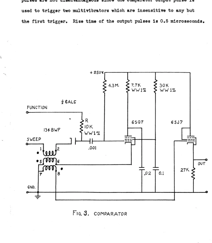
Because of its great importance, it might be well to consider the mechanism of drift due to filament temperature change in a diode. (The
filament temperature effects in the pentode are negligible in the region of normal operation of the tube.) The sketch shown in Fig.6 is the low current characteristic of a typical 6AL5 diode plotted on a sermn-loga-rithmie scale. The fact that the curve
is approximately linear shows that the current is an exponential function of the voltage across the tube. We may consider that the multiar circuit triggers with a certain voltage across the diode load resistor, R, each time. In other words, the diode current for triggering is constant. Therefore, a filament temperature change is
equiva-Il
t4 & IUC1^'&t h&Ut -& '&1 'L& lfor right along the voltage scale. The FI6.5- DIODE CHARACTERISTIC voltage applied to the diode circuit to effect triggering is therefore a function of cathode temperature.
It is apparent that some sort of regulation must be applied to the filament current of the diode for accurate operation of the circuit. Use of a regulator such as a carbon pile with direct current or a sat-urable reactor with alternating current v ll be necessary in this circuit.
As an alternative or perhaps as a further aid, the cirouit of Fig. 6a
4-25
Compensation is provided by the two diodes generating equal voltages dependent upon the filament temperature with opposite polarity. The diodes should be in the same envelope and be matched for best results. An equivalent circuit is shoen in Fig.6b. It may be pointed out
how-ever, that addition of eapacitance across resister R is undesirable since it adds a transient effect when the sweep voltage is used. Another important point is that noise generated in the compensating
diode may trigger the circuit near the coincidence point. Measurements made with this oirouitwere inconclusive. The dispersion of readings
at each point was much higher than could be tolerated, but the curve itself showed anomalies. Lack of time prevented further investigation.
It is possible that the method of measurement was at fault. This circuit merits further investigation.
uJLv
(a)
(b)
FIG.
G.
DIODE COMPENSATION
The coefficient associated with the variation of an inserted series screen resistor is of little importance in itself but it does have an important implication; the transoonductance of the amplifier tube may
-26*•
Below a certain point, however, the effective coincidence voltage changes radically and the triggering is speasmdic. In short, a certain minimum
grid to cathode transeonductance is necessary for normal operation but an increase over this minimum benefits circuit operation little. This
is highly desirable since it means that aging effects in the pentode may be virtually ignored. This is due to the fact that regeneration is
used, making the rise of the output pulse dependent only on the physical circuit time constants.
The other three resistors varied are all in the regenerative loop and their influence on circuit operation may be expected to be greater. The effect of adding a series control grid resistance, though greater, is also of minor importance. From the circuit of Fig.4 it can be seen that the effect is to add a voltage divider circuit consisting of the inserted resistor and the conducting grid resistance shown dotted. The effective grid characteristic is changed only in the positive grid region of the output pulse and so the change is of little importance. No simple way of changing the grid characteristic of the tube was found. To
simulate the shifting of the grid current-voltage curve along the voltage
axis, a voltage was added in series with the grid but variation from
-2 to - 2 volts produced no change whatsoever. The fact that the grid is supplied through a large series resistor to the plate supply pro-vided automatic adjustment of the grid bias to the correct value.
Inserting resistance in series with the diode may be considered to be the same as increasing the resistance of the diode at the point where effective coincidence occurs. A certain current must flow
2
resistance to drop drastically. The gain around the loop is the product of the gain from the cathode to the grid and the gain from the grid through the tube to the cathode. Assuming the transformer to be ideal, the cathode to grid gain is simply
2
. 2R - 1 FIG. 7. EQUIVALENT CIRCUITek R+ ra +rd
where rjais the inserted resistance and rd is the dynamic resistance of the diode. When i' is increased, rd must be decreased to make the
loop gain equal to one, To accomplish this, triggering must occur on a different part of the diode characteristic where the dynamic resistance
is smaller.
This part of the investigation illustrates the effect of a change in the shape of the volt-ampere characteristic of the diode. It is felt that such changes will be small enough to be virtually ignored because the shape of the diode characteristic in the low current region
K
-27-in series with the diode a higher voltage is required to supply this current.
Another way of looking at this condition is illustrated in Fig.7, below. The equivalent feedback circuit is shown with the diode re-placed by a variable resistor,rd. Effectively, the diode starts out at infinite resistance and reduces its resistance until the gain around
-28-is essentially an exponetial dependent upon the distribution of velocities in a cloud of thermally excited electrons and the tube geometry neither of which change with age.
Reference to Fig.7 makes clear the reason for the large effect of increases in the cathode resistance. The unbypassed cathode resistor
simply causes degeneration, reduotag the gain from the grid to the transformer terminals in the cathode circuit. As a consequence, the diode must be at a lower resistwace point on its characteristic when triggering occurs. Ordinarily the only resistance in the cathode is that of the transformer primary thich in the case of the Westinghouse 134 BWF is about 10 ohms. This resistance does not change appreciably even over long periods of time, and does not change significantly with temperature.
,.6 tummary and Conclusionst
The preceeding exposition establishes the Multiar circuit as suitable for operation in a circuit with a resolution of one part in a thousand. Figure 4, which shows drift over a period of three days represents the results of optimization of the circuit parameters. The drift was within the required bounds for operation with 0.1% accuracy.
The chief cause of inacouracy has been shown to be filament
temperature drift in the diode. It is possible to conclude that other causes of drift are relatively insignificant over short periods of time
and may be calibrated out ever long periods of time. This is provided, of course, that suitable precaution is taken in construction to insure that components have low noise and low thermal coefficients and are
m29
stable over long periods of time.
Both compensation and filament voltage regulation will be necessary for dependable operation of the Multiar. The fact that the circuit uses regeneration makes it unnecessary to provide gain regulation and makes the circuit relatively insensitive to the characteristics of the pentode, In other comparator circuits where regeneration is not used, changes in characteristics of tubes other than the diode will cause instability and drift..
ii: --- · · · ... ... :. - ---- -... ..... .-- I---~-.- -I
Section IV
The Time Amplifier
4.0 Specifioations:
Reference to section II, The Proposed System, indicates that basically the Time Amplifier is required to recognise and measure a time interval of from 0 to 12 microseconds and to deliver a pulse which has a length 32 times the input time interval minus 12 microseconds. When the input pulse is ..375 microseconds, the output pulse is of zero width. For smaller input time intervals the output pulse must be zero also. The equation governing the action of the time amplifier ist
To - •2Ti - 12 microseconds.
4.1 Experimental Resultsl,
Figure 8 is a plot of the experimental results obtained in testing the time amplifier circuit designed for application to this quantizer..
The duration of the output gate pulse is plotted as a function of the input time interval. The points are actual readings, but the line drawn through them is the theoretical equation given above. It is not useful in this case to obtain the best line through the points because the
readings have significance only with respect to the theoretical curve. The ~sriations of the readings from the theoretical curve are also plotted together with the allowable limits of error.
-31-nllITuIT 2A-EI" Dilt C" I iIDATItM Ae A ikt-Ilr-fir~kL
t-INPUT TINE INTERVAL - MICROSECONDS
FG..
J.
E.
G.
4/12 /51I z 0 ILI u~l 0 I--C) 1 LutH I-0I 0 o +1 Of w~
-52-12. microseconds, the allowable limits of error are plus and minus 6 micro-seconds, A certain experimental uncertainty arises from difficulty in measuring the input time interval. It was estimated that the uncertainty in this measurement was .1 microsecond at a minimum so the uncertainty in the output pulse was at least 3,2 microseconds. The average error was -2 microseconds showing that perhaps the calibration of the circuit was not exactly correct.
The additional functions of the time amplifier circuit are more or less incidental to the multiplication process. The readout and reset signal is simply the trailing edge of a monostable multivibrator pulse which is used to switch a sweep circuit on. The so-called crossover problem must be handled somewhat more extensively. The effect in question is the possibility of a 12 microsecond pulse being counted by both the coarse count circuit and by the fine count interval measurement circuit, due to its finite width. The problem will become more clear when the precise mechanism of measurement is discussed later in this section. At that time the proposed treatment of the problem will be fully explained.
The input time interval is marked by two pulses. The beginning is signified by the comparator pulse and the end, by the next coarse count pulse. Each of these pulses has a finite width and a certain rise time. To effectively delineate the interval of time, the Time
Amplifier must be triggered by the same point on each pulse each sampling period. A constant time lag may be calibrated out but jitter in the difference between pulse times must be limited to less than the interval corresponding to a fine count, namely .375 microseconds. It must be
remembered that this jitter appears in the output pulse multiplied by 32.
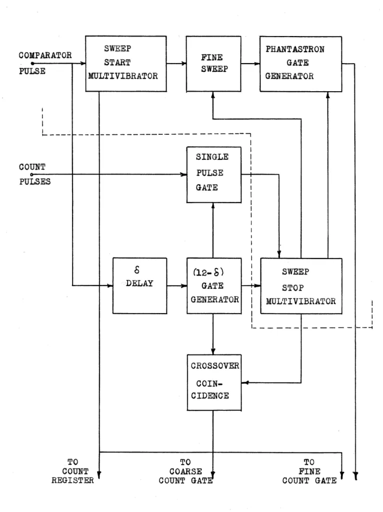
4.2 The Block Diagramxt
The block diagram (Fig. 9) must be referred to at this point to facilitate explanation of the operating principles of the Time Amplifier.
Only that portion of the block diagram blocked off by the dotted line was constructed and tested. This section contains the input interval measurement, the multiplication and subtraction, and the gate pulse
generating circuits. It will be possible to discuss the operation of this section in more detail in the presentation of the schematic diagram. At that point the significant waveforms produced in this part of the
circuit will be reproduced to aid discussion.- For the present the action of the overall Time Amplifier circuit will be discussed..
To initiate the action of the Time Amplifier the comparator pulse triggers the Sweep Start Multivibrator, which is monostable. It supplies
a negative pulse with duration slightly longer than the maximum possible
fine count gate width to the Fine Sweep circuit causing the sweep to start. The comparator pulse also goes through a delay ofc , equal to the width of the coarse count pulses, to trigger another monostable multivibrator, the (12 -6 ) Gate Generator. TheS Delay is supplied by any simple fixed delay circuit and is necessary to the operation of the Crossover Coincidence circuit but not of importance to the basic operation of the Time Amplifier. The (12 - S) Gate Generator generates a fixed gate of width (12 -6) mieroseconds which is applied to the
Single Pulse Gate which in turn gates one of the count pulses through it to trigger the Sweep Stop Multivibrator. The Sweep Stop Multivibrator
-34-Fig. 9. TIME AMPLIFIER BLOCK DIAGRAM
--- 4
;;--supplies a positive pulse of approximately the same duration as the sweep jstrt pulse to the Fine Sweep circuit to stop the fine sweep and to hold the sweep voltage at the value it has attained. This voltage is directly proportional to the input time interval.
The leading edge of the Sweep Stop Multivibrator pulse is differ-entiated and applied as a trigger to the Phantastron Gate Generator to trigger it on. Meanwhile, the attained value of the Fine Sweep voltage
is applied to the Phantastron Gate Generator to set the starting point of the phantastron sweep. The starting voltage of a phantastron sweep generator determines the total time of sweep, since the rate of sweep and the ending point of the sweep are fixed. The duration of the sweep is the same as the duration of the screen voltage pulse which is used
as the fine count gate. It appears,then, that the Phantastron Gate Generator produces a pulse width proportional to the value of voltage
fed in from the Fine Sweep. Subtraction of the 12 microseconds is also performed in this part of the circuit but the mechanism of this will be discussed later.
If the comparator pulse were by chance exactly coincident with a coarse count pulse, the beginning of that coarse count pulse might be
fed into the coarse count register. If then the delay of one pulse
width were not provided before opening the Single Pulse Gate, the
trailing end of that same pulse might pass through and trigger the Sweep Stop Multivibrator. This would result in a zero fine count when a
maximum fine count is desired since the Fine Sweep would be immediately turned off when it should have been allowed to run until the next
85*36
count pulse appeared. Introduction of the 6 Delay introduces a new
problem, however. If the comparator pulse occurs just before a coarse
count pulse, the coarse count pulse would occur entirely within the
delay time and would not appear in either the coarse count register
or-in the Sor-ingle Pulse Gate. As a result, the Sweep Stop Multivibrator would not be triggered at all. To eliminate this trouble, the trailing
edge of the (12 -4 ) gate pulse is arranged to trigger the Sweep Stop Multivibrator if it is not already on. Triggering the Sweep Stop
Multivibrator at this time means that the last coarse count pulse should have been counted in the coarse .count register. To supply this coarse count the Crossover Coincidence is arranged to feed a single pulse through the Coarse Count Gate eireuit whenever the Sweep Stop Multivi-brator has been triggered by the trailing edge of the (12 -6) gate.
A more detailed consideration of the crossover problem together
with the proposed circuit design to eliminate the difficulty may be found in the Appendix, Section VI of this report.
4.e Theory of the Multipliers:
Before plunging into the details of the physical circuit it will be well to investigate the theory of the computation accomplished in the circuit. It has already been described how the Sweep Start and the Sweep Stop Multivibrators allow the Fine Sweep to attain a certain voltage ahich is held, and how the Phantastron produces a sweep which
starts at this voltage and ends when it reaches another constant voltage. The sketches shoem in Fig. 10 and the following algebraic derivation
m37-show how the ccmputation is accomplished using the characteristics of the circuits, SWEEP START
'svFE EP
F a.b1
c
S
_-_---
-- -- -
iP--05 S- (V,-c -)
FIs.
10.
TIMEMULTIPLICATION
INE
WEE P
HANT. WEEP
t i - Input time interval
- Unavoidable time delay in one or both input
pulses
a - Rest position of the fine sweep in volts b - Sweep rate of fine
sweep in volts/T see, vI - Attained voltage of
fine sweep
d - Inital step in phant-astron sweep in volts e - Ending voltage of
phant-astron sweep in volts k - Reciproeal of phantastron
sweep rate in p seco/volt to - Duration of output gate
V1 - b(t i + )+ a volts
to
a
k(vl -c
- d) p see.to - k(bti + bA + a - c - d) sec.
to - kbti + k(bŽe + a - o - d) 1 see, kb = 32
k(b
a - c-d) a -
12
p see.
to : 32t i - 12 ) sec.
-88-The constants and (d) are fixed by the circuit parameters used and in practies (a) will be set &t a fixed value also, though it is theoretically variable. The sweep rates (b) and (1/k) as well as the Phantastron sweep ending voltage, (c), are continuously variable and may be set to satisfy the two conditions specified. It will be conven-ient to simplify the settings even further by arbitrarily setting (b) at a convenient value and providing for calibration by variation of the phantastron sweep rate (!_) and ending voltage (c).
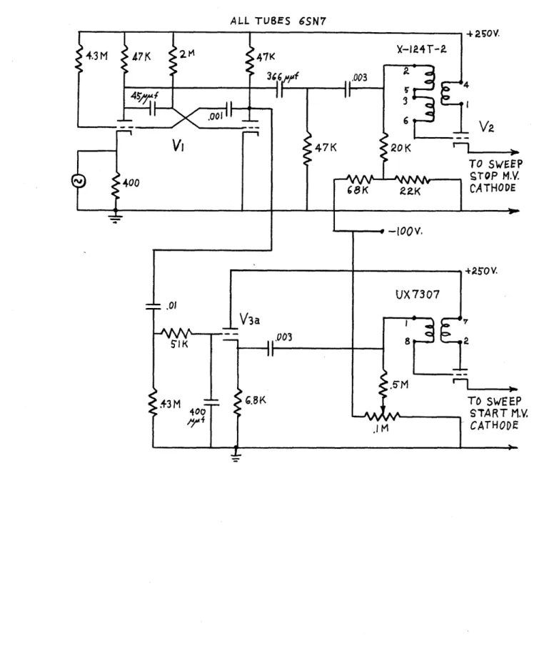
4.4 The Schematic Diaramt
The schematic diagram of what may be termed the "computing"
elements of the Time Amplifier circuit is shown in Fig. 11. Fiýurie12 is a chart of the waveforms produced in the circuit. The drawings are reproduced from tracings of the actual oscilloscope pattern made with the aid of an Oscillotracer. Both the entire waveform aund an expanded view of the leading edge of each waveform is shown. The actual period
of the waveforms in 996 microseconds but only the portion shown here
is of interest since the remainder of the period is recovery time. The
waveforms will in general be different each sampling cycle since the fine count will fluctuate rapidly vith slight changes in the input
function. The waveforms shown here are for an input interval of approximately 10 microseconds corresponding to an output pulse width
of approximately 308 microseconds.
For the time being we shall assume the proper triggers fed into the Sweep Start and Sweep Stop circuit. The circuits used to generate these pulses are discussed in the Appendix. As may be seen from the
--
-39-CL.
-40-SWEEP START TRIGGER
SWEEP STOP TRIGGER
SWEEP STOP TRIGGER
-IN
SWEEP START MULTIVIBRATOR
In
r "11 3WrCc r" I
PHANTASTRON SWEEP
FINE COUNT GATE PULSE
11= 200 sEc. AMPLIF(ER WAVEFORMS I i
n_
I ,i1"=
IOPSEC.FiG. 12.
TIMEI
1I
the chart of waveforms (Fig.12) the input triggers are of about 1.5 microsecond duration.
The trigger to the sweep start multivibrator, V1, is fed in on the cathode of the normally conducting tube, flipping the monostable multi-vibrator to the abnormal state. Its timing circuit keeps it in that state for approximately 400 microseconds at which time it flips back to its normal state. The waveform taken from the plate of the normally off tube is a negative rectangle of 400 microseconds duration which is used to out off VIO, normally at zero bias. The expanded view of the sweep start trigger and sweep start multiVibrator waveforms shows that the multivibrator is triggered by the leading edge of the trigger with negligible delay. It should be noted that although the multivibrator waveform is not perfectly square, only the first 10% of the drop is
actually used to cut off VIO. A similar situation exists for the sweep stop waveform.
Tubes V9b, VlO, Vlla, and V12 comprise the Fine Sweep Generator. The circuit is basically that of a bootstrap linear sweep generator* with the exception that V9b is inserted in the sweep rate determining network composed of R30 and C14. Since V9a is cut off in the normal
condition,the grid of V9b is tied to the plate supply through R27 and V9b is drawing slight grid current to maintain itself at a slight
positive bias. The chain VI0, V9b, and Vlla is conducting, holding the voltage on C14 down to a low value, approximately 25 volts. When V10 is out off by the sweep start pulse, the circuit acts like an
ordinary linear sweep generator. Tube V9b acts as though it were a
* See Sec. 7 and 8 of Ref.4 for a discussion of bootstrap sweep generators.
resistor with a value equal to its static resistance. For the 6SN7 operated at slight positive bias, the static resistance is practically equal to the dynamic resistance. This means that as the grid to cathode voltage changes slightly during the sweep, there will be practically no effect on the linearity of the sweep. This is important because as the
cathode voltage of V9b rises with the sweep, the voltage across R27 changes, changing the grid current drawn from V9b. A change in grid current produces a change in grid to cathode voltage which in turn changes the effective static plate resistance of the tube. Briefly, then, V9b acts as a "grid follower" and essentially remains a constant resistance so that the Fine Sweep Generator generates a linear sweep when triggered on by the Sweep Start Multivibrator.
The triggering action of the Sweep Stop Multivibrator is identical to that of the Sweep Start nMultivibrator. In this case, however, the positive going waveform is used. It is used to turn on V9a mhich is normally just below cutoff. The waveform at the grid of V9a is clamped positive with respect to -100 volts so that only the first 20% of the rise of the multivibrator waveform is used to bring the tube into the positive region. When V9a conducts, its plate is immediately driven negative to some value below ground. This will out off V9b no matter what part of the fine sweep it is on because the cathode of V9b is held to the attained sweep voltage by C14. With V9b cut off C14 has no discharge path and so holds its charge until either VI0 or V9b again conducts. Neither of these tubes will conduct for about 400 microseconds until both the sweep start and sweep stop voltage pulses are ended,
7·nTa--43..
at which time the entire Fine Sweep Generator returns to normal, The fine sweep waveform illustrates the precise operation of the circuit -which is linear to within 1,0%. The jitter in turning the Fine Sweep Generator off and on is so small it vas not discernable on a 0.5
micro-second per centimeter oscilloscope display.
The waveform of the Fine Sweep Generator is fed to the Phantastron plate through a diode for isolation. The Phantastron is a conventional
screen coupled phantastron circuit and needs little comment.* When it is triggered on it generates a linear sweep starting at whatever voltage the plate happens to be set at, with a sweep rate set by the values of
RI0 and C5. The sweep ends t~en the plate voltage becomes so low that diode V2b conducts, holding the plate voltage at the voltage set on R8. This adjustment is that described in Section 4.5 as voltage (c) and determines the constant time subtracted during multiplication, in this case 12 microseconds.
The Phantastron is triggered in the following mannert. A negative going rectangle from the Sweep Stop Multivibrator is amplified and inverted in V1S, differentiated by C17 and R37, and applied to the
suppressor of the Phantastron through a diode, V6a. Since this trigger occurs a fraction of a microsecond after the sweep is stopped and since the sweep is stopped by a coarse count pulse triggering the Sweep Stop Multivibrator, the Phantastron sweep is started just after a coarse count pulse. The importance of this will become apparent subsequently.
As has been previously pointed out, the screen voltage of a
Phantastron sweep circuit exhibits a positive pulse for the duration of the sweep. This pulse is used as the fine count gate shown in the last
m
-44-waveform of Fig.12. This -44-waveform shows that a spurious pulse is also generated. This spurious pulse is caused by the Phantastron being triggered by the negative drop of the fine sweep waveform applied to its plate. This is not serious, however, because the waveform of the Sweep Stop Multivibrator may be used together with the fine count gate pulse generated by the Phantastron cirouit in a double coincidence circuit to actually gate the fine count.
The small negative step of the Phantastron screen voltage is due to the linear rise applied to the plate of the Phantastron being applied to the control grid through the cathode follower VSa and capacitor 05. The diode V4 has been provided to .limit the positive
step on the control grid, thereby limiting the negative step on the screen.
It was pointed out above that the Phantastron sweep is started just after a coarse count pulse. This means that the fine count gate
starts just after a coarse count pulse. For this reason the same train of pulses 12 microseconds apart may be used for the fine count as for the coarse count.
4.5 Measurements on the Time Amplifier:
Measurement of the characteristics of the Time Amplifier circuit were carried out by making measurements of the input time interval between pulses and the output pulse width using an oscilloscope trace with externally generated time markers superimposed upon it. The time markers were obtained from oscillators previously calibrated against a
crystal oscillator. Readings of the input time interval were made
.. .n..-...
r--r-.-~--r----using 1.0 mierosecond markers except that those intervals in the range of from 0 to 3 mieroseonds were measured using 0.2 microsecond markers. Measurement of the output pulse was made with the use of 5 microsecond markers.
It was not possible to measure the input time interval to an accuracy of greater than 0.1 microsecond with the equipment available.
This is an accuracy of one part in 120 or about 1.0%. The output pulse time was even more difficult to measure directly in this manner because of the small marker spacing compared to the pulse width. Due to
difficulties connected with the finite rise time and fall time of the output pulse and the limit on sweep speed necessary to view the entire waveform, measurements of the output pulse width could be made to about half a marker interval or about 3 microseconds. Since the output pulse
had a paxidmum time of 372 microseconds, it could be measured to an
accuracy of about 1.0%. The overall accuracy of measurement was of the order of 2%.
The circuit used to generate the trigger pulses used for the test is of minor importance so long as it can be demonstrated that the pulses meet the requirements as regards rise time and jitter. Measurements
of the input time interval established that they did meet requirements. For the sake of completeness, however, the circuit actually used is described in the Appendix.
4.6 Svmmar Discussion of the Time Amplifier:
Although only the "oeemputational" elements of the Time Amplifier were constructed and tested, it is felt that the validity of this method
-'464-has been proven since the remaining circuits may be of conventional design. Suggested designs for the remaining circuits of the Time Amplifier are given in the Appendix where the so-called erossover
problem is diseuesed.
The accouracy that this eircuit is required to maintain is one count in 32 or about 3%. The method of measurement admitted of an accuracy no greater than about 2%. In all probability, then, the errors plotted in Fig. 8 are pessimistic. Measurements were taken over a period of a week and no evidence of instability either over
short or long periods of time was found. (By instability is meant drift outside the limits of error.)
Short of building the entire quantiser, there is little likelihood of measuring the action of the Time Amplifier except with an effectively constant input. The cirouit recovers completely during each esyle, however, making each oycle of operation independent of previous cycles.