Publisher’s version / Version de l'éditeur:
ECS Transactions, 33, 33, pp. 17-36, 2011
READ THESE TERMS AND CONDITIONS CAREFULLY BEFORE USING THIS WEBSITE.
https://nrc-publications.canada.ca/eng/copyright
Vous avez des questions? Nous pouvons vous aider. Pour communiquer directement avec un auteur, consultez la
première page de la revue dans laquelle son article a été publié afin de trouver ses coordonnées. Si vous n’arrivez pas à les repérer, communiquez avec nous à [email protected].
Questions? Contact the NRC Publications Archive team at
[email protected]. If you wish to email the authors directly, please see the first page of the publication for their contact information.
Archives des publications du CNRC
This publication could be one of several versions: author’s original, accepted manuscript or the publisher’s version. / La version de cette publication peut être l’une des suivantes : la version prépublication de l’auteur, la version acceptée du manuscrit ou la version de l’éditeur.
For the publisher’s version, please access the DOI link below./ Pour consulter la version de l’éditeur, utilisez le lien DOI ci-dessous.
https://doi.org/10.1149/1.3578018
Access and use of this website and the material on it are subject to the Terms and Conditions set forth at
Bringing silicon to light : luminescence in silicon nanostructures
Lockwood, David J
https://publications-cnrc.canada.ca/fra/droits
L’accès à ce site Web et l’utilisation de son contenu sont assujettis aux conditions présentées dans le site LISEZ CES CONDITIONS ATTENTIVEMENT AVANT D’UTILISER CE SITE WEB.
NRC Publications Record / Notice d'Archives des publications de CNRC:
https://nrc-publications.canada.ca/eng/view/object/?id=1ffd4d6b-0651-4283-b62f-6f182049cecd https://publications-cnrc.canada.ca/fra/voir/objet/?id=1ffd4d6b-0651-4283-b62f-6f182049cecd
Bringing Silicon to Light: Luminescence in Silicon Nanostructures
David J. Lockwood
Institute for Microstructural Sciences, National Research Council, Ottawa, Ontario K1A 0R6, Canada
The many and diverse approaches to materials science problems have greatly enhanced our ability in recent times to engineer the physical properties of semiconductors. Silicon, of all semiconductors, underpins nearly all microelectronics today and will continue to do so for some time to come. However, in optoelectronics and, more recently, in photonics, the severe disadvantage of an indirect band gap has limited the application of elemental silicon. Here we review a number of diverse approaches to engineering efficient light emission in silicon nanostructures. These different approaches are placed in context and their prospects are assessed for applications in silicon-based photonics.
Introduction
The ubiquitous silicon microelectronics “chip” is taken for granted in modern society. There has been much research involved in producing these high technology marvels and such research continues unabated at a faster and faster pace. Despite the often stated announcement that “the age of GaAs has arrived”, it never quite has, and continued developments in Si and, more recently, Si1-xGex alloy/strained Si technology (1-3) continue to advance the frontiers of microminiaturization, complexity, and speed. This continued advance has been driven by application requirements in switching technology (e.g., computers) and high-speed electronics (e.g., wireless telecommunications). Gallium arsenide and other compound semiconductors have, however, maintained a significant role in the construction of optoelectronic and purely photonic devices where the medium of switching and communication is light itself (4).
The merging of Si-based electronics with photonics has largely required the pursuit of hybrid technologies for light emitters and modulators (see, for example, Ref. 5), which are often both expensive and complicated to produce. The most satisfactory solution and still mostly a dream as far as electrically-pumped light sources are concerned would be optoelectronic devices created entirely from Si-based materials, where the extensive experience in Si fabrication and processing could be put to best use. Already, a wide range of optoelectronic integrated circuits (OEICs) incorporating Si or Si1-xGex as a detector or waveguide have been elaborated (1,5-10). Despite these advances, the major deficiency in Si-based optoelectronic devices remains the lack of suitable light emitters and especially lasers.
The general requirements in Si-based light sources are efficient light emitting diodes (LEDs), lasers, and optical amplifiers for use in optical communications technologies such as fiber optics and displays. Operating wavelengths in the range 0.45–1.6 µm are needed to cover both full-color displays and the fiber-optic operating wavelengths of 1.3 and 1.55 µm. Specific applications for such sources include fiber-optic transmitters, optical interconnects within and between computer chips, information display screens,
printing elements in xerography, and writing and readout of optical compact disc information.
Many quite different approaches to alleviating the miserable light emission in bulk Si (~10-4 quantum efficiency at 300 K) have been proposed and are actively being explored (11-16). Some, such as Si1-xGex quantum well or Si/Ge superlattice structures, rely on band structure engineering, while others rely on quantum confinement effects in low dimensional structures, as typified by quantum dots or porous Si [π-Si (17)]. Still another approach is impurity-mediated luminescence from, for example, isoelectronic substitution or by the addition of rare earth or transition metal ions. An overview of results obtained with some of these methods is given below with references to the primary sources for each development. However, in order to understand more fully the reasons why such different approaches are necessary, it is appropriate to review first what creates the optical emission problem in crystalline Si (c-Si).
Optical Emission in Silicon
Silicon crystallizes in the diamond structure (18), which consists of two interpenetrating face-centered cubic lattices displaced from each other by one quarter of the body diagonal. In zinc blende semiconductors such as GaAs, the Ga and As atoms lie on separate sublattices, and thus the inversion symmetry of Si is lost in III–V binary compounds. This difference in their crystal structures underlies the disparate electronic properties of Si and GaAs. The energy band structure E in semiconductors is derived from the relationship between the energy and momentum of a carrier, which depends not only on the crystal structure but also on the bonding between atoms, the respective bond lengths, and the chemical species. The band structure is often quite complex and can only be calculated empirically (19).
The valence band structure is much the same for many semiconductors and exhibits a maximum at the Brillouin zone center or Γ point (i.e., at wave vector k = 0). The notable difference between Si and GaAs is that the degeneracy in the Γ25´ band maximum at k = 0 is removed in the case of GaAs, because of the spin-orbit interaction, into Γ6 and Γ7 subbands. In general, E(k) has maxima or minima at zone center and zone boundary symmetry points, but additional extrema may occur at other points in the Brillouin zone. In the case of Si, the lowest point in the conduction band occurs away from high symmetry points near the X point at the Brillouin zone boundary (along <001>), whereas in GaAs it occurs at the Γ point. The energy gap in a semiconductor is defined as the separation between this conduction band minimum and the valence band maximum at the Γ point. For GaAs, the energy gap is classified as direct, because a transition can occur directly at k = 0 between initial and final states having the same wave vector. Correspondingly, Si is termed an indirect gap semiconductor, because the initial and final states have different wave vectors.
In direct gap GaAs, an excited electron at the bottom of the conduction band can relax spontaneously back into a hole in the valence band by emitting a photon at the band gap energy. This electron-hole radiative recombination process can only occur in Si if momentum is conserved, i.e., the excited electron wave vector must be reduced to zero. This, in pure Si, occurs via the transfer of momentum to a phonon that is created with equal and opposite wave vector to that of the initial state in the conduction band. Such a three-body process is quite inefficient compared with direct gap recombination (14,20). This is why Si is such a poor light emitter.
The indirect band gap of Si is 1.12 eV at room temperature. The weak band-to-band light emission at this energy in the near infrared was first observed by Haynes and Briggs (21) using visible light excitation or by forward-biasing Si diodes. A review of the early work on intrinsic and extrinsic radiative recombination in Si has been given by Dean (22). Intriguingly, broad-band white light emission can also be seen by reverse biasing the Si diode to avalanche breakdown conditions (23). After decades of speculation, the most probable explanation of this phenomenon is a recombination model (24) involving hot carriers produced by impact ionization that subsequently recombine via a direct conduction-band to valence-band transition (25).
Electron-hole pairs may bind to each other to form excitons, which can be either free or tied (bound) to impurities or defects (14,20). The decay of such excitons can lead to light emission that may be tunable by, for example, quantum confinement. Such excitonic emission is thus under active investigation in quantum well, wire, and dot structures (26) corresponding to carrier confinement in one, two, and three dimensions, respectively.
Overcoming the Indirect Bang Gap Limitations in Silicon
Materials engineering, a relatively new phenomenon in materials science, is now being actively applied to Si in an attempt to overcome the indirect band gap limitations in light emission from Si (1,9). In these various attempts, the aim is (i) to increase the efficiency of the luminescence by increasing the overlap of the electron and hole wave functions via, for example, confinement and band structure engineering, (ii) to tune the wavelength of the emission by forming alloys, molecules, and clusters, or (iii) to induce recombination at impurity centers (8). Such attempts can often involve several of these factors. Alternatively, hybrid methods are being explored where, for example, direct gap GaAs is joined with Si. Reviews of each of these methods have been given earlier (1,13). Here we consider just Si structures of nanometer dimensions.
Research on the quantum confinement of carriers in silicon-based nanostructures including π-Si, nanoclusters, and quantum wells, wires, and dots forms a large part of the work on light emission in silicon. Much of this work was stimulated by the discovery of bright visible light emission at room temperature in π-Si reported in 1990 (27). The number of papers published per year on π-Si alone has been approximately 500 for previous decade (28). The interest in nanostructures of Si stems from the effects of confinement on carrier wave functions when the crystallite diameter is less than the size of the free exciton Bohr radius of 4.3 nm (24) in bulk c Si. The quantum confinement increases the electron-hole wave function overlap, resulting in increased light emission efficiency, and shifts the emission peak to higher energy (13,14,29).
Porous Silicon
Porous silicon was discovered over 35 years ago by Uhlir (30) and is created by electrochemical dissolution in HF-based electrolytes. Hydrofluoric acid, on its own, etches single-crystal Si extremely slowly, at a rate of only nanometers per hour. However, passing an electric current between the acid electrolyte and the Si sample speeds up the process considerably, leaving an array of deep narrow pores that generally run perpendicular to the Si surface. Pores measuring only nanometers across, but micrometers deep, have been achieved under specific etching conditions.
In July 1989, Canham conceived the idea of fabricating Si quantum wires in π-Si by reverting to the much slower chemical HF etch after electrochemically etching c-Si. In
this way Canham proposed to join up the pores leaving behind an irregular array of undulating freestanding pillars of c-Si only nanometers wide. In 1990, Canham (27) observed intense visible PL at room temperature from π-Si that had been etched under carefully controlled conditions. Visible luminescence ranging from green to red in color was soon reported by Canham et al. for other π-Si samples and ascribed to quantum size effects in wires of width ~3 nm (27,31). Independently, Lehmann and Gösele (32) reported on the optical absorption properties of π-Si. They observed a shift in the bulk Si absorption edge to values as high as 1.76 eV that they also attributed to quantum wire formation. Visible PL in π-Si at room temperature was soon also reported by Bsiesy et al. (33), Koshida and Koyama (34), and Gardelis et al. (35) while visible electroluminescence was observed by Halimaoui et al. (36) during the anodic oxidation of π-Si and, later, by Richter et al. (37) and Koshida and Koyama (38) with a diode cell.
Tremendous activity on research into the physical and associated chemical characteristics of π-Si has ensued from these early reports with, unfortunately, considerable duplication of effort. It is impossible to mention all of this work here and interested readers are directed to a large number of reviews and books (17,28,39-49) on π-Si for further aspects of this work.
A strong PL signal has been observed from π-Si at wavelengths from the near infrared through the visible to the blue depending on the sample porosity and the surface chemical treatment. It has even been possible using specialized preparation techniques to produce “white” light emitting π-Si (39). For discussion purposes, it is convenient to divide these wavelength regions into three: near infrared, red-yellow, and blue.
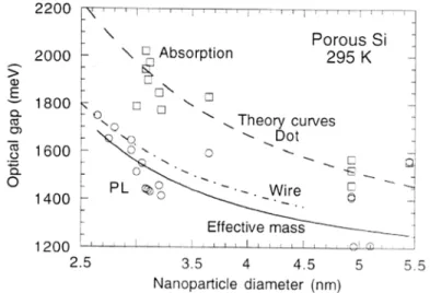
The most widely studied PL is in the far-red to orange-yellow region, which we shall denote simply as the “red” PL. This PL shifts to shorter wavelength with increasing chemical dissolution time. It was soon found that much smaller immersion times were required to produce noticeable blue shifts when the chemical dissolution was carried out in the presence of light. The spectra also show a blue shift with increasing anodization current density. The porosity of π-Si increases with increasing anodization current density. Therefore, the behavior of the red PL spectra qualitatively reflects the differences in sample porosity and hence in the dimensions of Si nanocrystallites within π-Si. The blue shift of the PL and optical absorption with increasing porosity provided the first important evidence that quantum confinement plays a significant role in π-Si, which has since been confirmed by the observation of the splitting of the luminescent states, the polarization of the PL, and the phonon replicas seen in the PL under resonant excitation (49). Nevertheless, after much research, the controversy over the origin(s) of the red PL in π-Si has persisted. This is because the PL peak wavelength and intensity are sensitive to the surface chemistry of π-Si, particularly with regard to the relative amounts of hydrogen and oxygen on the surface. Thus, besides the quantum confinement mechanism, various surface state and defect models have been invoked to explain the various results (17,49). Although direct evidence of quantum confinement effects in π-Si has been obtained via optical absorption measurements (50,51) the problems in explaining the PL of some samples in such a way are amply demonstrated by a study of oxidized π-Si samples (52). In this case the samples had a sphere-like morphology (spherites) and the optical gap was seen to be in good agreement with theoretical predictions for quantum dots, but there was a substantial energy difference between the absorption and emission data at small spherite diameters (see Fig. 1). This energy difference has since been described as being due to an oxygen passivation effect (53). For H-passivated Si, recombination is via free exciton states for all crystallite sizes and follows the expected quantum confinement behavior. For oxygen-passivated nanocrystals, a stabilized
electronic surface state is postulated to form on a Si=O covalent bond and three different recombination mechanisms can be invoked depending on the crystallite size. For larger sizes, recombination occurs via free excitons since the band gap is not wide enough to stabilize the Si=O surface state; for intermediate sizes, recombination involves a trapped electron localized on the Si atom of the Si=O bond and a free hole; and for smaller sizes, recombination is via electrons trapped on the Si=O bond. Thus the respective roles of quantum confinement and surface passivation in red light emission from π-Si are now understood and the controversy has been resolved.
Figure 1. The PL peak energy (open circles) and energy gap from optical absorption (open squares) as a function of average spherite diameter in oxidized π-Si samples at room temperature. Theoretical curves are shown for different models based on quantum dots (dashed line) and quantum wires (dot-dashed line), and in the effective mass approximation (solid line). (After Ref. 52)
Oxidation of the π-Si surface has been shown to produce blue PL (17). The blue PL is quite weak in as-prepared π-Si and becomes intense only after strong oxidation. The blue PL has a much faster decay than the red PL and its origin is still of some debate. Models under consideration include band-to-band recombination in Si nanocrystals, emission from oxide, and emission due to surface states. Blue PL has been observed also in oxide-free π-Si simply by decreasing the size of the Si crystallites in accordance with the quantum confinement mechanism (53,54). In fact, the PL can be tuned from the c-Si band gap of 1.1 eV all the way up to ~3 eV by a judicious choice of the porosity in unoxidized π-Si (53-55).
The near-infrared PL (17) at ~0.8 eV (below the bulk Si band gap) exhibits complex non-exponential dynamics, with a wide distribution of decay times, and has been assigned to deep level transitions associated with dangling bonds on the surface of the Si nanocrystallites (56).
From these considerations it is apparent that PL in π-Si is very sensitive to the chemistry of π-Si production and treatment. Crystalline-Si wires, c-Si spherites, and amorphous Si (a-Si) material, or any combination of them, may be formed in a given sample. The π-Si layers thus formed may be far from uniform, which adds to the difficulties in analyzing their optical properties. Other light emitting species may also be formed on the surfaces of the anodized and otherwise chemically treated Si.
Despite all these disadvantages, the ease of production of π-Si and the facts that the room temperature PL is very efficient [1–10% external quantum efficiency (28,48)] and that it is tunable through blue to near infrared wavelengths have led to impressive efforts to produce practical room-temperature devices. The latest red LEDs have exhibited external quantum efficiencies greater than 0.1%, lifetimes of the order of years, and extremely stable output power after appropriate passivation by alkenes (46,48,57,58). π-Si LEDs have been integrated into π-Si microelectronic circuits to provide an addressable LED display (59) and a focused-ion-beam (FIB) patterning technology has been developed (60) that permits a π-Si display technology with pixel sizes down to 100 nm. However, improvements in efficiency and power dissipation are necessary for display applications, while an increased modulation frequency is required for optical interconnects (61). One way to improve the EL efficiency, to narrow the band width, to improve the directionality, and to increase the long-term stability is to insert the LED into a π-Si resonant cavity (62). Even so, the long switching times observed in present π-Si LEDs will likely prove to be an Achilles’ heel in optoelectronic applications.
The nonlinear optical properties of π-Si may also prove useful for devices. Second harmonic generation has been observed from π-Si with a magnitude two orders greater than that from c-Si owing to the large surface-to-volume ratio of π-Si (63). A large optically induced absorption change has been observed in π-Si (64). This phenomenon has been used to form all-optical logic gates in π-Si and raises the possibility of fabricating all-optical integrated circuits on Si (43,64,65).
Silicon Nanocrystals
Rather than produce nanometer-size Si crystals by etching, as in π-Si, there have been numerous attempts at growing them either directly from a gas phase or indirectly by recrystallization within a matrix (14,26,66-68). In fact, the observation of a nanoparticle-size dependence of the PL energy in very small Si crystals passivated with hydrogen (69) predates the similar finding in π-Si (25). Takagi et al. (69) found that the PL peak energy varied as 1/d2 (3 < d < 5 nm), where d is the Si nanocrystal diameter, in accordance with quantum confinement effects predicted by a simple effective mass model. As for π-Si, however, the emitted light energy generally falls below that expected from calculations of the energy gap for Si spheres (17). Also, the confinement effect is seen (69-71) or not seen (72) in emission depending on sample preparation. Interpretation of the nanocrystal PL spectra suffers from the same ambiguities as π-Si, i.e., nanocrystal size distribution effects and surface chemistry effects (68). In addition, the nanocrystal structure may deviate from the cubic diamond structure for very small Si nanoclusters (14). Calculations (73,74) have shown that luminescence in Si nanocrystals can be due to excitons trapped at the surface, which is passivated by hydrogen or silicon oxide, while the optical absorption is characteristic of quantum confinement effects. In definitive experiments (75), the indirect nature of the Si band gap has been seen from phonon-assisted PL and absorption spectra for small (1–2 nm in diameter) surface-oxidized nanocrystals. The red PL quantum efficiency and lifetime is similar to that found for π-Si (75) indicating a similar light emission mechanism involving quantum-confined nanocrystal states. The observation of phonon assisted optical transitions in oxidized Si nanocrystals has also been reported by Kovalev et al. (76) and they found that for confinement energies above 0.7 eV the radiative transitions are governed by no-phonon quasidirect processes. Direct measurements of the conduction and valence band edges of Si nanocrystals with diameters from 1 to 5 nm using x-ray absorption and photoemission
spectra have confirmed the quantum size effect in the band structure (77). However, the increase of the band gap with decreasing nanocrystal size is lower overall than that predicted by theory. Thus, the vagaries and complexities of the nanocrystal-interface-surface system are difficult to unravel. Nevertheless, further developments of the Si-nanocrystal/SiO2-matrix system have resulted in the observation of optical gain in such structures (78), although no laser action has yet been reported.
Interesting results have come from a PL study of individual oxidized Si nanocrystals imaged in the far field using a laser scanning confocal microscope (79). Mason et al. observed a distribution of emission wavelengths, vibronic structure, and, notably, luminescence intermittency and irreversible photo-bleaching. The blinking nature of the PL from individual nanocrystals indicates a strong coupling between excitons and the surface of the quantum-dot-like nanocrystal. The phonon-assisted PL structure exhibits a much larger splitting than that found in c-Si and is ascribed to Si-O-Si vibrational stretching modes associated with the oxide passivating layer on the nanocrystal. Thus in this system the PL is mediated by the surface of the Si nanocrystal: excitons are confined near the surface and emission from these excitons is strongly coupled to vibrations in the surface passivating layer. The results imply that controlled modification of the surface by species other than oxygen should produce large differences in the PL yield. An unexpected verification of this idea has come from a totally unrelated development: the observation of intense blue PL at room temperature from Si nanocrystals formed within an a-Si matrix (80). The PL energy exhibits a size dependence and has a short lifetime (~500 ps), which is attributed to a novel quantum size effect resulting from the generation of resonant electronic states (81) in the Si nanocrystals.
Nanocrystals of Si trapped in some matrix form an attractive system for device fabrication when compared with π-Si, because of the increased surface stability and material rigidity. Visible EL has been observed, for example, from Si nanocrystals embedded in films of a-Si:H (82) and from an electrochemically-formed nanocrystalline Si thin film deposited on SnO2 (83). In the latter case the p-i-n LED at room temperature emitted orange-red light (1.8 eV) that was readily visible to the eye. The light emission is ascribed variously to near surface states (84) and the quantum size effect (83). Also, infrared emission near 1.1 eV has been obtained from a room-temperature EL device comprised of Si nanocrystals embedded within a Si-rich SiO2-x matrix (84). The PL from this structure has an external quantum efficiency of 10-3. Substantial progress in the development of such nanocrystalline-Si EL structures can be expected in future.
Quantum Wells, Wires, and Dots
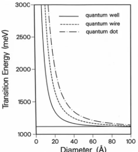
One of the major problems involved in π-Si and Si-nanocluster research and development work is the inhomogeneity of the material. Such inhomogenous broadening effects in the PL and EL can be minimized by preparing uniform Si structures in the form of quantum wells, wires, or dots. Such structures can readily be produced directly by modern epitaxial growth techniques such as planar epitaxy, quantum wire formation along wafer steps, and dot self assembly, or indirectly by etching appropriate planar structures in the case of wires and dots. The predicted Si transition energies (85,86) due to the different degrees of quantum confinement show that appreciable confinement effects are seen only for diameters less than 3 nm (see Fig. 2). Apart from π-Si, etched structures of this size have been difficult to produce in Si until recently.
Figure 2. Enlargement of the energy gap in Si quantum wells, wires, and dots according to effective mass theory. (After Ref. 85)
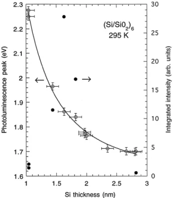
The simplest approach is to grow thin quantum wells of Si separated by wide band gap barriers. Suitable barrier candidates are SiO2, CaF2, and Al2O3 (87) and SiO2 has the additional advantage of being an excellent passivator of Si (88). Although a number of Si/barrier superlattices have been produced in the past (89) none has produced convincing evidence for quantum confinement induced emission until 1995. In that year, Lu et al. (90) reported visible light emission at room temperature from ultrathin-layer Si/SiO2 superlattices grown by molecular beam epitaxy (MBE) that exhibited a clear quantum confinement shift with Si layer thickness. According to effective mass theory and assuming infinite potential barriers, which is a reasonable approximation since wide-gap (9 eV) 1-nm-thick SiO2 barriers are used, the energy gap E for one-dimensionally confined Si should vary as
⎟⎟ ⎠ ⎞ ⎜⎜ ⎝ ⎛ + + = 2 * * 2 1 1 2 e h g m m d E E π= , [1]
where Eg is the bulk material band gap and me* and mh* are the electron and hole effective
masses (91). This simple model is a reasonable first approximation to compare with experiment for quantum wells (86). As can be seen in Fig. 3, the shift in PL peak energy with Si well thickness d is well represented by Eq. [1], with
(
)
1.60 0.72 −2+
= d
eV
E . The
very thin layers of Si (1 < d < 3 nm) have a disordered, but nearly crystalline, structure owing to the growth conditions and the huge strain at the Si–SiO2 interfaces (92). However, by reducing considerably the SiO2 thickness, epitaxial growth of the Si layers can be achieved (93). The fitted Eg of 1.60 eV is larger than that expected for c-Si (1.12
eV at 295 K), but is in excellent agreement with that of bulk a-Si (1.5–1.6 eV at 295 K). The indications of direct band-to-band recombination were confirmed by measurements via x-ray techniques of the conduction and valence band shifts with layer thickness (90,94). The fitted confinement parameter of 0.72 eV/nm2 indicates me* ≈ mh* ≈ 1,
comparable to the effective masses of c-Si at room temperature (87) The integrated intensity at first rises sharply with decreasing Si thickness until d ≈ 1.5 nm and then decreases again, which is consistent with quantum well exciton emission (95,96). The PL intensity is enhanced by factors of up to 100 on annealing and is also selectively enhanced and band-width narrowed by incorporation into an optical microcavity (97). In
a higher quality cavity, a very sharp (17 meV full width at half maximum) PL peak has been observed (98).
Figure 3. The PL peak energy (open circles) and integrated intensity (full circles) at room temperature in d-Si/a-SiO2 superlattices as a function of Si layer thickness. The solid line is the fit to the peak energy by effective mass theory (Eq. [1]). (After Ref. 91)
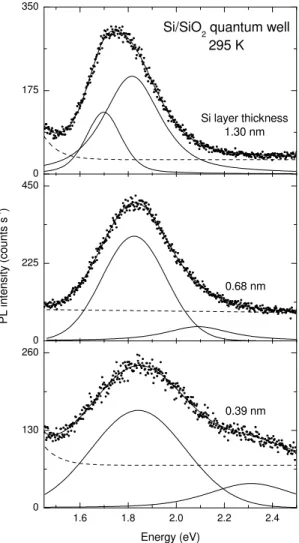
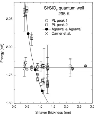
More recently, PL has been observed from c-Si quantum wells (99-103). Ultrathin single quantum wells of crystalline silicon (c-Si) confined by SiO2 were prepared by chemical processing of commercial silicon-on-insulator wafers. The PL produced by these nanometer-thick single wells comprised two bands, as shown in Fig. 4: One exhibited a fixed energy (1.8 eV), while the second increased rapidly in peak energy with decreasing c-Si layer thickness (101,102). Comparison with theories based on self-consistent (104) and first-principles calculations (105) shows that the increase in PL peak energy is consistent with that predicted for the c-Si energy gap of such wells (see Fig. 5) and it also agrees with the measured band gap variation with quantum well thickness (106). The 1.8 eV PL band is attributed to recombination of electron-hole pairs confined at the c-Si/SiO2 interface (102).
Subsequent work by Cho et al. (107) has confirmed the observation of quantum confinement induced PL from c-Si/SiO2 wells produced by high temperature thermal oxidation of ELTRAN SOI wafers, but in this case weak or no interface mediated PL was seen.
Room temperature PL at visible wavelengths has also been observed from MBE-grown nanocrystalline Si/CaF2 superlattices (89), but in this case the luminescence is related to localized states located well below the Si layer optical absorption edge (108). Nevertheless, these states do exhibit some sensitivity to confinement effects. Likewise, the visible PL observed in Si/SiNx superlattices grown by MBE in association with an electron-cyclotron-resonance plasma surface treatment (109) exhibited only a weak
dependence on quantum well confinement compared with Si/SiO2. Further evidence of confinement-induced PL in plasma-enhanced chemical vapor deposition (PECVD)-grown Si/SiNx single quantum well structures has been obtained by Steigmeier et al. (110). 1.6 1.8 2.0 2.2 2.4 0 130 260 0.39 nm Energy (eV) 0 225 450 0.68 nm P L i n tens it y (c ou nts s -1 ) 0 175 350 Si/SiO 2 quantum well 295 K Si layer thickness 1.30 nm
Figure 4. Room temperature PL from single c-Si/a-SiO2 quantum wells of different thickness. The PL line shape has been fitted with the two bands (indicated by the solid line passing through the data points) shown below by the solid lines. The dashed line is the fitted background. (After Ref. 101)
Theoretical calculations of the optical properties of Si/SiO2 superlattices based on an empirical pseudopotential homojunction model (111) revealed that for Si layers in the (100) direction the energy gap is pseudodirect, i.e., the optical transition matrix element is smaller than that of a direct transition as in bulk GaAs. Nevertheless, the energy increases with decreasing Si quantum-well thickness and the transition matrix element increases steeply up to ~2 nm thickness and then decreases again in general agreement with the experimental results. Tight binding bandstructure calculations for Sim/(SiO2)n
crystalline superlattices with the number of unit cells m,n ≤ 5 show a striking new feature (112). Besides the expected increase in the band gap due to quantum confinement, the confined bands along the Γ–Z symmetry direction are essentially dispersionless and exhibit a strongly-nested direct band gap character at the minimum energy gap of the
system. Thus, these superlattices produce a high radiative efficiency for a 1–3 nm (m = 2–5) Si layer thickness (112), as found experimentally (100-102). The self-consistent electronic structures of Si/CaF2 superlattices have been calculated by means of the linear muffin-tin orbital method in the atomic-sphere approximation (113). These calculations could not explain the experimental difference between absorption and PL in such superlattices (see Ref. 108 and references therein), but they did emphasize that both quantum confinement and adequate passivation of the Si layers are necessary in order to observe visible wavelength PL.
0.0 0.5 1.0 1.5 2.0 2.5 3.0 1.50
1.75 2.00 2.25
Si/SiO2 quantum well 295 K
PL peak 1 PL peak 2 Agrawal & Agrawal Carrier et al. E n er gy ( e V ) Si layer thickness (nm)
Figure 5. Experimental results (○,□) for the energies of the two PL bands of single c-Si/a-SiO2 quantum wells as a function of well thickness compared with the theory of Agrawal and Agrawal (●) (104) and Carrier et al. (×) (105). The solid line is an interpolation of the theoretical data. The error bars represent the standard deviation in the peak energy determined from the fits. The horizontal solid line is a least-squares fit to the data of peak number 1. (After Ref. 102)
The PL obtained from as-grown and annealed Si/SiO2 superlattices offers interesting prospects for the fabrication of a Si-based light emitter that can be tuned from the blue to the near infrared by varying the Si layer thickness and/or the annealing conditions, all using available vacuum deposition technology and standard Si wafer processing techniques. The luminescence can be very bright indeed due to a high quantum efficiency resulting from strong confinement of carriers and nearly perfect Si/SiO2 interfaces especially in annealed samples, which reduces competing defect-induced interface recombination. The next important step is to develop LEDs based on such superlattices. Several prototype devices have been constructed in Si/SiO2 (114-119) and Si/CaF2 (120) and all report visible EL, although as yet there is no strong evidence in many cases that the emission originates from confined states in the Si quantum wells. The EL from the Si/SiO2 superlattices is notably stable (114,115). An optically pumped light emitting device is certainly possible, but an electrically excited LED requires vertical carrier
transport through the wide band gap a-SiO2 barriers. Fortunately, for thin enough barriers such transport via hole tunneling has been observed (121,122). Remarkably, a silicon light-emitting transistor for on-chip optical interconnection has been produced (123). Following a theoretical prediction of a large optical gain in ultra thin silicon quantum wells (124), Saito et al. (125) have recently observed optical gain and stimulated emission by current injection into an ultra thin layer of silicon embedded in a resonant optical cavity. Thus the production of a laser based on such structures is now a real possibility.
Quantum wires obtained by etching Si/Si1-xGex heterostructures have been investigated by several groups (see, for example, Refs. 126 and 127). In PL measurements, wires defined by electron beam lithography and reactive ion etching have shown small blue shifts of up to 30 meV in the Si1-xGex alloy peak at ~1.1 eV due to a combination of strain and confinement (126,127). Alternatively, Si1-xGex wires have been grown on V groove patterned Si substrates (128): The infrared emission (PL and EL) in this case exhibits a large optical anisotropy (129). No significant intensity enhancements compared with PL from quantum well transitions have been realized in these wire structures.
Until recently, it has not been possible to produce thin enough freestanding wires of c-Si by etching techniques to observe quantum confinement effects, although room temperature PL at wavelengths from 400–850 nm is found for pillars with diameters ~10 nm (see, for example, Refs. 130-132 and references therein). Recently, an EL device based on such Si nanopillars has been produced: The device emitted red light that was visible to the naked eye (133). New etching techniques have now been developed for fabricating Si quantum wires with dimensions in the sub-10-nm region that after thermal oxidation should allow investigation of the optical properties of sub-2-nm wires in conventional wire (134) and free-standing pillar (135) form. The direct growth of free standing Si nanowires by various vapor transport methods is now being explored (see Ref. 136 and references therein).
Theoretical calculations of the electronic structure and optical properties of H passivated Si quantum wires have been reported by a number of research groups (see, for example, Ref. 137 and references therein). First principles calculations show the same band nesting phenomenon and near-flat dispersion along the Γ–Z symmetry (wire) direction, as described above for Si quantum wells, and the occurrence of direct gaps (137,138).
Attention has now turned mainly to the production of Si1-xGex quantum dots (139), as these produce the strongest confinement effects for a given diameter or can achieve desired confinements with smaller diameters than for wires. A number of first principles calculations have been performed for H-passivated Si quantum dots (see Ref. 140 and references therein) and they all show a steep increase in the optical gap energy with decreasing dot size below 3–5 nm. Quantum dots fabricated by etching Si/ Si1-xGex superlattices have produced 4-K PL at 0.97 eV that is 200 times brighter in 60 nm dots compared with the unetched superlattice PL (141). Similar studies of Si1-xGex dots fabricated by self-assembling island growth on Si have shown an increased luminescence efficiency due to the localization of excitons in the dots (142). In the latter case, the dots were buried in Si, which has the advantage of minimizing surface defect recombination. In both cases, EL has been observed from diode structures at low temperatures (142,143) and at room temperature (143). The infrared EL at 4.2 K in the dot is two orders of magnitude higher in intensity than in the as-grown superlattice. At room temperature, the dot EL at 1.3 µm is only 50% less efficient, with a threshold injection current of ~0.1
pA/dot and an electrical input to optical output power conversion efficiency of 0.14% (143).
In subsequent work on Si quantum dots ~10 nm in size formed in a-Si/SiO2 superlattices by controlled crystallization, Tsybeskov et al. (144) have shown that the PL emitted near 1.1 eV is remarkably efficient (~0.2% external quantum efficiency at 300 K) compared with c-Si. The observation of sharp structure in the superlattice PL spectrum proves that the Si dots are extremely pure, primarily as a result of self-purification during thermal crystallization (144). The high room temperature quantum efficiency indicates that strong luminescence in indirect gap semiconductor dots does not necessarily require strong quantum confinement, but can arise simply from spatial confinement in well passivated nanocrystals. Finally, a shift of the PL peak toward higher energies was found with smaller-size (< 10 nm) Si dots. The PL in such dots can be tuned up in energy by confinement and down in energy by alloying of Ge with Si. The latter case has been investigated in MBE-grown Si0.5Ge0.5 dots in a coherent wave superlattice structure. Here, strong no-phonon PL was obtained at ~0.8 eV (1.55 µm) that could easily be varied in wavelength by changing the Ge content (1,145). The SiGe dot electron-hole recombination can not only be efficient but also very fast (see Ref. 146 for a review).
It is quite conceivable that this diverse work on Si quantum dots could lead to a new generation of Si/Si1-xGex optoelectronic devices at the optical fiber communication wavelengths of 1.3 and 1.55 µm.
Prospects for Silicon Based Optoelectronic Devices
Although a considerable number of optical detectors and waveguide structures have been created from Si-based materials (5,8-10,147.148) there is still a paucity of LEDs constructed from Si and, most importantly for many all-Si optoelectronic applications, no lasers [apart from optically-pumped Si Raman lasers (9)]. The requirements for an acceptable semiconductor laser for optical fiber applications are rather stringent: 5–10 mW of laser facet power at 1.3 or 1.55 µm, maximum laser threshold less than 70 mA, spectral width less than 10 nm, operation over the temperature range -40°C to +85°C, average lifetime of 106 hr, and low cost (147).
Of the materials systems considered here, LEDs made from Si:Er show the most immediate promise for device applications at 1.54 µm. An optoelectronic device has been constructed (1,9) comprising an edge emitting Si:Er LED integrated with a Si waveguide on a SOI substrate. The EL linewidth of such LEDs at room temperature is approximately 10 nm (136). This narrow linewidth and the fixed emission wavelength augers well for optical fiber communication systems with high bandwidth capacity. Optical gain at 1.54 µm has been obtained in suitable Si waveguide structures (137) and laser emission could follow if the room temperature quantum efficiency can be improved sufficiently, although this seems now to be unlikely.
Porous Si LEDs emitting at orange-red wavelengths are no longer just a curiosity with the announcement of LEDs having reasonable external quantum efficiencies (0.1%), lifetimes of the order of years (58) and low driving voltages (2–5 V) in forward bias (151), and also of devices with integrated Si transistor drivers (59). Apart from display applications (59), however, the long lifetime and broad linewidth of the optical emission will limit optical communications applications of π-Si LEDs, and it is not clear whether current injection lasers will ever be made from π-Si. The need to be compatible with existing large-scale Si processing also leads to difficulties with electrochemically created π-Si. It is likely that oxidized Si nanoparticles will eventually prove to be superior to π-Si
in this regard and also in device stability, but the long lifetime and wide band width of the emitted light are still going to limit device performance. Nevertheless, π-Si is a versatile material and offers extremely diverse optoelectronic functionality to Si in the areas of infrared and visible waveguiding, photodetection, and photomodulation (152).
Light emission from quantum well and dot structures may yet hold the most promise for producing lasers at wavelengths across the visible into the infrared. The Si/SiO2 multiple (89) and single quantum well structures are well suited for visible and near-infrared wavelength lasers at room temperature. Their optical absorption characteristics are ideal for optical pumping in a planar microcavity and their electrical characteristics are amenable to injection laser design. With the recent observation of stimulated emission by Saito et al. (125), this system holds the most promise at present for room temperature laser action. Quantum dot LEDs made from Si/Si1-xGex (143,146) show considerable potential for laser applications at 1.3 and possibly 1.55 µm. However, much more research and development work on these structures is required before this potential can be realized.
In conclusion, considerable progress has been made over the last decade on obtaining efficient light emission from a wide variety of Si-based materials. This work has led to the development of light emitting devices that are just now reaching useful performance levels. The intensity of research and development on light emission in Si is increasing as a result of these stimulating advances in materials engineering and technology. It is likely that a Si-based injection laser will emerge from this research in the near future, although the actual active laser material could be none of those discussed here, because of the burgeoning diversification (7,9,10,106,121,146,153-158) in Si-based materials and their applications.
Acknowledgments
The work carried out at the National Research Council of Canada has only been possible because of continued support from the Institute for Microstructural Sciences (IMS). My grateful thanks to all those within and outside IMS who have contributed to these studies, and particularly to J.-M. Baribeau and Z.-H. Lu.
References
1. D.J. Lockwood, in Silicon-Based Materials and Devices, edited by H.S. Nalwa (Academic Press, San Diego, 2001), p. 225.
2. E. Kasper and F. Schäffler, in Strained-Layer Superlattices: Materials Science
and Technology, edited by T.P. Pearsall (Academic Press, Boston, 1991), p. 223. 3. G. Abstreiter, Physics World 5 (3), 36 (1992).
4. B.A. Saleh and M.C. Teich, Fundamentals of Photonics (Wiley, New York, 1991).
5. R.A. Soref, Proc. IEEE 81, 1687 (1993).
6. E. Kasper and H. Presting, SPIE Proc. 1361, 302 (1990). 7. R.A. Soref, J. Vac. Sci. Technol. A 14, 913 (1996). 8. R. Soref, MRS Bulletin 23 (4), 20 (1998).
9. L. Pavesi and D.J. Lockwood, Silicon Photonics (Springer, Berlin, 2004). 10. R. Soref, IEEE J. Sel. Top. Quantum Electronics, 12, 1678 (2006). 11. S.S. Iyer and Y.-H. Xie, Science 260, 40 (1993).
13. D.J. Lockwood, Light Emission in Silicon: From Physics to Devices (Academic Press, San Diego, 1997).
14. L.C. Kimerling, K.D. Kolenbrander, J. Michel, and J. Palm, Solid State Phys. 50, 333 (1997).
15. R.W. Collins, P.M. Fauchet, I. Shimizu, J.-C. Vial, T. Shimada, and
A.P. Alivisatos, Advances in Microcrystalline and Nanocrystalline
Semiconductors—1996 (Materials Research Society, Pittsburgh, 1997).
16. L.T. Canham, M.J. Sailor, K. Tanaka, and C.-C. Tsai, Microcrystalline and
Nanocrystalline Semiconductors—1998 (Materials Research Society, Pittsburgh, 1999).
17. D.J. Lockwood, Solid State Commun. 92, 101 (1994). 18. Properties of Silicon (INSPEC, London, 1988).
19. J.R. Chelikowsky and M.L. Cohen, Phys. Rev. B 14, 556 (1976).
20. J.I. Pankove, Optical Processes in Semiconductors (Dover, New York, 1971). 21. J.R. Haynes and H.B. Briggs, Phys. Rev. 86, 647 (1952).
22. P.J. Dean, Luminescence of Inorganic Solids (Academic Press, New York, 1966), Chapter 3.
23. R. Newan, Phys. Rev. 100, 700 (1955).
24. P.A. Wolf, J. Phys. Chem. Solids 16, 184 (1960).
25. A.T. Obeidat, Z. Kalayjian, A.G. Andreou, and J.B. Khurgin, Appl. Phys. Lett.
70, 470 (1997).
26. A.D Yoffe, Advan. Phys. 42, 173 (1993).
27. L.T. Canham, Appl. Phys. Lett. 57, 1046 (1990).
28. A.G. Cullis, L.T. Canham, and P.D.J. Calcott, J. Appl. Phys. 82, 909 (1997). 29. L. Brus, Appl. Phys. A 53, 465 (1991).
30. A. Uhlir, Jr., Bell Syst. Tech. J. 35, 333 (1956).
31. A.G. Cullis, and L.T. Canham, Nature 353, 335 (1991). 32. V. Lehmann and U. Gösele, Appl. Phys. Lett. 58, 856 (1991).
33. A. Bsiesy, J.C. Vial, F. Gaspard, R. Herino, M. Ligeon, F. Muller, R. Romestain, A. Wasiela, A. Halmaoui, and G. Bomchil, Surf. Sci. 254, 195 (1991).
34. N. Koshida and H. Koyama, Jpn. J. Appl. Phys. 30, L1221 (1991).
35. S. Gardelis, J.S. Rimmer, P. Dawson, B. Hamilton, R.A. Kubiak, T.E. Whall, and E.H.C. Parker, Appl. Phys. Lett. 59, 2118 (1991).
36. A. Halimaoui, C. Oules, G. Bomchil, A. Bsiesy, F. Gaspard, R. Herino, M. Ligeon, and F. Muller, Appl. Phys. Lett. 59, 304 (1991).
37. A. Richter, P. Steiner, F. Kozlowski, and W. Lang, IEEE Electron Device Lett.
12, 691 (1991).
38. N. Koshida and H. Koyama, Appl. Phys. Lett. 60, 347 (1992).
39. D.C. Bensahel, L.T. Canham, and S. Osscicini, Optical Properties of Low
Dimensional Structures (Kluwer, Dordrecht, 1993).
40. P.M. Fauchet, C.C. Tsai, L.T. Canham, I. Shimizu, and Y. Aoyagi,
Microcrystalline Semiconductors: Materials Science and Devices (Materials Research Society, Pittsburgh, 1993).
41. Z.C. Feng and R. Tsu, Porous Silicon (World Scientific, Singapore, 1994). 42. B. Hamilton, Semicond. Sci. Technol. 10, 1187 (1995).
43. Y. Kanemitsu, Phys. Reports 263, 1 (1995).
44. J.C. Vial and J. Derrien, Porous Silicon Science and Technology (Springer-Verlag, Berlin, 1995).
45. R. Hérino and W. Lang, Porous Silicon and Related Materials (Elsevier, Amsterdam, 1995).
46. D.J. Lockwood, P.M. Fauchet, N. Koshida, and S.R.J. Brueck, Advanced
Luminescent Materials (The Electrochemical Society, Pennington, NJ, 1996). 47. P.M. Fauchet, J. Lumin. 70, 294 (1996).
48. P.M. Fauchet, in Light Emission in Silicon, edited by D.J. Lockwood (Academic Press, San Diego, 1997), Chapter 6.
49. P.D.J. Calcott, Mat. Sci. Eng. B 51, 132 (1998).
50. I. Sagnes, A. Halimaoui, G. Vincent, and P.A. Badoz, Appl. Phys. Lett. 62, 1155 (1993).
51. D.J. Lockwood, A. Wang, and B. Bryskiewicz, Solid State Commun. 89, 587 (1994).
52. D.J. Lockwood, and A.G. Wang, in Photoluminescence in Porous Silicon Due
to Quantum Confinement, edited by D.J. Lockwood, P.M. Fauchet, N. Koshida, and S.R.J. Brueck (The Electrochemical Society, Pennington, NJ, 1996), p. 166. 53. M.V. Wolkin, J. Jorne, P.M. Fauchet, G. Allan, and C. Delarue, Phys. Rev. Lett.
82, 197 (1999).
54. H. Mizuno, H. Koyama, and N. Koshida, Appl. Phys. Lett. 69, 3779 (1996). 55. G. Polisski, H. Heckler, D. Kovalev, M. Schwartzkoff, and F. Koch, Appl. Phys.
Lett. 73, 1107 (1998).
56. F. Koch, Mater. Res. Soc. Symp. Proc. 298, 319 (1993).
57. B. Gelloz, T. Nakagawa, and N. Koshida, Appl. Phys. Lett. 73, 2021 (1998). 58. B. Gelloz, H. Sano, R. Boukherroub, D.D.M. Wayner, D.J. Lockwood and N.
Koshida, Appl. Phys. Lett. 83, 2342 (2003).
59. K.D. Hirschman, L. Tsybeskov, S.P. Duttagupta, and P.M. Fauchet, Nature 384, 338 (1996).
60. P. Schmuki, L.E. Erickson, and D.J. Lockwood, Phys. Rev. Lett. 80, 4060 (1998).
61. L. Tsybeskov, S.P. Duttagupta, K.D. Hirschman, and P.M. Fauchet, Appl. Phys.
Lett. 68, 2058 (1996).
62. L. Pavesi, R. Guardini, and C. Mazzoleni, Solid State Commun. 97, 1051 (1996). 63. K.-Y. Lo and J.T. Lue, IEEE Photon. Technol. Lett. 5, 651 (1993).
64. T. Matsumoto, N. Hasegawa, T. Tamaki, K. Ueda, T. Futagi, H. Mimura, and Y. Kanemitsu, Jpn. J. Appl. Phys. 33, L35 (1994).
65. T. Matsumoto, M. Daimon, H. Mimura, Y. Kanemitsu, and N. Koshida,
J. Electrochem. Soc. 142, 3528 (1995).
66. H. Kamimura, Light Emission from Novel Silicon Materials, Supplement B to J. Phys. Soc. Japan, Vol. 63 (Physical Society of Japan, Tokyo, 1994).
67. T. Ogawa and Y. Kanemitsu, Optical Properties of Low-Dimensional Materials (World Scientific, Singapore, 1995).
68. Y. Kanemitsu, in Light Emission in Silicon, edited by D.J. Lockwood (Academic Press, San Diego, 1997), Chapter 5.
69. H. Takagi, H. Ogawa, Y. Yamazaki, A. Ishizaki, and T. Nakagiri, Appl. Phys.
Lett. 56, 2379 (1990).
70. S. Schuppler, S.L. Friedman, M.A. Marcus, D.L. Adler, Y.-H. Xie, F.M. Ross, T.D. Harris, W.L. Brown, Y.J. Chabal, L.E. Brus, and P.H. Citrin, Phys. Rev.
Lett. 72, 2648 (1994).
71. Y. Kanzawa, T. Kageyama, S. Takeoka, M. Fujii, S. Hayashi, and K. Yamamoto, Solid State Commun. 102, 533 (1997).
72. Y. Kanemitsu, T. Ogawa, K. Shiraishi, and K. Takeda, Phys. Rev. B 48, 4883 (1993).
73. G. Allan, C. Delerue, and M. Lannoo, Phys. Rev. Lett. 76, 2961 (1996).
74. C. Delerue, G. Allan, and M. Lannoo, in Light Emission in Silicon, edited by D.J. Lockwood (Academic Press, San Diego, 1997), Chapter 7.
75. L.E. Brus, P.F. Szajowski, W.L. Wilson, T.D. Harris, S. Schuppler, and P.H. Citrin, J. Amer. Chem. Soc. 117, 2915 (1995).
76. D. Kovalev, H. Heckler, M. Ben-Chorin, G. Polisski, M. Schwartzkopff, and F. Koch, Phys. Rev. Lett. 81, 2803 (1998).
77. T. van Buuren, L.N. Dinh, L.L. Chase, W.J. Siekhaus, and L.J. Terminello,
Phys. Rev. Lett. 80, 3803 (1998).
78. L. Pavesi, L. Dal Negro, C. Mazzoleni, G. Franzo, and F. Priolo, Nature 408, 440 (2000).
79. M.D. Mason, G.M. Credo, K.D. Weston, and S.K. Buratto, Phys. Rev. Lett. 80, 5405 (1998).
80. X. Zhao, S. Komuro, S. Fujita, H. Isshiki, Y. Aoyagi, and T. Sugano, Mat. Sci.
Eng. B 51, 154 (1998).
81. S. Nomura, T. Iitaka, X. Zhao, T. Sugano, and Y. Aoyagi, Mat. Sci. Eng. B 51, 146 (1998).
82. S. Tong, X.-N. Liu, L.-C. Wang, F. Yan, and X.-M. Bao, Appl. Phys. Lett. 69, 596 (1996).
83. T. Toyama, T. Matsui, Y. Kurokawa, H. Okamoto, and Y. Hamakawa, Appl.
Phys. Lett. 69, 1261 (1996).
84. L. Tsybeskov, K.L. Moore, D.G. Hall, and P.M. Fauchet, Phys. Rev. B 54, R8361 (1996).
85. D.J. Lockwood, G.C. Aers, L.B. Allard, B. Bryskiewicz, S. Charbonneau, D.C. Houghton, J.P. McCaffrey, and A. Wang, Can. J. Phys. 70, 1184 (1992). 86. A. Zunger and L.-W. Wang, Appl. Surf. Sci. 102, 350 (1996).
87. R. Tsu, Nature 364, 19 (1993).
88. C.J. Frosch and L. Derick, J. Electrochem. Soc. 104, 547 (1957). 89. D.J. Lockwood, Phase Transitions 68, 151 (1999).
90. Z.H. Lu, D.J. Lockwood, and J.-M. Baribeau, Nature 378, 258 (1995).
91. D.J. Lockwood, Z.H. Lu, and J.-M. Baribeau, Phys. Rev. Lett. 76, 539 (1996). 92. Z.H. Lu, D.J. Lockwood, and J.-M. Baribeau, Solid-State Electron. 40, 197
(1996).
93. R. Tsu, A. Filios, C. Lofgren, K. Dovidenko, and C.G. Waugh, Electrochem.
Solid-State Lett. 1, 80 (1998).
94. D.J. Lockwood, J.-M. Baribeau, and Z.H. Lu, in Advanced Luminescent
Materials, edited by D.J. Lockwood, P.M. Fauchet, N. Koshida, and S.R.J. Brueck (The Electrochemical Society, Pennington, NJ, 1996), p. 339.
95. J.A. Brum and G. Bastard, J. Phys. C. Solid State Phys. 18, L789 (1985).
96. Z.H. Lu, J.-M. Baribeau, D.J. Lockwood, M. Buchanan, N. Tit, C. Dharma-wardana, and G.C. Aers, SPIE Proc. 3491, 457 (1998).
97. B.T. Sullivan, D.J. Lockwood, H.J. Labbé, and Z.-H. Lu, Appl. Phys. Lett. 69, 3149 (1996).
98. D.J. Lockwood, B.T. Sullivan, and H.J. Labbé, J. Lumin. 80, 75 (1999). 99. D.J. Lockwood, Z.H. Lu, and D. Grozea, SPIE Proc. 4808, 40 (2002).
100. D.J. Lockwood, Z.H. Lu and D. Grozea, Physics of Semiconductors 2002 (A.R. Long and J.H. Davies, Eds.), Institute of Physics, Bristol, 171, G3.1 (2003).
101. D.J. Lockwood, M.W.C. Dharma-wardana, Z.H. Lu, D.H. Grozea, P. Carrier and L.J. Lewis, Quantum Confined Semiconductor Nanostructures (V.I. Klimov, J.M. Buriak, D.D.M. Wayner, F. Priolo, B. White and L. Tsybeskov, Eds.), MRS, Pittsburgh, PA, 737, 243 (2003).
102. D.J. Lockwood, R.L. Williams and Z.-H. Lu, Nanoscale Devices, Materials,
and Biological Systems: Fundamentals and Applications (M. Cahay, M. Urquidi-Macdonald, S. Bandyopadhyay, P. Guo, H. Hasegawa, N. Koshida, J.P. Leburton, D.J. Lockwood, S. Seal and A. Stella, Eds.), Electrochem. Soc., Pennington, NJ, 243 (2005).
103. E.-C. Cho, M.A. Green, R. Corkish, P. Reece, M. Gal, and S.-H. Lee, J. Appl.
Phys. 101, 024321 (2007).
104. B. K. Agrawal and S. Agrawal, Appl. Phys. Lett. 77, 3039 (2000).
105. P. Carrier, L. J. Lewis, and M. W. C. Dharma-wardana, Phys. Rev. B 65, 165339 (2002).
106. Z.H. Lu, and D. Grozea, Appl. Phys. Lett. 80, 255 (2002).
107. E.-C. Cho, M. A. Green, R. Corkish, P. Reece, M. Gal, and S.-H. Lee, J. Appl.
Phys. 101, 063105 (2007).
108. F. Basani, S. Ménard, and F. Arnaud d’Avitaya, Phys. Stat. Sol. (a) 165, 49 (1998).
109. J.-M. Baribeau, D.J. Lockwood, Z.H. Lu, H.J. Labbé, S.J. Rolfe, and G.I. Sproule, J. Lumin. 80, 417 (1999).
110. E.F. Steigmeier, R. Morf, D. Grützmacher, H. Auderset, B. Delley, and R. Wessicken, Appl. Phys. Lett. 69, 4165 (1996).
111. J.-B. Xia and K.W. Cheah, Phys. Rev. B 56, 14925 (1997).
112. N. Tit and M.W.C. Dharma-wardana, Solid State Commun. 106, 121 (1998). 113. E. Degoli and S. Ossicini, Phys. Rev. B 57, 14776 (1998).
114. R. Tsu, Q. Zhang, and A. Filios, SPIE Proc. 3290, 246 (1997).
115. A.G. Nassiopoulou, V. Ioannou-Sougleridis, P. Photopoulos, A. Travlos, V. Tsakiri, and D. Papadimitriou, Phys. Stat. Sol. (a) 165, 79 (1998).
116. G.G. Qin, S.Y. Ma, Z.C. Ma, W.H. Zong, and L.P. You, Solid State Commun.
106, 329 (1998).
117. L. Heikkilä, T. Kuusela, H.-P. Hedman, and H. Ihantola, Appl. Surf. Sci. 133, 84 (1998).
118. S. Saito, D. Hisamoto, H. Shimizu, H. Hamamura, R. Tsuchiya, Y. Matsui, T. Mine, T. Arai, N. Sugii, K. Torri, S. Kimura and T. Onai, Jap. J. Appl. Phys. 45, L679 (2006).
119. W.K. Tan, Q. Chen, J.D. Ye, M.B. Yu, G.-Q. Lo and D.-L. Kwong, IEEE
Electron. Dev. Lett. 29, 344 (2008).
120. V. Ioannou-Sougleridis, V. Tsakiri, A.G. Nassiopoulou, P. Photopoulos, F. Bassani, and F. Arnaud d’Avitaya, Phys. Stat. Sol. (a) 165, 97 (1998).
121. L. Tsybeskov, G.F. Grom, R. Krishnan, L. Montes, P.M. Fauchet, D. Kovalev, J. Diener, V. Timoshenko, F. Koch, J.P. McCaffrey, J.-M. Baribeau, G.I. Sproule, D.J. Lockwood, Y.M. Niquet, C. Delerue and G. Allan, Europhys. Lett. 55, 552 (2001).
122. B.V. Kamenev, G.F. Grom, D.. Lockwood, J.P. McCaffrey, B. Laikhtman and L. Tsybeskov, Phys. Rev. B 69, 235306 (2004).
123. S. Saito, D. Hisamoto, H. Shimizu, H. Hamamura, R. Tsuchiya, Y. Matsui, T. Mine, T. Arai, N. Sugii, K. Torii, S. Kimura and T. Onai, Appl. Phys. Lett. 89, 163504 (2006).
124. Y. Suwa and S. Saito, Phys. Rev. B 79, 233308 (2009).
125. S. Saito, Y. Suwa, H. Arimoto, N. Sakuma, D. Hisamoto, H. Uchiyama, J. Yamamoto, T. Sakamizu, T. Mine, S. Kimura, T. Sugawara and M. Aoki, Appl.
Phys. Lett. 95, 241101 (2009).
126. Y.S. Tang, C.D.W. Wilkinson, C.M. Sotomayor Torres, D.W. Smith, T.E. Whall, and E.H.C. Parker, Solid State Commun. 85, 199 (1993).
127. J. Lee, S.H. Li, J. Singh, and P.K. Bhattacharaya, J. Electron. Mat. 23, 831 (1994).
128. N. Usami, T. Mine, S. Fukatsu, and Y. Shiraki, Appl. Phys. Lett. 63, 2789 (1993).
129. N. Usami, T. Mine, S. Fukatsu, and Y. Shiraki, Appl. Phys. Lett. 64, 1126 (1994).
130. H.I. Liu, N.I. Maluf, R.F.W. Pease, D.K. Biegelsen, N.M. Johnson, and F.A. Ponce, J. Vac. Sci. Technol. B 10, 2846 (1992).
131. A.G. Nassiopoulos, S. Grigoropoulos, and D. Papadimitriou, in Advanced
Luminescent Materials, edited by D.J. Lockwood, P.M. Fauchet, N. Koshida, and S.R.J. Brueck (The Electrochemical Society, Pennington, NJ, 1996), p. 296. 132. S.H. Zaidi, A.-S. Chu, and S.R.J. Brueck, in Advanced Luminescent Materials,
edited by D.J. Lockwood, P.M. Fauchet, N. Koshida, and S.R.J. Brueck (The Electrochemical Society, Pennington, NJ, 1996), p. 307.
133. A.G. Nassiopoulos, S. Grigoropoulos, and D. Papadimitriou, Appl. Phys. Lett.
69, 2267 (1996).
134. H. Namatsu, K. Kurihara, M. Nagase, and T. Makino, Appl. Phys. Lett. 70, 619 (1997).
135. H.I. Liu, D.K. Biegelsen, F.A. Ponce, N.M. Johnson, and R.F.W. Pease, Appl.
Phys. Lett. 64, 1363 (1994).
136. H.-Y. Chang, L. Tsybeskov, S. Sharma, T.I. Kamins, X. Wu and D.J. Lockwood,
Appl. Phys. Lett. 95, 133120 (2009).
137. F. Buda and J. Kohanoff, Prog. Quant. Electr. 18, 201 (1994).
138. S. Ossicini, C.M. Bertoni, M. Biagini, A. Lugli, G. Roma, and O. Bisi, Thin
Solid Films 297, 154 (1997).
139. J.-M. Baribeau, X. Wu, N.L. Rowell and D.J. Lockwood, J. Phys.: Condens.
Matter 18, R139 (2006).
140. F.A. Reboredo, A. Franceschetti, and A. Zunger, Phys. Rev. B 61, 13073 (2000). 141. Y.S. Tang, C.M. Sotomayor Torres, R.A. Kubiak, D.A. Smith, T.E. Whall,
E.H.C. Parker, H. Presting, and H. Kibbel, in The Physics of Semiconductors,
Vol. 2, edited by D.J. Lockwood (World Scientific, Singapore, 1995), p. 1735. 142. R. Apetz, L. Vescan, A. Hartmann, C. Dieker, and H. Lüth, Appl. Phys. Lett. 66,
445 (1995).
143. Y.S. Tang, W.-X. Ni, C.M. Sotomayor Torres, and G.V. Hansson, Electron. Lett.
31, 1385 (1995).
144. L. Tsybeskov, K.D. Hirschman, S.P. Duttagupta, M. Zacharias, P.M. Fauchet, J.P. McCaffrey, and D.J. Lockwood, Appl. Phys. Lett. 72, 43 (1998).
145. L. Tsybeskov, B.V. Kamenev, J.-M. Baribeau and D.J. Lockwood, IEEE J. Sel.
Top. Quantum Electronics, 12, 1579 (2006).
146. L. Tsybeskov and D.J. Lockwood, Proc. IEEE 97, 1284 (2009). 147. D.G. Hall, Mat. Res. Soc. Symp. Proc. 298, 367 (1993).
149. B. Zheng, J. Michel, F.Y.G. Ren, L.C. Kimerling, D.C. Jacobson, and J.M. Poate, Appl. Phys. Lett. 64, 2842 (1994).
150. X. Zhao, S. Komuro, H. Isshiki, Y. Aoyagi, and T. Sugano, Appl. Phys. Lett. 74, 120 (1999).
151. R.T. Collins, P.M. Fauchet, and M.A. Tischler, Physics Today 50 (1), 24 (1997). 152. L.T. Canham, T.I. Cox, A. Loni, and A.J. Simons, Appl. Surf. Sci. 102, 436
(1996).
153. H. Shinoda, T. Nakajima, K.Ueno and N. Koshida, Nature 400, 853 (1999). 154. G.F. Grom, D.J. Lockwood, J.P. McCaffrey, H.J. Labbé, P.M. Fauchet, B.
White Jr., J. Diener, D. Kovalev, F. Koch, and L. Tsybeskov, Nature 407, 358 (2000).
155. R Boukherroub, S. Morin, D.D.M. Wayner, F. Bensebba, G.I. Sproule, J.-M. Baribeau and D.J. Lockwood, Chem. Mater. 13, 2002 (2001).
156. R. Boukherroub, D.D.M. Wayner, G.I. Sproule, D.J. Lockwood and L.T. Canham, Nano Lett. 1, 713 (2001).
157. R. Boukherroub, D.D.M. Wayner and D.J. Lockwood, Appl. Phys. Lett. 81, 601 (2002).