Co-Optimizing Silicon Solar Cell Processing for
Efficiency and Throughput
by
Ashley E. Morishige
Bachelor of Engineering
Thayer School of Engineering at Dartmouth College (2011)
Submitted to the Department of Mechanical Engineering
in partial fulfillment of the requirements for the degree of
Master of Science in Mechanical Engineering
at the
MASSACHUSETTS INSTITUTE OF TECHNOLOGY
AM4r)VF
IMASSACHUSETTS INSTWE OF TECHNOLOGYNOV
12
2013
LIBRARIES
September 2013
@
Massachusetts Institute of Technology 2013. All rights reserved.
A u th or ... .. ...
Department of Mechanical ngineering
August 9, 2013
Certified by...
Tonio Buonassisi
Associate Professor of Mechanical Engineering
Thesis Supervisor
A ccepted by ...
David Hardt, ProfessoW'f'oi'chanical Engineering
Chairman, Department Committee on Graduate Theses
Co-Optimizing Silicon Solar Cell Processing for Efficiency
and Throughput
by
Ashley E. Morishige
Submitted to the Department of Mechanical Engineering on August 9, 2013, in partial fulfillment of the
requirements for the degree of
Master of Science in Mechanical Engineering
Abstract
Crystalline silicon solar cells are a proven renewable energy technology, but they have yet to reach low costs commensurate with subsidy-free, grid-scale adoption. To achieve the widespread adoption of photovoltaics, the cost per unit of electricity must be reduced by increasing solar cell efficiency. Parts per trillion concentrations of iron impurities in the silicon material can severely limit solar cell efficiency. Iron can be found in both precipitated and point defect form in silicon. Both forms are detrimental to final solar cell efficiency, but their negative impact can be mitigated during solar cell processing.
In a standard solar cell process, the phosphorus diffusion step is the key oppor-tunity to redistribute iron impurities because because it is the step with the largest thermal budget. Phosphorus diffusion process optimization for solar cell material so far typically consists of one or more isothermal steps followed by a cooling step. Iron silicide precipitates can be dissolved at high temperatures, whereas at lower temperatures, interstitially dissolved iron is driven to the phosphorus-rich layer. Pre-vious optimizations typically maximize minority carrier lifetime without constraining process time and device parameters.
This thesis explores a novel phosphorus diffusion process in which there are no isothermal steps. The goal of this work is to demonstrate simultaneous maximization of minority-carrier lifetime, while maintaining high process throughput and steady emitter sheet resistance. Predictive simulation, electrical characterization techniques, and synchrotron-based X-ray fluorescence were combined to compare this new pro-cessing approach to standard solar cell propro-cessing. This continuously ramped temper-ature processing may be a promising approach for maximizing solar cell performance, maintaining reasonable manufacturing rates, and achieving a target sheet resistance.
Thesis Supervisor: Tonio Buonassisi
Acknowledgements
A number of people have supported me personally and professionally during the
past two years. I want to thank my advisor, Professor Tonio Buonassisi, for the opportunity to do research in such an exciting and relevant field and for his enthusiasm and guidance along the way.
Thanks especially to Jasmin Hofstetter and David Fenning for introducing me the numerous experimental techniques, simulations, and calculations that enable our re-search. David Berney Needleman and Mariela Castillo have provided critical support as lab research scientists. Thank you to Barry Lai for his expertise and assistance during synchrotron runs.
Thank you to the enthusiastic, knowledgable, and friendly postdocs and gradu-ate students in the PVLab, especially Austin Akey, Rafael Jaramillo, Christie Sim-mons, Joe Sullivan, Doug Powell, Sergio Castellanos, David Berney Needleman, Ru-pak Chakraborty, and Riley Brandt for their encouragement, assistance, and fruitful conversations.
This research was made possible by funding from the U.S. Department of Defense's National Defense Science and Engineering Graduate Fellowship, the MIT School of Engineering SMA2 Fellowship, the National Science Foundation, and the U.S. De-partment of Energy.
Many thanks to Kari Jo, Janie, and Thea for keeping grounded and to my friends and family for their love and support all along the journey. Finally, thank you, Kellie.
Contents
A bstract . . . . . .. . . . .. . . .. . . .. . . . . . 3 Acknowledgem ents . . . . 5 List of Figures . . . . 9 List of Tables . . . . 11 1 Introduction . . . . 132 Crystalline Silicon Photovoltaics Theory and Background . . . . 17
2.1 Effect of Iron Impurities on Crystalline Silicon Solar Cell Efficiency . 17 2.2 Mitigating the Negative Impact of Iron During the Solar Cell Fabrica-tion Process ... ... 20
2.3 Phosphorus Diffusion Gettering Mechanisms . . . . 21
2.4 Review of Approaches to Optimizing the Phosphorus Diffusion Time-Temperature Profile for Gettering of Iron . . . . 25
3 Impurity-to-Efficiency Simulator . . . . 27
3.1 Solar Cell Process Design Principles from 12E . . . . 29
3.2 Adding a Sheet Resistance Calculation . . . . 29
4 Simulations of Standard and Continuously Ramping Phosphorus Diffusion Time-Temperture Profiles . . . . 31
4.2 Calculated Effect of Standard and Continuously Ramping Phosphorus
Diffusion Time - Temperature Profiles . . . .
5 Silicon Samples and Experimental Methods . . . .
5.1 Silicon Sample Selection . . . .
5.2 Saw Damage Etching Multicrystalline Silicon . 5.3 Bulk Resistivity Measurement . . . .
5.4 Minority Carrier Lifetime Measurement . . . .
5.5 Interstitial Iron Concentration Calculation . . 5.6 Phosphorus Diffusion . . . . 5.7 Sheet Resistance Measurement . . . .
5.8 Characterizing the Distribution of Precipitated Iron with
Synchrotron-Based micro-X-Ray Fluorescence . . . .
6 Experimental Results . . . . 6.1 Silicon Wafer Thickness and Resistivity . . . .
6.2 Phosphorus Diffusion Time-Temperature Profiles . . . . 6.3 Sheet Resistance Measurements . . . . 6.4 Minority Carrier Lifetime and Interstitial Iron Concentration
Measure-m ents . . . .
6.5 Iron Precipitate Distribution Measurements . . . .
7 D iscussion . . . . 8 C onclusions . . . . B ibliography . . . . . . . . 34 . . . . 37 37 . . . . 38 . . . . 40 . . . . 41 . . . . 44 . . . . 45 . . . . 46 47 49 49 50 51 53 56 61 65 67
List of Figures
Fig. 1-1 PV Module Cost Sensitivity . . . . 14
Fig. 2-1 Solar Cell Efficiency vs. Minority Carrier Lifetime . . . . 18
Fig. 2-2 Lifetime vs. Iron Point Defect Concentration . . . . 20
Fig. 2-3 Schematic of a Basic Solar Cell and Processing Temperature as a Function of Tim e . . . . 22
Fig. 2-4 Schematic of Phosphorus Diffusion Gettering . . . . 23
Fig. 2-5 Phosphorus Diffusion Gettering Mechanism . . . . 24
Fig. 3-1 Diagram of Impurity-to-Efficiency Simulation Tool . . . . 28
Fig. 4-1 Simulated Phosphorus Diffusion Time-Temperature Profiles . . . 32
Fig. 4-2 The Effect of Standard and Alternative Processing on Iron Dis-tribution and Lifetime . . . . 35
Fig. 5-1 Optical Scans of Silicon Samples . . . . 39
Fig. 5-2 Four Point Probe Sheet Resistance Measurement . . . . 41
Fig. 6-1 Phosphorus Diffusion T(t) Profiles from Furnace Thermocouples 51 Fig. 6-2 Measured Lifetime and Interstitial Iron Concentration . . . . 55
Fig. 6-3 pt-XRF Maps of Iron Particles Before and After Processing . . . 57
List of Tables
Table 6.1 Sample Thickness and Resistivity . . . . 50
Table 6.2 Measured and Simulated Sheet Resistance . . . . 52
Table 6.3 As-Grown Lifetime and Interstitial Iron Concentration Measure-m ents . . . .. . .. . . . . 53
Table 6.4 Phosphorus-Diffused Lifetime and Interstitial Iron Concentration 53 Table 6.5 Iron Precipitate Radii in mc-Si samples Before and After Processing 58
Chapter 1
Introduction
In light of climate change and the increasing global demand for energy, there is a clear and urgent need to increase the adoption of renewable, cost-effective utility scale energy. Solar energy is clean and abundant: "The Sun provides Earth with as much energy every hour as human civilization uses every year" [1]. Additionally, photovoltaic (PV) devices that capture and convert solar energy to usable electricity are scalable from small hand-held devices to grid-level deployment.
For replacing fossil-fuel-based electricity generation, crystalline silicon PV mod-ules, which, as of 2011, exceed 85% of the PV market [2], have the potential to play a significant role. First of all, silicon is the second most common terrestrial element af-ter oxygen [3]. Second, crystalline silicon absorbs efficiently because its 1.1 eV energy band gap is well matched to the peak of the solar spectrum [4]. Finally, crystalline silicon solar cell research and manufacturing builds on over sixty years of scientific, processing, equipment, and device knowledge and investment from the integrated circuit industry.
Crystalline silicon PV is a proven technology with a record efficiency research lab-oratory single crystal non-concentrating silicon solar cell fabricated by the University of New South Wales (UNSW) achieving over 25% efficiency [5] and Sunpower com-mercially available modules for residential applications exceeding 21.5% [6]. However, PV has much room to grow. In 2012 in the United States, just 1% of electricity was generated from solar energy, and between 2000 and 2011, the amount of electricity
generated from solar energy in the United States more than doubled [7, 8]. The U.S. Department of Energy's SunShot Initiative was launched in 2011 to accelerate the adoption of solar energy in the U.S with the goal of 14% of electricity from solar
by 2030. Its SunShot Vision Study projects that solar energy will reach grid parity
"when the price of solar electricity reaches about $0.06 per kilowatt-hour over its lifetime" [9].
The module cost is sensitive to solar cell efficiency and the cost of silicon feedstock, labor, and depreciation as shown in Fig. 1-1. The key to driving down the cost, and subsequently the price, of crystalline silicon PV is maximizing the efficiency of photo-voltaic modules due to the area-dependence of the cost of solar module materials and installation [10]. Given this cost structure, this research aims to maximize crystalline silicon solar cell efficiency through process innovation while maintaining a high rate of manufacturing throughput.
*5 0. 8
C11
0
0- 0
Efficiency Si Feedstock Labor Depreciation
Figure 1-1: The cost of a PV module is most sensitive to solar cell efficiency followed
by the costs of silicon feedstock, labor, and depreciation.
Minute concentrations of iron impurities, found in precipitated and point defect form in silicon, can severely limit solar cell efficiency, but iron's negative impact can
be mitigated during solar cell processing.
In a typical silicon solar cell process, the phosphorus diffusion step is the key opportunity to redistribute iron impurities because it is the longest high tempera-ture step. Phosphorus diffusion process optimization for solar cell material typically consists of one or more isothermal steps followed by a cooling profile. Previous op-timizations typically maximize minority carrier lifetime without constraining process time and device parameters.
This thesis explores a novel phosphorus diffusion processing profile shape in which there are no isothermal steps. Predictive simulation, electrical characterization tech-niques, and synchrotron-based X-ray fluorescence spectroscopy were combined to compare this new processing approach to standard solar cell processing. This contin-uously ramped temperature processing may be a promising approach for increasing solar cell efficiency while maintaining reasonable manufacturing rates and achieving a target sheet resistance, an important solar cell device parameter.
Chapter 2
Crystalline Silicon Photovoltaics
Theory and Background
Crystalline silicon solar cell efficiency is governed by the minority carrier lifetime, an important electronic parameter of a silicon wafer. Impurities and structural defects in silicon material can decrease the minority carrier lifetime. A particularly lifetime-limiting impurity, iron is abundant in semiconductor manufacturing environments
[11]. It can diffuse rapidly into silicon wafers and limit the lifetime of wafers and final
solar cell efficiency. This research focuses on mitigating the negative impact of iron on solar cell efficiency through optimized solar cell processing.
2.1
Effect of Iron Impurities on Crystalline Silicon
Solar Cell Efficiency
The efficiency of a solar cell is the ratio of the output power to the input power from the sun. For standard crystalline silicon solar cells, both the voltage and the current output of the solar cell depend on the diffusion length of charge carriers. The diffusion length is the average distance that a charge carrier travels before recombining, and it increases with diffusivity and carrier lifetime. The effective minority carrier lifetime is the harmonic sum of the carrier lifetimes determined by each type of recombination
present in the material as shown in Eq. 2.1 . Most commonly, charge carriers can recombine at impurities due to Shockley-Read-Hall recombination, at wafer surfaces, and in heavily-doped material due to Auger recombination [12].
1 1 1 1 1 (2.1)
= + + +(2)
Teff TSRH Tsurf TAuger Tother
Thus, all else held equal, for multicrystalline silicon solar cells with a standard architecture that is lifetime limited, increasing the lifetime of charge carriers in sili-con wafers through optimized solar cell processing increases final solar cell efficiency [12]. Assuming a typical solar cell device architecture and material parameters, the relationship between solar cell efficiency and minority carrier lifetime was simulated using the open-source software PC1D and is shown in Fig. 2-1 [13]. In this case, varying the bulk minority carrier lifetime from 5 to 100 ps resulted in a range of solar cell efficiencies from 14.5 to 17.75%. Initially, efficiency rapidly increases as lifetime increases, but at higher lifetimes, the efficiency saturates as other solar cell device parameters limit the efficiency.
16
15
14
0 20 40 60 80 100
Bulk Minority Carrier Lifetime [ps]
In silicon, iron exists as point defects or in metallic precipitates. Iron in both of these* chemical states reduces minority carrier lifetime, but point defects are es-pecially detrimental because they are almost always found in higher concentrations than precipitated defects [14]. Precipitates are recombination active, and they also are sources and sinks for interstitial iron. Thus, it is essential to manage both iron point defects and precipitates during solar cell processing.
In boron-doped silicon wafers, iron point defects can be found either in positively charged interstitial form (Fei) or paired with boron in iron-boron pairs (Fe-B). The allowed energy levels for Fei and Fe-B are between the valence band and the con-duction band energy levels [15]. Shockley-Read-Hall recombination due to impurities is maximum for energy levels at approximately mid-gap [16, 17]. Thus, iron and other impurities that introduce allowed energy levels near the middle of the energy band gap can be especially detrimental to charge carrier lifetime and final solar cell efficiency. The decrease in lifetime due to increasing concentrations of Fei and Fe-B pairs, shown in Figure 2-2, was simulated assuming Shockley-Read-Hall statistics
with a boron doping concentration of 1016 cm-3 and an injection level of 1015 cm-3
Interstitial iron at even parts per trillion (approx. 5.5x101 cm-3) and parts per
billion (approx. 5.5 x 101 cm-3) can negatively impact solar cell performance.
Although iron point defects are usually more detrimental than iron precipitates in p-type silicon, iron precipitates are also recombination active. Gundel et al. found that because silicon has a strong piezoresistance, tensile stress is positively correlated with recombination activity of precipitates [18]. In another approach by del Cafiizo and Luque inspired by Plekhanov and Tan, recombination at precipitates can be modeled by Eq. 2.2 where r is the precipitate radius, N is the precipitate density,
Tppt is the minority carrier diffusion length in silicon, and s is the surface recombination
velocity at the surface of the precipitate [19, 20].
1 sD
= 47r2N r (2.2)
Ilu
Fe-B
-Fe
1 3-10
10 210
4 0- a% II I I I l i 10 10 10 11101
101
10 1Iron
Point Defect Concentration
(CM-3)Figure 2-2: Lifetime decreases as iron point defect concentration increases. For a given concentration, Fe-B pairs are less detrimental than Fei. An injection level of
1015 CM-- was assumed.
2.2
Mitigating the Negative Impact of Iron During
the Solar Cell Fabrication Process
Because iron is almost always present in detrimental concentrations in as-grown silicon wafers for solar cells, it is important to mitigate the negative impact of iron during the solar cell processing. It is ideal to optimize a step that is already necessary for solar cell manufacturing in order to keep production rate high and cost down.
A basic silicon single-junction solar cell can be manufactured in four steps, two of
which are at high temperature. A cross-section of such a solar cell is represented in Fig. 2-3(a), and the time temperature profile of the process is shown in Fig. 2-3(b).
The input to the process is a boron-doped silicon wafer, represented in blue. The first step is to form a p-n junction by heating the wafer to around 840'C, in-diffusing phosphorus, represented by purple shading, into the surface of the wafer, and then cooling it to room temperature. The p-n junction separates electron-hole pairs that have been generated by photos from the sun, denoted by the yellow arrow. The second and third steps, done at room temperature, are to deposit electrical contacts, denoted
by the grey rectangles, on the front and back of the solar cell in order to allow the
excited charge carriers to flow to an external circuit. Finally, the solar cell is fired at approximately 800 C for a few seconds so the metal contacts make electrical contact with the silicon.
To redistribute iron, the silicon material must be at high temperatures for some extended amount of time. The diffusion length of iron during processing can be ap-proximated as the square root of the product of the process time and the diffusivity of iron in silicon. The diffusivity of iron in silicon increases exponentially with tem-perature. Thus, the phosphorus diffusion step is the key opportunity during the solar cell process to redistribute iron.
In order to maximize solar cell efficiency, iron must be removed from the bulk boron-doped silicon into the phosphorus-diffused layer. Iron is less detrimental in the phosphorus-diffused emitter because it is electrically neutral in n-type material, and it has a smaller capture cross section for holes in n-type material than in p-type material. Additionally, the lifetime in the emitter is typically limited by Auger recombination due to the high concentration of phosphorus rather than Shockley-Read-Hall recombination due to impurities [12].
2.3
Phosphorus Diffusion Gettering Mechanisms
In the context of mitigating iron in silicon for solar cells, gettering is the redistribution of iron to metallic precipitates, structural defects, and the phosphorus-rich emitter. A typical solar cell phosphorus diffusion process has three temperature steps as shown in Figure 2-4. In the first step (1), as the wafers heat up, if they are present, iron
pre-Front Contacts
(a) Cross-section of solar cell
<
-ffus
ion
840 C
40 min.
Contacts
8000C
5 sec.
1 min.
Solar Cell Process Time
(b) Time-temperature profile of a basic solar cell process. The phosphorus diffusion
opportunity to reduce the detrimental impact of iron impurities during processing [21]).
step is the key (adapted from
Figure 2-3: Schematic of a basic solar cell and the time temperature profile of the process
cipitates dissolve because the solubility of iron in silicon increases exponentially with temperature [15]. In the middle high-temperature isothermal step (2), phosphorus
a)
E
a)
FH
diffuses into the surface of the wafers, and precipitates, if any, continue to dissolve, increasing the concentration of iron point defects. Additionally, iron point defects are
highly mobile because the diffusivity of iron increases exponentially with temperature,
and they move toward the emitter because the solubility of iron in phosphorus-rich silicon is higher than that in boron-doped silicon [15, 22]. Finally, during the cooling step (3), dissolution of precipitates decreases and the segregation coefficient, the ratio of the solubility of iron in the phosphorus layer to that in the boron-doped region increases, increasing the driving force of iron point defects from the bulk to emitter [22]. P-Diffusion 2 i~3\ Time 0 X0" U-0 0 700 750 800 850 Temp. (*C) X106 4-E 3 , a. 2 00 750 800 850 Temp. (*C) X 0-14 1.6 1 .2 0.8-700 750 800 850 Temp. (*C)
1. Fe precipitates dissolve 2. P diffuses in, Fe moves to P layer
3. P diffuses further, Fe moves to P layer
Figure 2-4: Phosphorus Diffusion Gettering Schematic (adapted from [23])
The mechanisms of gettering iron to a phosphorus-rich, n-type layer are still not definitively known, but there have been a few different hypotheses. In p-type silicon, interstitial iron is positively charged because the Fermi level is below the energy level of the iron impurity. The solubility of interstitial iron increases with the boron doping level because positively charged interstitial iron can pair with an increasing concen-tration of B-. However, in n-type silicon, there is not a directly analogous effect in heavily phosphorus-doped silicon because interstitial iron is electrically neutral,
(D
.
E 9I
so it does not Coloumbically pair with positively charged substitutional phosphorus. Haarahiltunen et al. [22] proposed a semi-empirical two-reaction model based on Bentzen et al.'s assumption that phosphorus diffuses via vacancies when the phos-phorus concentration is high [24]. Haarahiltunen et al. hypothesize that doubly negatively charged vacancies bond with neutral interstitial iron to produce negatively charged substitutional Fe- and an electron, e-. The negatively charged substitu-tional iron can then pair with positively charged ionized phosphorus. This pair of reactions is illustrated in Fig. 2-5. In response to this proposed model, Syre et al.
[25] measured with secondary ion mass spectroscopy the concentrations of
phospho-rus, iron, and oxygen as a function of depth in phosphorus-diffused float zone silicon samples. They concluded that the phosphorus-rich layer produces vacancies, which are energetically favorable oxygen precipitation sites. At these clusters of vacancies and oxygen, there are sites for which iron gettering is favorable. Thus, although both theories describe the same net effect, the actual mechanism is still not definitively known.
Figure 2-5: Mechanism of phosphorus diffusion gettering as proposed by Haarahiltunen et al. [22]
2.4
Review of Approaches to Optimizing the
Phos-phorus Diffusion Time-Temperature Profile for
Gettering of Iron
As discussed above, a typical time-temperature profile of the phosphorus diffusion step consists of a ramp up to a high temperature, a hold at that high temperature during which phosphorus is thermally diffused from a surface boundary layer, fol-lowed by some cooling profile [26]. There have been a number of alternatives to this standard process with modeling and experimental support. Multiple authors [27, 28] have investigated rapid-thermal annealing from spin-on dopant sources, achieving cell efficiencies as high as 17.5% for high-purity Czochralski silicon. However, a reduc-tion in cell performance was observed for materials with higher iron concentrareduc-tions
[29]. Plekhanov simulated gettering profiles for materials with higher iron
concen-trations, exploring higher temperatures to promote precipitate dissolution [30]. In subsequent years, Manshanden compared a single-step plateau profile to a two-step plateau profile and found that the two-step process is more effective at gettering iron point defects [31]; the physics of the process was clarified by subsequent work
by Pickett [32] and Rinio [33] and related to the time-temperature transformation diagram of iron interstitials in silicon [11]. Sch6n explored a profile consisting of a ramping high-temperature pre-anneal followed by a plateau [34] similar to Plekhanov
[30]. Ossiniy explored similar multi-plateau profiles designed to enhance precipitate
dissolution and point-defect gettering, resulting in higher minority carrier lifetimes
[35].
In this thesis, a phosphorus diffusion profile that incorporates many of the bene-fits of these previous approaches with the goal of optimizing for both manufacturing throughput (process time) and electrical performance is simulated and experimentally tested. As an alternative to a standard plateau profile, it is hypothesized that ramping up to a peak temperature above the typical process hold temperature and then im-mediately ramping down with no holding time could accelerate impurity gettering. It
is hypothesized that, while keeping sheet resistance constant, this continuously ramp-ing process increases minority carrier lifetime while also shortenramp-ing overall processramp-ing time for a range of initial iron concentrations.
Chapter 3
Impurity-to-Efficiency Simulator
The physics and the resulting device performance discussed above can be described in simulation, rendering solar cell processing predictable.
The model applied in this thesis, the Impurity-to-Efficiency (12E) simulator is a one-dimensional solver currently running in MATLAB that focuses on the essential physics of phosphorus diffusion kinetics to enable the rapid testing of a wide process-ing parameter space [10, 36]. 12E points toward optimization of solar cell processprocess-ing for a wide variety of input materials. It is schematically illustrated in Fig. 3-1. The inputs are the as-grown distribution of iron, the time-temperature profile of the pro-cessing, and the solar cell device architecture. The model then solves coupled partial differential equations describing phosphorus diffusion, iron diffusion, the segregation of interstitial iron to the phosphorus-diffused layer, and iron precipitate growth and dissolution. Based on the final distribution of iron, the final effective lifetime due to interstitial and precipitated iron is calculated. Finally, the profiles of lifetime and phosphorus as a function of depth can be input to PC1D to calculate a final solar cell efficiency [13]. Thus, the outputs are the phosphorus, precipitated iron, and interstitial iron concentrations, and minority carrier lifetime as a function of depth into the cell, and the final solar cell efficiency. This thesis focuses on characterizing and improving the material quality, so here the cell structure and solar cell efficiency will not be discussed further. Instead, the minority carrier lifetime will be the final measure of electrical quality because it is often positively correlated with solar cell
efficiency, assuming an optimized solar cell architecture.
Fe content & Fe Profile distribution
p-XRF
PDE Solver P-diffusion,
N
Process T(t) Fe-dif fusion, LfetimeSegregation,
T
precipitate growth
Lifetime Calculator
U
SRH statistics,Precipitate recombination
U
T
Cell structure PC-DEfficiencyS RV, R, R, .
Figure 3-1: Diagram of Impurity-to-Efficiency simulation tool (reprinted from [37])
The inputs to 12E can be measured experimentally. The size and linear density
of precipitates can be quantified with synchrotron-based X-ray fluorescence
spec-troscopy. Total iron concentration can be detected by inductively coupled plasma mass spectrometry (ICP-MS). Interstitial iron concentration can be measured with Quasi-Steady State Photoconductance. Any time-temperature profile can be tested, but there are engineering limits imposed by the furnaces used to process the wafers. The phosphorus profile as a function of depth is described using Bentzen et al.'s
model [24], and the segregation of iron to the phosphorus layer is modeled using
Haarahiltunen et al.'s semi-empirical model [22]. Iron precipitate dissolution and
growth is assumed to be well-described by Ham's law [38]. The lifetime of
elec-trons in the boron-doped bulk is described by Shockley-Read-Hall statistics [16], and recombination due to precipitates is described by del Cafiizo et al. [19]. The
diffusion-segregation equation used to describe the concentration of interstitial iron as a function time due to diffusion and segregation to the emitter is from Tan et al.
3.1
Solar Cell Process Design Principles from 12E
12E is uniquely set up to rapidly solve a broad parameter space, allowing for the
extraction of general design principles for an unconstrained maximization of the life-time after the phosphorus diffusion step [21, 37, 40, 41]. For single crystalline, highly pure silicon materials, shorter, higher temperature isothermal steps provide adequate impurity gettering, achieve high sheet resistance for improved absorption of the blue end of the solar spectrum, and allow for faster manufacturing throughput. For less pure multicrystalline silicon materials, higher temperature, longer isothermal steps with a longer controlled cool are important to getter higher concentrations of impu-rities. However, this extended time and temperature approach sacrifices throughput and reduces the emitter sheet resistance.
3.2
Adding a Sheet Resistance Calculation
The sheet resistance of the phosphorus-diffused emitter layer is an important solar cell device parameter. Shallower emitters (high sheet resistance) improve the conversion of light from the blue end of the solar spectrum while deeper emitters (lower sheet re-sistance) reduce the risk of shunting the solar cell during contact deposition and firing. As process control and contact techniques improve, the PV industry is moving from
60-70 Q/sq. toward higher sheet resistances of around 100 Q/sq. [42]. Additionally,
cell processes downstream of the phosphorus diffusion step are optimized for a given sheet resistance and phosphorus profile. The addition of a first-principles-based sheet resistance model to the 12E tool enables a constrained co-optimization of processing for sheet resistance and final minority carrier lifetime.
For a typical solar cell process, the sheet resistance is a function of the phosphorus concentration as a function of depth into the silicon wafer. As shown in Eq. 3.1, the sheet resistance is the inverse of the conductivity integrated over the thickness of the phosphorus layer.
Rsh = (3.1)
.fo a-(x) dx
As shown in Eq. 3.2, the conductivity as a function of depth into the wafer is the product of the charge carrier mobility as a function of depth into the wafer, the elementary charge, and the electrically active phosphorus concentration as a function of depth into the wafer. Throughout the 12E model, it is assumed that the electrically active phosphorus concentration and the electron concentration are equal.
-(x) = p(x)q[P+](x) (3.2)
Klaassen's mobility model was used to compute the mobility of electrons and holes [43, 44]. The effect of band gap narrowing was neglected (an approximation leading to error in calculated sheet resistance of less than 0.2%). Additionally, the model does not consider the formation of the phosphosilicate glass on the surface of the silicon wafer during diffusion. With the addition of this sheet resistance model to the 12E simulator, it was possible to tune the phosphorus diffusion time-temperature profile to simultaneously achieve a certain target sheet resistance and maximize minority carrier lifetime in the bulk of the wafer without increasing processing time.
Chapter 4
Simulations of Standard and
Continuously Ramping Phosphorus
Diffusion Time-Temperture
Profiles
Understanding of the kinetics of phosphorus and iron during solar cell processing was combined with the 12E model to compare in simulation the effect of standard and continuously ramping phosphorus diffusion time temperature profiles on solar cell material quality. This simulation work is based on and updated from a manuscript presented at the 38th IEEE Photovoltaic Specialists Conference [45].
4.1
Defining the Time-Temperature Profiles
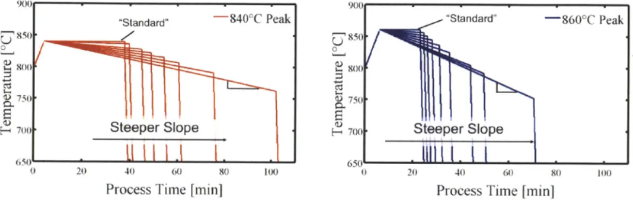
First, a standard phosphorus diffusion profile consisting of a ramp up from 800'C to a constant high-temperature plateau followed by an exponential cool from the high temperature plateau with an exponential time constant of 6 min, which is roughly equivalent to removing the wafer from the furnace to cool, was simulated. Phosphorus flow starts once the plateau temperature is reached.
dissolve to lower temperature where iron point defects are strongly driven to the phosphorus layer was considered. The continuously ramping phosphorus diffusion profile consists of a ramp up from 800'C to a peak temperature, then a ramp down to a lower temperature with no hold time and an exponential cool with a 6 min time constant. In order to simulate experimentally testable time-temperature profiles, a linear controlled cool slope from the peak temperature was chosen. The phosphorus diffusion starts at the peak of the profile.
901 "Standard" -840'C Peak 00 70' 700 Steeper Slope 0 20 40 60 80 100
Process Time [min]
(a) T(t) profiles for 840'C maximum temperature
"Standard"
-U
0
H 700 Steeper Slope
0 20 40 (A) 80
Process Time [min]
(b) T(t) profiles for 860'C maximum t 900, 0 6-J [-h 850 800 Tpeak 7 50r 7001 6; ~-
.1
"Standard"it.
-840
0C Peak
-860
0C
Peak-I
100Figure 4-1: Simulated 80 Q/sq. Phosphorus Diffusion Time-Temperature Profiles
The simulated time-temperature profiles for two different maximum temperatures,
860'C Peak
100
emperature
20 40 60 80
Process Time [min]
(c) A subset of T(t) Profiles for Comparison
"W% -- - .... p e7 Tcool
eper Slope
-0
Ste
840'C, a typical process temperature and 860'C, a higher temperature, are shown in Fig. 4-1. Fig. 4-1(c) shows a selection of profiles from (a) and (b) for easier com-parison. The parameters used for the simulations were typical for silicon solar cell material: surface concentration of phosphorus = 3x 1020 cm- 3, initial interstitial iron concentration = 101 cm 3 , initial total iron concentration = 1014 cm-3, initial iron
precipitate radius = 25 nm. For both standard and continuously ramping profiles, the
sheet resistance was held constant at 80 Q/sq., a typical or slightly high sheet resis-tance [42]. For each temperature, the standard profile is the one with the isothermal step and the shortest time because phosphorus diffuses in rapidly at high tempera-ture. All of the profiles with continuously ramping temperatures (no isothermal steps) are variations of the alternative approach. For the 840 C maximum temperature, the slope of the controlled cool portion of the profile varied from 00C/min (standard) to 0.8 C/min. For the 860'C maximum temperature, the slope of the controlled cool portion of the profile varied from 00C/min (standard) to 1.7 C/min. For the standard
profile, for each plateau temperature, the plateau time was adjusted until 80 Q/sq. was achieved. For the continuously ramping profiles, for each pair of peak tempera-ture and controlled cooling slope from the maximum temperatempera-ture, the controlled cool time was adjusted until 80 Q/sq.was achieved.
As the process temperature increases, the phosphorus diffusivity increases expo-nentially and therefore, the required process time to achieve a given sheet resistance decreases. Thus, for a higher target sheet resistance, shorter process times are re-quired. For the continuously ramping profiles, a higher temperature allows access to both higher and lower temperature for a given process time and sheet resistance. Ad-ditionally, somewhat counterintuitively, a steeper controlled cool (further deviation from standard) results in longer process times because as the temperature decreases, the phosphorus diffuses in less rapidly.
4.2
Calculated Effect of Standard and
Continu-ously Ramping Phosphorus Diffusion Time
-Temperature Profiles
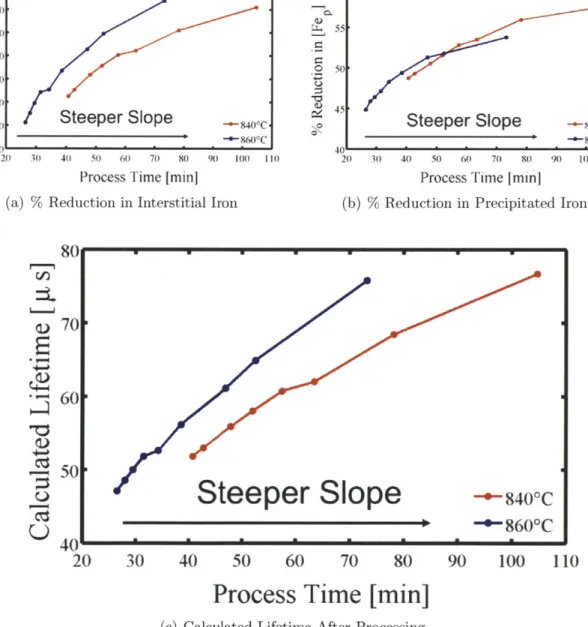
The final iron distribution and resulting effective bulk lifetime for each of the time-temperature profiles shown above were simulated using 12E.
The percent reduction of interstitial iron due to processing for each of the sim-ulated time-temperature profiles is shown in Fig. 4-2(a). Each of the points corre-sponds to one of the simulated time temperature profiles shown in Fig. 4-1(a) and (b). The simulation results indicate that for a given peak temperature, compared to the standard isothermal process, the longer processes with steeper ramping down slopes reduce iron point defects more effectively because the segregation coefficient, which is the driving force for iron to the phosphorus-rich layer, increases as temperature decreases, and the extra time is spent at high enough temperatures that iron can still diffuse through the silicon lattice relatively quickly.
The percent reduction in precipitated iron due to processing for each of the simu-lated time-temperature'profiles is shown in Fig. 4-2(b). For a given peak temperature, profiles with steeper controlled cool slopes reduce precipitated iron concentrations more effectively. For these parameters and profiles, for processes less than 55 min, a higher peak temperature can reduce precipitated iron concentration more effectively in less time. For processes longer than 55 min, lower peak temperature dissolves iron precipitates more effectively because the wafers are at a higher temperature for longer. It is beneficial to reduce the concentration of precipitated iron as long as the process can segregate the resulting point defects to the phosphorus-rich layer.
Consistent with the calculations of interstitial and precipitated iron concentra-tions, for a given peak temperature, steeper cooling slopes result in a higher effective lifetime. Additionally, higher maximum temperature processes can produce a higher effective lifetime in shorter time, as illustrated in Fig. 4-2(c). The simulated trends shown here hold for a wide parameter space relevant to solar cells.
30 40 50 60 70 90 90 100 0. a) 0 0 *0 a) I 10
Process Time [min]
(a) % Reduction in Interstitial Iron
20 30 40 50 60 70 80 90 100
Process Time [minI
(b) % Reduction in Precipitated Iron
80 70t 60 50t
401
86 0 C 20 30 40 50 60 70 80 90 100 110Process Time [min]
(c) Calculated Lifetime After Processing
Figure 4-2: Continuously ramping profiles are predicted to improve iron reduction and increase lifetime
4 C -2C a) -2 20 Steeper Slope - ' -*-600Cc 60) 55 50
Steeper Slope
8*)sC -8600C 110 0Steeper Slope
sit I c. --- 8400CChapter 5
Silicon Samples and Experimental
Methods
Two different silicon materials, monocrystalline and multicrystalline, were selected to experimentally compare the effect of a standard and an alternative phosphorus diffusion time-temperature profile on iron distribution and minority carrier lifetime. The multicrystalline silicon was etched to remove surface damage from sawing. Then, the resistivity and thickness of the samples were measured. Finally, the interstitial iron concentration, iron precipitate distribution, and minority carrier lifetime were measured before and after phosphorus diffusion processing.
5.1
Silicon Sample Selection
Silicon solar cell materials have a wide range of purity and defect levels. Thus, two different silicon materials were chosen based on their thickness and resistivity to experimentally test the effect of the simulated phosphorus diffusion profiles.
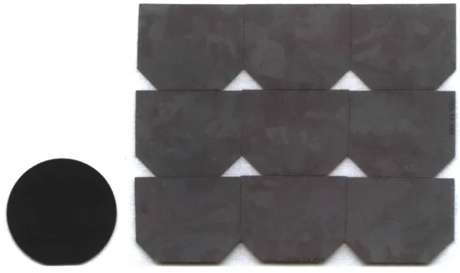
Representing relatively defect-free, pure material, eighteen wafers of two-inch di-ameter, 250-300 pm Czochralski-grown single-crystal, 1-10 Q-cm <100> silicon (CZ-Si) were selected. One side was polished and the other side was etched by the wafer manufacturer. Each sample was labelled with a diamond-tipped scribe pen on the polished side.
On the other hand, eighteen samples of multicrystalline silicon (mc-Si) were se-lected to represent defect-rich, impure material. The ingot from which the samples were chosen was grown from the tops of 40 other standard industrial ingots. Two ver-tically adjacent wafers were chosen from 90% ingot height and then laser cut into nine two-inch wide samples for sheet resistance, lifetime, and interstitial iron concentration measurements and a few smaller samples for total iron concentration and precipitated iron studies. A sample set separate from that used to characterize the lifetime and interstitial iron was used because the sheet resistance and lifetime measurements re-quire samples at least two inches in diameter, but the synchrotron beam line sample stage accommodates only small samples (up to about 1 cm2), and typically, less than
1 mm2 on each sample is scanned. Inductively coupled plasma mass spectrometry (ICP-MS), which is destructive and thus requires a dedicated sample, indicated that
the total as-grown iron concentration of these wafers is 1.1 x 1015 cm-3. All of the
mc-Si samples are expected to have similar total iron concentration because they come from two vertically adjacent wafers, essentially the same ingot height. Samples from the same wafer have different defect structures. Thus, the most similar samples are those from the same position on two vertically adjacent wafers. These mc-Si samples were labelled with the laser during the sample cutting process.
Optical scans of the two materials are shown in Fig. 5-1. Fig. 5-1(a) shows the polished side of a two-inch CZ-Si wafer. Fig. 5-1(b) shows the nine two-inch samples cut from one of the vertically adjacent full-size mc-Si wafers. The visible variations of gray are differently oriented crystal grains typical of cast mc-Si silicon.
The samples described above were put through the following experimental pro-cedure with careful attention to minimizing contamination during processing and reducing systematic error introduced by processing steps.
5.2
Saw Damage Etching Multicrystalline Silicon
The mc-Si wafers used in this experiment were sliced from an ingot with a sawing process, so the as-cut wafers have a surface layer of damaged silicon approximately
(b) 2" mcSi samples cut from one full wafer
Figure 5-1: Optical scans of silicon samples. (a) One of the two-inch CZ-Si samples.
(b) Nine two-inch-wide mc-Si samples cut from one full mc-Si wafer
10 ptm thick. This layer contains high concentrations of impurities from the sawing
slurry, which can contaminate the wafer during processing. Additionally, the silicon in this surface layer is mechanically damaged, which can lead to wafer breakage during processing. Therefore, this layer is chemically removed with the following chemical process:
" Dip in hydrofluoric acid (HF) for at least 30 seconds to remove native oxide. " CP4 chemical bath consisting of 70% nitric acid, 100% acetic acid, and 49% HF
in a ratio of 15:5:2.
" Dip in HF to remove oxide that forms during CP4 etch.
* Bath of 30% by weight potassium hydroxide (KOH) dissolved in water at room temperature for 1 minute.
* Dip in HF to remove oxide that forms during KOH bath.
Before and after each HF dip, the samples were rinsed with deionized water. This etch results in a fairly uniform reduction in thickness with a slightly higher etch rate at the sample edges. The reaction is exothermic, and the etch rate increases with temperature and the surface area of silicon in the bath. To verify how much silicon was removed during the etching step, the wafer sample thickness was measured with a micrometer and the wafer mass was measured with a mass balance before and after etching. Assuming the facial area of the wafer remains the same, the average thickness of the wafer was calculated by multiplying the initial thickness, do, by the ratio of the post-etching mass, metched, and pre-etching, mo mass as in Eq. 5.1. The wafer
thickness is also an input parameter for the resistivity and lifetime measurements and the 12E simulator.
detched do metched (5.1)
Tno
5.3
Bulk Resistivity Measurement
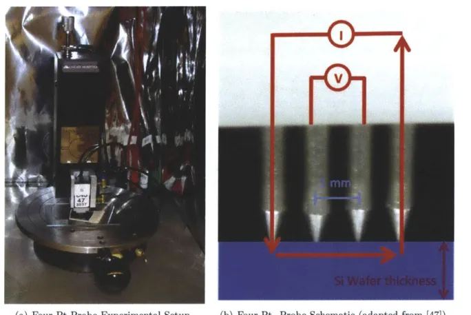
In typical p-type wafers for solar cells, the bulk resistivity is determined by the boron concentration. In addition to being a key electrical property of the material, the resistivity is an input to the minority carrier lifetime measurement and to 12E. A standard four-point probe configuration, shown in Fig. 5-2, was used to measure the resistivity. Current is passed through the outer two probes, and a potential difference is thereby induced between the two inner probes. The resistance is given by the slope of the curve of the induced voltage plotted against the range of currents swept. The resistivity is the resistance divided by the wafer thickness. The appropriate driving current must be used to achieve accurate resistance and resistivity measurements [46]. Higher currents allow for a higher signal-to-noise ratio, but if the current is too high, charge carriers can be injected into the sample, leading to an erroneous measurement.
(a) Four Pt Probe Experimental Setup (b) Four Pt. Probe Schematic (adapted from [47])
Figure 5-2: In a four-point probe configuration, current passes through the outer two probes and the sample, and the induced voltage is measured by the two inner probes. The probe spacing shown here is 1 mm.
5.4
Minority Carrier Lifetime Measurement
The minority carrier lifetime and the concentration of interstitial iron were measured before and after phosphorus diffusion. To reduce the recombination at the wafer surfaces, the surfaces are electrochemically passivated with aluminum oxide before the lifetime measurements [48].
1. Chemical Surface Clean in Preparation for Surface Passivation
Before depositing the aluminum oxide, the wafer surfaces were chemically cleaned with an RCA clean [49] consisting of the following steps:
" Dip in HF for at least 30 seconds to remove native oxide
* Bath of 5:1:1 deionized water: ammonium hydroxide: hydrogen peroxide for 10 minutes at 70'C (RCA1)
. . . .... ... . . .. .... ...
* HF dip to remove RCA1 silicon oxide
" Bath of 5:1:1 deionized water : hydrochloric acid : hydrogen peroxide for 10 minutes at 70'C (RCA2)
" Rinse in deionized water
Before and after each HF dip, the samples were rinsed with deionized water. The oxide that forms during the RCA2 bath is not etched before aluminum oxide deposition because it has been shown that the passivation is more effective with a surface oxide present
[50].
2. Atomic Layer Deposition of Aluminum Oxide for Surface Passivation
After surface cleaning, aluminum oxide was deposited on both sides of each wafer via atomic layer deposition (ALD) using a S200 Savannah at Harvard University's Center for Nanoscale Systems (CNS). First, small silicon chips were placed in the chamber and 5 nm of A1203 were deposited at 200'C. Next, the
samples were placed in the chamber, raised slightly above the chamber floor by the small silicon chips, and 20 nm of A1203 were deposited at 200'C [51]. To
densify the film and activate the passivation, the wafers were annealed at 375 C for 12 minutes in nitrogen [48].
3. Minority Carrier Lifetime Measurement
A tool for measuring the effective minority carrier lifetime of a silicon wafer
without electrical contacts is the Sinton WCT-120 Photoconductance Lifetime Tester [52]. Minority carrier lifetime can be expressed as in Eq. 5.2 [53]. The lifetime depends on the excess minority carrier density, An, the carrier gener-ation rate, G, and the derivative of the excess carrier density as a function of time.
An
T = (5.2)
G - dAn
dt
which the generation rate, G, is zero and one in which the excess carrier density, An, is in steady state, g =0. In each of the two following measurement modes, one of the two assumptions is fulfilled: transient photoconductance decay (PCD) and quasi-steady-state photoconductance
(QSSPC).
In PCD, the sample is flashed with a fast light pulse that decays in 1020 s. This fast flash results in a high concentration of excess carriers in the sample even after the flash has decayed. After the flash has terminated, the decaying conductivity of the silicon sample is measured as a function of time with the built-in radio frequency coil. During the measurement, no additional carriers are excited, so the generation rate, G, is zero. The excess carrier density as a function of time is calculated from the measured conductivity decay. The lifetime is then calculated using Eq. 5.3.
T ___A (5.3)
dAn dt
The fast flash decays in 1020 s, and the sample lifetime must be significantly longer than the flash decay time; thus, the PCD mode is valid for lifetimes greater than 100 ps.
On the other hand, in QSSPC mode, the sample is flashed with a light pulse that decays slowly, 12 ms. This slow flash results in a quasi-steady-state con-centration of excess carriers as the flash decays. While the flash decays, the flash intensity is measured with a built-in light sensor near the sample, and the conductivity is measured as a function of time. As in PCD mode, the excess carrier density as a function of time is calculated from the measured conduc-tivity. The generation rate is calculated from the light intensity reading and the user-provided optical constant, which estimates the fraction if incident light that is absorbed into the sample. The lifetime is then calculated using Eq. 5.4.
An
S=
An(5.4)
GBecause the flash decays in 12 ms, and the sample lifetime must be less than one tenth of the flash decay time; thus, the QSSPC mode is valid for lifetimes
less than 200 pts.
To achieve an accurate measurement, it is important to calibrate the tool, enter the sample properties in the software, and use the appropriate filters and flash settings as described in the manual [52].
5.5
Interstitial Iron Concentration Calculation
Point defects in silicon that pair Coulombically with substitutional dopants can be measured with a contactless, non-destructive technique that is sensitive at less than parts per billion and even parts per trillion [54]. Iron in boron-doped silicon is one such defect. In the dark at room temperature, positively charged interstitial iron, Fet, combines with negatively charged substitutional boron, BS-, to form iron-boron pairs, Fe-B, as described by chemical Eq. 5.5.
Fe+ + B- -+ FeB (5.5)
Strong illumination breaks Fe-B pairs into interstitial iron and substitutional boron. The energy level and capture cross section of Fet and Fe-B pairs are dif-ferent, so the lifetime associated with each chemical state is different.
The effective lifetime, T, when Fe-B pairs are dissociated can be expressed as the harmonic sum of the lifetime due to Fe-B pairs and other recombination pathways as expressed in Eq. 5.6. Similarly, the effective lifetime when Fe-B pairs are associated is expressed as in Eq. 5.7.
1 1 1(56
= -+ (5.6)
Tdiss TFe Tdiss,other
1 = + 1
(5.7)
T
Assuming the lifetime due to non-iron defects is the same for the associated and the dissociated states, the difference in lifetime due to Fe-B pairs and the lifetime due to interstitial iron, Fei, can be calculated by measuring the lifetime when the iron is in each state as shown in Eq. 5.8.
1 1 1 1 (5.8)
TFei TFeB Tdiss Tassoc
The concentration of Fei can be calculated from expression 5.9, where C is a function of the doping level, excess carrier density, and the fraction of Fe-B pairs that are associated [54, 55].
[Fe] =C( -
)
(5.9)TFei TFeB
Accordingly, two lifetime measurements were taken. First, the samples were flashed fifteen times with a 10-sun flash lamp to dissociate Fe-B pairs. Then life-time was measured. The samples were then left in the dark until the Fe-B pairs reassociated at which time the lifetime was remeasured. The association time con-stant, Tassoc, given by Eq. 5.10, depends on the bulk doping concentration, NA, and the temperature, T [56]. For the CZ-Si, the association time was 7.5 hours and the doping concentration was 3.7x 1015 cm-3. For the mc-Si, the association time was
1.25 hours and the doping concentration was 2.65x 1016 cm-3.
T 0.66eV
Tassoc = 5 x 10⁵ N exp( k ) (5.10)
NA kBT
5.6
Phosphorus Diffusion
After the as-grown samples have been characterized as described above, the aluminum oxide is removed with hydrofluoric acid, and the samples are RCA cleaned as described in section 5.4, with the addition of a final hydrofluoric acid dip right before loading into the phosphorus diffusion furnace.
the phosphorus diffusion temperature, diffuse phosphorus into the silicon at that high temperature, allow the phosphorus to soak into the wafers while flowing nitrogen and oxygen, purge the furnace with oxygen, cool and unload the wafers. The phosphorus oxychloride bubbler temperature, gas flow rates, furnace size and geometry, and the history of processing carried out in the furnace are all factors that affect the result of the phosphorus diffusion process. However, in this experiment, the time-temperature profile was the focus.
The orientation of the two sets of wafers was designed to maximize the uniformity of the flow. The samples were placed vertically to active a double-sided diffusion. Several dummy wafers were placed in the outermost slots, then the CZ-Si test wafers were split into two groups and were placed just inward of the dummy wafers, and finally the mc-Si wafers were placed in the middle.
5.7
Sheet Resistance Measurement
After the phosphorus diffusion step, the sheet resistance of the phosphorus-diffused layer is measured with a four-point probe setup as described in section 5.3 with the
appropriate driving current range. For the measurements performed for this exper-iment, the phosphosilicate glass (PSG) that forms during phosphorus in-diffusion was not etched. Typically, the presence of the PSG does not affect the sheet resis-tance measurement because the probe tips penetrate through the PSG to contact the phosphorus-diffused silicon below. There is usually variation across the wafer faces
and between the fronts and backs of the wafers due to heterogeneity in the gas flows. Additionally, the sheet resistances measured on CZ-Si are typically higher than that of the mc-Si because phosphorus preferentially diffuses along grain boundaries more rapidly [57]. Accordingly, to characterize the average and standard deviation of the sheet resistance, each wafer was measured on both sides in three different locations.
Finally, the phosphorus-diffused emitter layer was chemically etched with CP4, and the sample thickness, the lifetime, and the interstitial iron concentration were remeasured as described above.
5.8
Characterizing the Distribution of Precipitated
Iron with Synchrotron-Based micro-X-Ray
Flu-orescence
In parallel with the measurements of minority carrier lifetime and iron point defects described above, iron precipitates in two samples of the mc-Si material were measured with synchrotron-based micro-X-ray fluorescence spectroscopy ( -XRF). From each of the two vertically adjacent wafers from which the eighteen larger samples originated, one sample was selected from the same sample position. The total iron concentration
of both synchrotron samples was assumed to also be 1.1 x 1015 cm-3 as was measured
by ICP-MS on a different sample from the same wafer.
After the samples were laser cut from the full size wafer, they were saw damage etched with CP4 and RCA cleaned. Then the as-grown precipitated iron distribu-tion was measured at the synchrotron at a random angle grain boundary. Typically, high misorientation grain boundaries are measured because they are favorable het-erogenous nucleation sites for metallic precipitates [57]. Additionally, scanning grain boundaries instead of intragranular regions ensures that the unique, exact location of the scan is known. Electron backscatter diffraction (EBSD) is used to characterize the grain structure and grain boundary type of the samples [58]. A sample that was in a third vertically adjacent wafer from the same horizontal position was polished, and grain orientations and grain boundary types were determined by EBSD. The samples were then RCA cleaned again and phosphorus diffused. Samples were pro-cessed vertically in a custom-made quartz try to achieve a double-sided diffusion for better comparability with the larger samples that were used for lifetime and inter-stitial iron measurements. The phosphosilicate glass that forms during phosphorus diffusion was removed with hydrofluoric acid. Finally, both samples were returned to the synchrotron, and the exact same region was measured again, allowing for a direct comparison before and after processing.


![Figure 3-1: Diagram of Impurity-to-Efficiency simulation tool (reprinted from [37])](https://thumb-eu.123doks.com/thumbv2/123doknet/14347003.500221/28.918.153.745.151.533/figure-diagram-impurity-efficiency-simulation-tool-reprinted.webp)