Properties of Dual-Phase V
3Ga"
Michelle E. Jamer,1 Brandon Wilfong,1 Vasiliy D. Buchelnikov,2, 3 Vladimir V. Sokolovskiy,2, 3 Olga N.
Miroshkina,2, 4Mikhail A. Zagrebin,2, 3, 5Danil R. Baigutlin,2, 4 Jared Naphy,1 Badih A. Assaf,6 Laura H. Lewis,7 Aki Pulkkinen,8, 4 Bernardo Barbiellini,4, 9Arun Bansil,9and Don Heiman9
1)
Physics Department, United States Naval Academy, Annapolis, MD 20899, USA
2)
Faculty of Physics, Chelyabinsk State University, 454001 Chelyabinsk, Russia
3)
National University of Science and Technology "MISiS", 119049 Moscow, Russia
4)Department of Physics, School of Engineering Science, LUT University, FI-53850 Lappeenranta,
Finland
5)
National Research South Ural State University, 454080 Chelyabinsk, Russia
6)
Physics Department, University of Notre Dame, South Bend, IN 46556, USA
7)Chemical Engineering Department, Northeastern University, Boston, MA 02115,
USA
8)
Département de Physique and Fribourg Center for Nanomaterials, Université de Fribourg, CH-1700 Fribourg, Switzerland
9)
Physics Department, Northeastern University, Boston, MA 02115, USA (Dated: 20 July 2020)
1. Details and Results of the VASP calculations
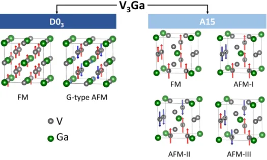
The geometric optimization and ground state calculations were performed for two structures (D03 and β-W A15) of V3Ga, which are experimentally observed. In the case of the D03 structure, the 16-atom supercell was considered in which Ga atoms locate at 4a (0.0, 0.0, 0.0) Wyckoff positions and V atoms occupy 4b (1/2, 1/2, 1/2) and 8c ((1/4, 1/4, 1/4) and 3/4, 3/4, 3/4)) sites. For the A15 structure, a six-atom supercell was used in which the two Ga atoms occupy the 2a sites and the six V atoms locate at 6c sites. Concerning the magnetic subsystem, ferromagnetic (FM) and antiferromagnetic (AFM) spin alignments of V atoms were considered. For the D03 structure, FM and AFM G-type orders were considered along the lines Ref.1, while for the A15 structure, FM and three AFM orders were computed as suggested in Ref.2. The crystal structures and magnetic configurations considered are illustrated in Fig. S1. In order to emphasize the AFM state, V atoms located at different sites are labelled as 1, 2, and 3.
FIG. S1. Various magnetic ordering of D03 and A15 structures of V3Ga on which computations were carried out. V atoms
located at different sites are labelled 1, 2, and 3.
In order to understand the robustness of our results we carried out computations using four different schemes for treating exchange-correlation effects: LDA-PZ3, GGA-PBE4–6, GGA+U and meta-GGA-SCAN7–9. For the GGA+U
scheme, the values of Hubbard-repulsion U and Hund-exchange integral J for the V atoms were taken to be 2 eV and 0.67 eV, respectively following He et al.2. The PAW-pseudopotentials were taken with valence-electron config-urations as follows: 3s23p64s23d3 for V atoms and 3d104s24p1 for Ga atoms. The 10×10×10 k-point-grid used in the computations was generated using via the Monkhorst-Pack scheme. The kinetic-energy cutoff for the augmented plain waves was taken to be 750 eV. The Methfessel-Paxton smearing method10 was used with a width of 0.2 eV in geometry optimization runs, and the tetrahedron smearing method with Blóchl corrections11 was deployed in self-consistent calculations. Total energies were converged to an accuracy of 10−8 eV. The convergence criterion in the optimization for the residual forces was 10−7 eV/Å. Results for the D03 and A15 structures of V3Ga are presented in Tables S1 and S2.
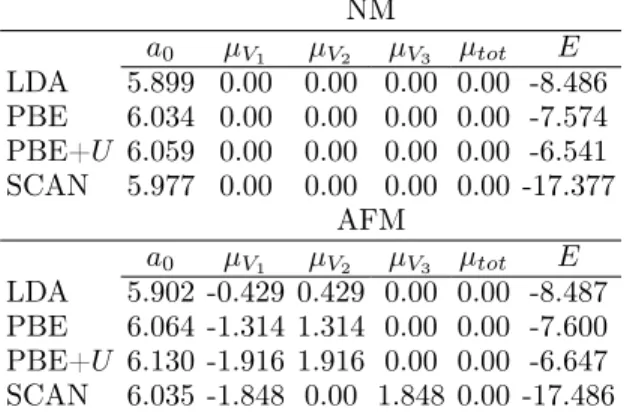
TABLE S1. Equilibrium lattice parameter (a0 in Å), partial and total magnetic moments (µVi and µtot in µB/f.u.), and total
energies (E in eV/atom) of non-magnetic (NM) and AFM phases of D03structure. Notice, the initial FM order was converged
to the non-magnetic (NM) one.
NM a0 µV1 µV2 µV3 µtot E LDA 5.899 0.00 0.00 0.00 0.00 -8.486 PBE 6.034 0.00 0.00 0.00 0.00 -7.574 PBE+U 6.059 0.00 0.00 0.00 0.00 -6.541 SCAN 5.977 0.00 0.00 0.00 0.00 -17.377 AFM a0 µV1 µV2 µV3 µtot E LDA 5.902 -0.429 0.429 0.00 0.00 -8.487 PBE 6.064 -1.314 1.314 0.00 0.00 -7.600 PBE+U 6.130 -1.916 1.916 0.00 0.00 -6.647 SCAN 6.035 -1.848 0.00 1.848 0.00 -17.486
FIG. S2. Exchange coupling constants Jijas a function of the distance (d/a) between the atoms i and j in the V3Ga with D03
structure at the equilibrium lattice parameter
2. Details and Results of the SPR-KKR calculations
The Heisenberg exchange-coupling parameters (Jij) were obtained by using the spin-polarized scalar-relativistic (SP-SREL) Dirac-Hamiltonian as part of the SPR-KKR (spin-polarized relativistic Korringa-Kohn-Rostoker) package12.
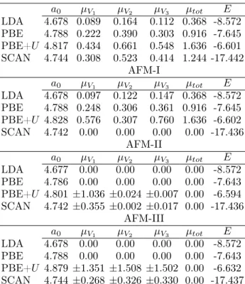
TABLE S2. The equilibrium lattice parameter (a0 in Å), partial and total magnetic moments (µVi and µtot in µB/f.u.), and
total energy (E in eV/atom) of FM and AFM phases of A15 structure.
FM a0 µV1 µV2 µV3 µtot E LDA 4.678 0.089 0.164 0.112 0.368 -8.572 PBE 4.788 0.222 0.390 0.303 0.916 -7.645 PBE+U 4.817 0.434 0.661 0.548 1.636 -6.601 SCAN 4.744 0.308 0.523 0.414 1.244 -17.442 AFM-I a0 µV1 µV2 µV3 µtot E LDA 4.678 0.097 0.122 0.147 0.368 -8.572 PBE 4.788 0.248 0.306 0.361 0.916 -7.645 PBE+U 4.828 0.576 0.307 0.760 1.636 -6.602 SCAN 4.742 0.00 0.00 0.00 0.00 -17.436 AFM-II a0 µV1 µV2 µV3 µtot E LDA 4.677 0.00 0.00 0.00 0.00 -8.572 PBE 4.786 0.00 0.00 0.00 0.00 -7.643 PBE+U 4.801 ±1.036 ±0.024 ±0.007 0.00 -6.594 SCAN 4.742 ±0.355 ±0.002 ±0.017 0.00 -17.436 AFM-III a0 µV1 µV2 µV3 µtot E LDA 4.678 0.00 0.00 0.00 0.00 -8.572 PBE 4.788 0.00 0.00 0.00 0.00 -7.643 PBE+U 4.879 ±1.351 ±1.508 ±1.502 0.00 -6.632 SCAN 4.744 ±0.268 ±0.326 ±0.330 0.00 -17.437
For these calculations, the optimized lattice parameter was obtained by a VASP-based calculation for the FM phase of D03 structure. Here, calculations were carried out for a unit cell of D03 consisting of four atoms (3 V and 1 Ga). The exchange-correlation energy was treated by the GGA-PBE parameterization5. For the self-consistency cycles, 2300 k -points were generated by a k -mesh grid of 453. The angular momentum expansion (lmax)was restricted to three. The magnetic exchange constants were calculated on a k -mesh grid of 57 × 57 × 57 with 4495 k -points. All calculations converged to 0.01 mRy for total energy. Dependence of the exchange-interaction parameters Jij on the distance between the atoms d/a is shown in Fig. S2.
Here, the positive exchange constants (Jij> 0) imply FM coupling, whereas negative values (Jij < 0) indicate AFM coupling. Large FM interactions are seen between the nearest neighbor V1-V1and V2-V2atoms. Magnitudes of both these couplings are about of 3 meV. The couplings are zero in the third and farther coordination shells. The strongest AFM interaction (-5.5 meV) occurs between the nearest V1 and V2 atoms in different sublattices. All interactions with V3 atoms are close to zero (Table 1).
3. Details and Results of the Monte Carlo simulations
To extend the zero-temperature ab initio results to finite temperatures, we further performed Monte Carlo (MC) simulations on the classical three-dimensional Heisenberg model (H = flP
ijJijSiSj) in zero magnetic field. Here, Si= (Six, S
y i, S
z
i) is a classical Heisenberg spin variable |Si| = 1 and Jijare the exchange-coupling constants (positive for FM and negative for AFM interactions). The calculated exchange parameters (Jij) and partial magnetic moments (µi) were taken as input parameters. Values of Jij’s show long-range oscillations as a function of the distance between the atoms (d/a). We restricted exchange interactions up to the sixth coordination shell for all interaction pairs.
The MC simulations were carried out for a lattice with a unit cell consisting of 3925 atoms (1099 Ga and 2826 V atoms) with periodic boundary conditions. The Metropolis algorithm13 was used where a new, random spin direction was chosen and the resulting energy change was calculated. Changes in the independent spin variables Si = (Sx
i, S y i, S
z
i) were accepted or rejected based on the single-site transition probability W = min [1, exp (−∆H/kBT )]. As the time step, we used one MC step consisting of N attempts to change the spin variables. A new spin direction can be chosen by randomly choosing new spin components. The spin components were chosen in the following manner13. Two random numbers r1and r2are chosen from the interval [0, 1] to produce a vector with two components ζ1= 1−2r1
FIG. S3. Temperature variation of the partial magnetization curves for V3Ga in the D03 structure at zero magnetic field.
and ζ2= 1 − 2r2. Length of the vector is determined by ζ2= ζ12+ ζ 2
2 and if ζ
2< 1, then a new spin vector is computed with components Six= 2ζ1 p 1 − ζ2, Sy i = 2ζ2 p 1 − ζ2, Sz i = 1 − 2ζ 2.
At each temperature properties (internal energy of the system hHi and magnetic order parameter hmi) were esti-mated allowing 105MC steps and 104 thermalization steps and were averaged over 2250 configurations for each 400 MC steps. The simulation started from the ferromagnetic phase with Sz
i = 1. The magnetic order parameter is defined as follows:
mα= 1 Nα X i q (Siα,x)2+ (Siα,y)2+ (Siα,z)2,
where α denotes the V1, V2and V3atoms and Nαthe total number of α atoms; i runs over the corresponding lattice sites of the α atoms. The resulting temperature dependencies of partial magnetizations of V1,2 for V3Ga with D03 alloy at zero magnetic field is shown in Fig. S3.
In order to estimate the Neél temperature, we plotted m (T ) = (mα)1/β(T ) function, which approximately decreases linearly with increasing temperature. The Neél temperature can then be estimated from the intersection of m with the T axis. Here, mαis the partial magnetization of V
1 and V2 atoms and β is the critical index. Note, in the case of the three-dimensional Heisenberg model the β exponent is equal to 0.3646. In this way, we obtain the estimated Neél temperature TN = 587 K.
4. Results of Disorder Calculations
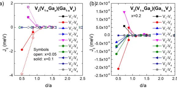
Effects of disorder on the Neél temperature were obtained using the SPR-KKR package based on the KKR-CPA approach. The degree of disorder in the atomic sublattices was quantified by x, which is defined as the fraction of Ga atoms that are exchanged for nonmagnetic V atoms ( V3), where the nonmagnetic V atoms lie between the two antiferromagnetically coupled magnetic V atoms (V1 and V2). Results are given in Table S3 for x = 0 to 0.2. For all values of x, the V1 and V2 magnetic atoms have opposite orientation and equal magnetic moments, while the V3 moment is zero.
Calculated magnetic exchange-coupling parameters (Jij) for the D03 phase for various degrees of disorder x are presented in Fig. S4. Dominant exchange interactions, FM V1-V3 and V2-V2, and AFM V1-V2, weaken substantially with increasing disorder. For x = 0.2, all Jij are almost zero ( Fig. S4(b)). These results suggest that the Neél temperature will decrease with rising disorder. Mean-field calculations using these Jij’s show a decrease in the Neél
FIG. S4. Exchange coupling constants Jijas a function of the distance (d/a) between the atoms i and j for D03 phase of V3Ga
for several different values of disorder x.
TABLE S3. Partial magnetic moments of Vi atoms and the Neél temperatures calculated for D03 phase of V3Ga for different
degrees of disorder x. Note, that x = 0 refers to the ordered D03structure.
Degree of disorder µV1 µV2 µV3 µV4 µtot TN
0 -1.161 1.161 0.00 - 0.00 630.0
0.05 -0.997 0.997 0.00 0.00 0.00 414.5 0.1 -0.720 0.720 0.00 0.00 0.00 189.3 0.2 0.002 0.002 0.00 0.00 0.00 0.00
temperature from TN = 630 K at x = 0 to TN = 0 K at x = 0.2 (Table S3). We would expect a similar behavior from Monte Carlo simulations.
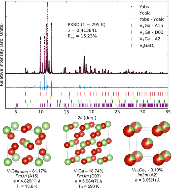
5. Results of Rietveld X-ray diffraction analysis
X-ray diffraction from the V3Ga sample was taken at Beamline 11-BM at the Advanced Photon Source at Argonne National Lab using a wavelength of λ = 0.413841 Å. The sample was rotated continuously. Fig. S5 shows the XRD data and the results of the subsequent Rietveld and Pawley fitting procedures.14 The experimental data is shown by points and the fit is shown by the pink curve. The lower blue curve plots the experimental data minus the Rietveld fit. Here, only the A15, D03 and A2 phases were included in the Rietveld fitting procedure. The A2 phase is a disordered D03 phase where the V and Ga atoms are randomly exchanged. When we included only these three phases, our analysis indicated that there was still another missing phase. A search of relevant V, Ga and V-Ga binary phases (V6Ga5, V6Ga7, V2Ga5) were unable to accurately index the remaining peaks. Thus, an expanded search to contain impurity oxide phases was done. In this way, we determined that the remaining peaks could be accurately indexed to the reported oxide impurity phase, V3GaOx.15The structure of the V3GaOxphase has not been rigorously reported; however, the previous work has discussed the structure as Cu3Au-type perovskite with Ga at the corners, V at the face centers and O at the body center. From this, a structure was built and the space group determined through the use of the Python Materials Genomics library.16 Since the structure of the V3GaOx has not been determined and its existence as a minor impurity phase has not been clearly established in the current work, it’s contribution to the X-ray diffraction pattern was modeled only by a Pawley refinement procedure. As such, the weight fraction of the V3GaOx phase could not be determined and, therefore, all weight fractions for the A15, D03, and A2 phases are reported relative to each other. The results of the fitting procedure provided the following approximate percentages of the various phases: 81% in the A15 phase, 18% in the D03phase, and 0.1% in the A2 phase. An attempt to include the assumed structure for the V3GaOx phase for Rietveld refinement yielded an approximate weight fraction on the order of 30 - 40%.
6. Analysis of superconductivity of the A15 phase
Additional analysis of the as-synthesized superconducting properties of A15 V3Ga revealed a superconducting critical temperature of 13.6 K and a superconducting volume fraction at 2 K of approximately 90% as shown in
FIG. S5. High resolution synchrotron X-ray diffraction patterns for the as-grown V3Ga ingots collected at T = 295 K. Red
and green tick marks represent the targeted V3Ga , A15 and D03 phases respectively. Orange tick marks represent impurity
A2 phase and purple tick marks show the existence of an impurity oxide phase, V3GaOx. Also shown are the calculated,
observed, and differences curves from Rietveld analysis. Crystal structures, the corresponding extracted lattice parameters and the elemental composition from Rietveld analysis, and the relevant transition temperature for each phase are shown below the XRD data.
FIG. S6. Temperature dependence of the dimensionless magnetic susceptibility at 0.05 T and the isothermal magnetization at 10 K of the V3Ga sample mixture measured on the as-synthesized polycrystalline material.
Fig. S6. This was calculated from the density and phase fraction extracted from Rietveld analysis from synchrotron X-ray diffraction data for the A15 phase. Isothermal magnetization at 10 K revealed an upper critical field, Hc2 of about 3.5 T which is significantly lower than previous reports.17,18 This is mainly due to the lower Tc of our sample, but could also be affected by a number of factors such as stoichiometric changes in the as-synthesized A15 V3Ga phase as well as the coexistence of another magnetic phase due to the V3Ga D03 phase in the as-synthesized sample. Thus, the assignment of an Hc2 value to the A15 V3Ga phase cannot be done in a rigorous way. However, the extracted superconducting volume fraction and superconducting critical temperature matches with expectations.
FIG. S7. X-ray absorption spectra at the vanadium L-edge from the V3Ga ingots collected at 89 K. The L3 and L2 edges are
7. X-ray Absorption Spectrum (XAS)
X-ray absorption spectra (XAS) at the vanadium L3 and L2 edges were taken using the U4B beamline at the National Synchrotron Light Source at Brookhaven National Laboratory in the total-electron-yield (TEY) mode. The field-dependent measurements were taken at various energies, including energies above, below and at the L2 and L3 edges of the V atoms. X-ray magnetic circular dichroism (XMCD) of the V3Ga ingot was also taken but there was no detectable signal (<0.01%) when comparing data obtained using right- and left-circular polarizations of radiation, and using the complementary technique of changing magnetic field direction. In Fig. S7, the L3 and L2 edges are marked. The XAS and XMCD spectra were taken at temperatures between 12.5 K and 300 K, both below and above the superconducting transition, and no ferromagnetic signal was detected.
1I. Galanakis, S. Tirpanci, K. Özdoğan, and E. Şaşıoğlu, Phys. Rev. B 94, 064401 (2016). 2B. He et al., Phys. Stat. Sol. (RRL) 13, 1900483 (2019).
3J. P. Perdew and A. Zunger, Phys. Rev. B 23, 5048 (1981). 4J. Perdew, Physica B: Conds. Mater. 172, 1 (1991).
5K. Burke, J. Perdew, and M. Ernzerhof, Int. J. Quant. Chem. 61, 287 (1997). 6J. Perdew, K. Burke, and M. Ernzerhof, Phys. Rev. Lett. 77, 3865 (1996).
7J. P. Perdew, S. Kurth, A. c. v. Zupan, and P. Blaha, Phys. Rev. Lett. 82, 2544 (1999). 8J. Tao, J. P. Perdew, V. N. Staroverov, and G. E. Scuseria, Phys. Rev. Lett. 91, 146401 (2003). 9J. Sun, A. Ruzsinszky, and J. P. Perdew, Phys. Rev. Lett. 115, 036402 (2015).
10M. Methfessel and A. T. Paxton, Phys. Rev. B 40, 3616 (1989).
11P. E. Blöchl, O. Jepsen, and O. K. Andersen, Phys. Rev. B 49, 16223 (1994). 12H. Ebert, D. Ködderitzsch, and J. Minár, Repts. Prog. Phys. 74, 096501 (2011).
13D. P. Landau and K. Binder, A Guide to Monte Carlo Simulations in Statistical Physics, Cambridge University Press, 2 edition, 2005. 14A. A. Coelho, J. Appl. Crystallogr. 51, 210 (2018).
15R. Maier, Y. Uzel, and H. Kandler, Zeitschrift für Naturforschung A 21, 531 (1966). 16S. P. Ong et al., Computational Materials Science 68, 314 (2013).
17S. Foner, E. McNiff Jr, S. Moehlecke, and A. Sweedler, Sol. State Commun 39, 773 (1981). 18D. Decker and H. Laquer, J. Appl. Phys. 40, 2817 (1969).