THE EFFECT OF OXYGEN PARTIAL PRESSURE ON THE EPITAXY OF CERIUM OXIDE FILMS DEPOSITED ON NICKEL SUBSTRATES
by
Todd S. Stefanik
B.S., Ceramic Engineering (1995) New York State College of Ceramics
at Alfred University
Submitted to the Department of Materials Science and Engineering in Partial Fulfillment of the Requirements for the Degree of
Master of Science in Materials Science and Engineering at the
Massachusetts Institute of Technology June 1998
@ 1998 Massachusetts Institute of Technology All rights reserved
Signature of Author...
Certified by...
Accepted by ...
Department/of Materials Science and Engineering May 8, 1998
( Michael J. Cima
Sumitomo Electric Industries Professor of Engineering Thesis Supervisor
... ... ... Linn W. Hobbs John F. Elliott Professor of Materials Chairman, Departmental Committee on Graduate Students MASSACHUSETTS INSTITUTE OF TECHNOLOGY
MAY 211998
I IRPAI. MASSACHUSETTS INSTITUTE OF TECHNOLOGYAPR 051999
LIBRARIES keCro-The Effect of Oxygen Partial Pressure on the Epitaxy of Cerium Oxide Films Deposited on Nickel Substrates
by
Todd S. Stefanik
Submitted to the Department of Materials Science and Engineering on May 8", 1998 in partial fulfillment of the requirements for the
degree of Master of Science
Abstract
Epitaxial deposition of cerium oxide thin films on nickel substrates by electron beam evaporation of cerium oxide and reactive evaporation of cerium metal was examined. Epitaxial films were produced using both techniques. The mechanisms governing each deposition technique were examined using in-situ electrical conductivity measurements. Electrical characterization revealed that in all cases in which epitaxial cerium oxide is deposited on nickel, the species deposited is an oxide, not a metallic phase.
The critical factor in determining the epitaxy of a cerium oxide film deposited on nickel was determined to be oxygen partial pressure. During evaporation of cerium oxide, care must be taken to ensure that the total oxygen partial pressure of the background gas does not increase enough to oxidize the substrate, thereby destroying the epitaxial surface. When determining this stability point, it is critical to account for oxygen evolved by the cerium oxide source. During reactive evaporation of cerium metal, the oxygen level must be high enough to oxidize the metallic deposition flux before it reaches the substrate or the cerium metal alloys with the nickel substrate. The oxygen level must be low enough to prevent formation of nickel oxide prior to deposition.
Reproducibility problems hinder the usefulness of reactive evaporation of cerium metal on nickel as an industrial scale production technique. Therefore, evaporation of cerium oxide for bulk production should be investigated. Although maintaining a
sufficiently low oxygen partial pressure during evaporation of cerium oxide is not trivial, maintaining the oxygen partial pressure both high enough to oxidize cerium and low enough to prevent nickel oxide formation during reactive evaporation requires more stringent control than that necessary for oxide evaporation.
Thesis Supervisor: Michael J. Cima
TABLE OF CONTENTS Page TITLE PAGE 1 ABSTRACT 2 TABLE OF CONTENTS 3 LIST OF FIGURES 5 ACKNOWLEDGMENTS 9 CHAPTER 1: INTRODUCTION 10
Superconductor material systems 10
Long length conductors 11
Epitaxialfilms 11
Ion beam assisted deposition 11
Deformation texturing 12
Buffer layer architectures 13
Purpose of the buffer 13
Noble metals 14
Direct oxide deposition 14
Thesis motivation 15
CHAPTER 2: EXPERIMENTS 16
Processing 16
Substrates 16
Deposition chamber 17
Electron beam evaporator 20
Deposition conditions 23
Characterization 23
Deposition rate and film thickness 23
Crystallographic orientation 25
CHAPTER 3: RESULTS 27
Crystallographic orientation 27
Deposition from cerium on nickel 27
Deposition from oxide on nickel 27
Reproducibility issues 30
Epitaxial Reproducibility 30
Sources of variation 34
Experimental evidence for the variation of background
gas composition 36
Film thickness calculations 39
CHAPTER 4: DISCUSSION AND TESTING OF MECHANISMS 43
Wetting angle mechanism 43
Reduced CeO2 deposition 46
Thermodynamics of reduced CeO2 deposition 48
Electrical characterization 48
Experimental setup 50
Control depositions 52
Electrical response during epitaxial depositions from cerium 56
Electrical response during deposition from reduced CeO2 58
Substrate contamination mechanism 60
Thermodynamics of nickel oxide formation/reduction 60
Depositions from CeO2 after purging with forming gas 61
Oxygen evolution from the source 61
Description of active mechanisms 65
CHAPTER 5: CONCLUSIONS 68
APPENDIX A: UV/VIS THICKNESS MACRO 70 APPENDIX B: OXYGEN EVOLUTION FROM A CeO2 SOURCE 101 APPENDIX C: NICKEL OXIDE STABILITY DURING CeO2 DEPOSITION 104
APPENDIX D: OXYGEN FLOW NECESSARY TO OXIDIZE
CERIUM DURING METALLIC DEPOSITION 106
LIST OF FIGURES
Figure # Page #
Chapter 2
2.1 Diagram of the clamping system used to mechanically 18 mount nickel substrates for deposition.
2.2 Two shutter configurations possible when performing 19 depositions. The open/closed configuration (a) was used to
deposit several films of different thickness during the same deposition. The slot configuration (b) was used to deposit multiple films at different times during a deposition.
2.3 Chamber pressure as a function of gas flow at the control 21 ion gauge (located beneath the high vacuum valve) and at
the top of the chamber.
2.4 A schematic of the deposition chamber used during this 22 study.
2.5 A typical UVNis transmission spectrum from a CeO2 film 24 on silica glass showing curve fits generated during
calculation of film thickness.
2.6 The arrangement of (200) and (111) poles in a cubic 26 material such as CeO2 or nickel is shown in (a). Shown in
(b) and (c) are the experimental setups for 0/20 scans and P scans, respectively. The angles 0, 20, 3, and X are
identified.
Chapter 3
3.1 Diffraction patterns of a CeO2 film deposited on nickel 28 from a cerium metal source. A 0/20 pattern is shown in
(a). The (111) P scans of the nickel substrate and epitaxial CeO2film are shown in (b).
3.2 0/20 diffraction pattern for a CeO2 film deposited on a 29 nickel substrate from a CeO2 source (a). Shown in (b) is
the (200) P scan of the CeO2 film.
3.3 Diffraction patterns of a CeO2 film deposited on LaAlO3 31 from a cerium metal source. Depicted in (a) is a 0/20 scan,
while (b) shows the (111) CeO2
3
scan.3.4 Diffraction patterns of a CeO2 film deposited on LaA1O3 32 from a CeO2 source. The 0/20 scan is shown in (a). The
(111) CeO2 3 scan is shown in (b).
3.5 The 0/20 scans shown demonstrate the lack of 33 reproducibility in CeO2 films deposited by reactive
evaporation of cerium metal on single crystal nickel substrates. All three films were processed under the same conditions (1
A/s,
6500C ,1-2 sccm Ar/5%H2). The resulting films demonstrated (200) epitaxial alignment, (111) wire texture, and alloying of the cerium metal with the nickel substrate, respectively.
3.6 The 0/20 scans of CeO2 films on LaA10 3 substrates 35 demonstrate a lack of reproducibility of epitaxy when
depositing from a cerium metal source. Oxygen content of the background gas increases from the top scan to the bottom scan, yet only the film processed in a gas composition of intermediate oxygen partial pressure exhibits a polycrystalline component.
3.7 CeO2 films deposited on nickel substrates from a cerium 37 metal source undergo epitaxial growth at low film
thickness, but lose this epitaxial relationship as film thickness increases, as indicated by X-ray 0/20 diffraction patterns.
3.8 CeO2 films deposited from a CeO2 source maintain an 38 epitaxial relationship to the substrate, independent of film
thickness, as indicated by X-ray 0/20 patterns. The films were deposited on nickel substrates capped with a thin epitaxial layer of CeO2deposited from cerium metal.
3.9 X-ray 0/20 patterns for two films deposited on nickel from 40 a cerium metal source. The first film was deposited
immediately after the cerium source was conditioned, while the second film was deposited after three hours of
evaporation. The first film exhibits (200) epitaxial CeO2, while the second shows evidence of alloying between the cerium metal and nickel substrate.
3.10 The figure shows average deposition rates for CeO2 films 42 deposited on silica glass substrates as calculated from
optical thickness measurements as a function of total film thickness. The deposition rate programmed into the thickness monitor was 1.0 A/s, while the actual deposition rate achieved was 0.91 A/s.
Chapter 4
4.1 Surface contact area of a film deposited on a flat substrate 44 varies as a function of the wetting angle (4) of the
deposited species on the substrate material. For high wetting angles, as depicted in (a), there is very little substrate contact, hindering epitaxial growth. For low wetting angles (b), substrate contact area is much higher, making epitaxial growth more probable.
4.2 CeO2 film deposited on a glass substrate by reactive 45 evaporation of cerium metal. The favored alignment when
no epitaxial relationship with the substrate exists is (111) wire texture, as indicated by the 0/20 scan (a) and (200) P scan (b) shown.
4.3 X-ray 0/20 and (111) P scans of a CeO2 film deposited 47 from a CeO2 source on a nickel substrate ((a) and (b),
respectively). The CeO2 source was conditioned in forming gas, then excess oxygen in the chamber was removed using cerium metal as a getter prior to deposition from the pre-conditioned CeO2 source. The diffraction data indicate that the film grew epitaxially on the nickel
4.4 Ellingham diagram for NiO and CeO2. The stability of 49 these oxides as a function of temperature and gas
composition may be read from the diagram.
4.5 A schematic of the substrate geometry (a) and electrical 51 circuit (b) used to perform in-situ conductivity
measurements of films during deposition.
4.6 Voltage response of films deposited from cerium metal 53 after a long cerium metal purge of the chamber. 1000A of
material was deposited in 5 seem forming gas.
4.7 Voltage response of films deposited from CeO2 in ambient 55 atmosphere (no gas flowing).
4.8 Voltage response of films deposited from cerium metal in a 57 background gas composition consisting of 0.7 sccm
Ar/5%H2 + 0.3 sccm Ar/8%02.
4.9 Voltage response of films deposited from CeO2 after 59 conditioning the CeO2 source in forming gas and removing
residual oxygen from the chamber using cerium metal as a getter.
4.10 X-ray 0/20 scans of films deposited on nickel from CeO2 62 before and after purging the chamber with 12 sccm forming
gas for 6 hours (pressure during purge -3x1 04 mm Hg). Films were deposited in a background of 1 seem forming gas.
4.11 X-ray 0/20 scans of films deposited from CeO2 before and 63 after purging the chamber with 12 seem forming gas for 12
hours. The chamber was not pumped during this purge, resulting in a rise of background pressure to approximately 160 mm Hg. Films were deposited in a background of 5 sccm forming gas.
ACKNOWLEDGEMENTS
The last three years working toward this degree have been quite an adventure. There are several people who have been instrumental in shaping my graduate experience, and I'd like to take this opportunity to recognize their contributions.
Thank you to Michael Cima for the opportunity to work on an interesting, challenging, technically relevant engineering problem. The time I've spent in the CPRL has been a stimulating learning experience. Working under Michael's supervision I have both gained a tremendous amount of technical knowledge and furthered my development as a research scientist.
I am indebted to Jack Smith for his insight and assistance during the last two years. The unique perspectives and ways of thinking about problems he has shared have not only led to many of the experimental results in this thesis, they have provided an example which strengthened my own problem solving skills as well. In addition, he's played a pivotal role in such key activities as camera discussions, ski trips, and lunch. I consider myself fortunate to have known Jack both as a colleague and as a good friend.
Thank you to Neville Sonnenberg and Kevin Ressler for "showing me the ropes." I knew
absolutely nothing about vacuum processing when I started this project, and you managed to give me enough training and experience so that I was able "fly solo" for the last year and a half. I have no doubt that without your help my experience would have been far less productive.
Thank you to Barbara Layne, Lenny Rigione and John Centorino for keeping the CPRL running as smoothly as it does. All your efforts ranging from juggling schedules to evicting equipment gremlins to keeping the LN2 flowing are appreciated.
Surviving grad school is a group effort; having friends to lean on is critical. Thank you to all the CPRL'ers for your thoughtfulness, support, and friendship. I couldn't have asked for a better bunch of people to work with.
Outside lab, Lutheran/Episcopal Ministries and intramural sports have been a significant part of my life. Thanks to everyone involved for making those activities the wonderful stress relievers that they were to me. Also deserving mention are my roommates, Anil and Dave, for your support and tolerance of all my idiosyncrasies and odd hours. I've valued your company and your
friendship throughout the past several years.
Thank you to Kathye, Jack, Betty, and Ron for providing a "home away from home" for me to go to when I've managed to weasel in a little bit of free time. It's been reassuring to know that you're there when I need ya'.
Finally, thank you to my brothers and to my parents. Amidst the turmoil of everyday life, you've been the rock that I know will always be there to fall back on. You've provided both inspiration and a wonderful example to follow. I know I wouldn't be where I am today without your love, strength and support.
CHAPTER 1: INTRODUCTION
Superconductor material systems
Superconductivity is a material property which has been known for many years. The conduction of electricity with zero resistance was first observed in metallic mercury by Onnes in 1911. Liquid helium refrigeration is necessary to observe superconductivity conductivity in metallic systems, however. Metallic superconductors have been exploited for some applications such as MRI magnets coils, but widespread use has been limited by the extremely low temperatures required to make these systems superconductive.1
Bednorz and Muller first observed "high temperature" superconductivity in barium lanthanum cuprate at temperatures exceeding 30K in 1986.2 The real breakthrough came in 1987 when Wu et al. observed superconductivity in yttrium barium cuprate (YBCO) at temperatures greater than 90K. This discovery allowed the use of liquid nitrogen cooling rather than liquid helium refrigeration, an important step toward the wide-spread use of superconductive materials.3 A great deal of research since 1987 has focused on processing YBCO for use in high temperature superconducting applications including superconductive leads for use in electronic packaging, power transfer applications, transformer windings, magnet windings, etc.1'4'5
One of the primary obstacles hindering the widespread use of YBCO is the weak-link behavior between grains in a polycrystalline oxide sample. High angle grain
boundaries significantly degrade the critical current density of a superconductor, that is, the amount of current which can be carried per unit area prior to a reversion to normal
conduction.6 It is necessary to eliminate such high angle grain boundaries and produce a microstructure which exhibits a high degree of crystallographic orientation in order to achieve the high critical current densities possible in the YBCO system (several MA/cm2).7
Long length conductors Epitaxialfilms
One promising route for production of long lengths of biaxially oriented, high critical current density YBCO entails epitaxial thin film deposition. The grains of such a film are crystallographically oriented both with respect to the substrate normal and in the plane of the film, yielding a system with few very few high angle grain boundaries. Critical current densities of several MA/cm2 have been reported in very thin (<0.1 p~m) films, and IMA/cm2 is typical for thicker films (0.5-1.Optm).79 Such a production technique requires long lengths of crystallographically oriented substrate material. Production of single crystal substrates in long lengths, like direct growth of single crystal YBCO, is not feasible on an industrial scale. The technological difficulties and resulting expense associated with current single crystal growth techniques prohibit their use for HTSC applications.
Ion beam assisted deposition
Yu et al. found that when niobium films were deposited on amorphous silica glass substrates with an assisting ion beam impinging on the substrate at an oblique angle, the resulting film demonstrated biaxial alignment in which specific crystallographic planes
assisted deposition (IBAD) technique received much attention as a method of producing long lengths of oriented buffer layers for use as epitaxial superconductor substrates.1 1-14 The oriented buffer layers (most often yttria stabilized zirconia) could be deposited on readily available polycrystalline metal substrates, then superconductor could be grown on these buffers. Critical current densities on the order of 106 A/cm2 were achieved using such a deposition architecture.12 Unfortunately, deposition of the buffer layer material via IBAD is a relatively slow process since much of the deposited material is etched away by the assisting ion beam, and film thickness must typically be quite thick in order to achieve a well defined biaxially oriented structure." IBAD has fallen out of favor for production of superconducting ribbon substrates as a result. Wang et al. recently found that ion beam assisted deposition of MgO requires only a few hundred angstroms of material to achieve very good biaxial orientation. This discovery has renewed interest in IBAD for
superconductor buffer layer production.16 Deformation texturing
Researchers at Oak Ridge National Laboratories (ORNL) recently discovered that the texture induced in an FCC metal during a rolling operation could be optimized by thermal processing to produce a biaxially aligned polycrystalline metal tape, suitable for successive epitaxial deposition. This process, known as deformation texturing or rolling assisted biaxially aligned substrate (RABiTS) processing is capable of producing long lengths of material very quickly relative to vacuum deposition techniques. It is an
appealing process for industrial scale production of substrates for superconducting ribbon as a result."
Buffer layer architectures Purpose of the buffer
Unfortunately, deposition of YBCO directly on a deformation textured substrate is not possible. YBCO reacts with the substrate material during high temperature
superconductor processing. The resulting contamination significantly degrades the electrical performance of the oxide superconductor.'" An epitaxial buffer layer must be deposited between the substrate and the superconductor in order to prevent such
contamination. This layer must not only prevent with reaction and/or contamination of both the substrate and superconductor during high temperature processing, it must also demonstrate a lattice match to both the substrate and superconductor so that epitaxy may be maintained.
Creating a buffer layer capable of both preventing reaction and maintaining epitaxy has proven to be a rather difficult task. Several architectures have been attempted, but few have proved functional.1819 One difficulty has been that the metal substrate to be coated (to date, pure nickel) readily oxidizes. An oxide must be deposited on the nickel without oxidizing the substrate prior to deposition. The buffer will not maintain an epitaxial relationship to the deformation textured substrate if oxide is present on the surface of the metal prior to buffer layer deposition. Controlling oxygen level in the chamber during deposition such that the substrate does not oxidize but stoichiometric buffer material is deposited becomes a difficult task.
Noble metals
One approach attempted by researchers at ORNL has been to coat the reactive metal substrate first with a noble metal, such as palladium or platinum, then deposit buffer layer oxides on these stable metals. Oxide may be deposited without the concern that the substrate will oxidize, since the surface of the substrate has been coated with a non reactive material. A significant problem arises with this method, however, in that the noble metal diffuses into the nickel substrate at high temperatures. As the noble metal diffuses into the metal substrate, it is no longer capable of preventing oxidation of the nickel which diffuses through from the underlying substrate. This makes deposition of oxide on top of the noble metal difficult, since oxide deposition is generally optimized via high substrate
temperatures. Interdiffusion of the metals is inevitable, although such depositions are possible. An oxide layer must be deposited soon after heating the substrates so that oxidation of the substrate prior to deposition does not destroy the epitaxial metal surface. ORNL has demonstrated an epitaxial Ni/Pd/CeO2 architecture, but did not report a critical current density for a YBCO superconductor layer deposited on such a buffer.'8 Our efforts to reproduce the epitaxial architecture by evaporation have not been successful.
Direct oxide deposition
ORNL has also experimented with buffer layers of CeO2 deposited directly on nickel via RF sputtering. CeO2 is stable when such deposition is carried out in an ambient atmosphere of forming gas (Ar/4%H2), but NiO is not. An initial layer of CeO2 was grown in this forming gas atmosphere, then, once the nickel surface was coated, the atmosphere was changed to Ar/10%0 2to ensure that stoichiometric CeO2was deposited for the bulk of
the film thickness. A layer of yttria stabilized zirconia (YSZ) was then deposited on this epitaxial CeO2 layer, and YBCO was deposited via pulsed laser deposition on the buffer layer architecture. A critical current density of 7x10' A/cm2 was achieved on this architecture. 19
Similar architectures have also been deposited via electron beam evaporation. It was necessary to use a cerium metal source for the deposition in order to obtain an epitaxial film, rather than a CeO2 source. Deposition is carried out in an atmosphere of forming gas. This leaves no source of oxygen to oxidize the cerium metal other than degassing from the chamber walls (most likely from water) or system leaks. Nonetheless,
this background oxygen was apparently enough to oxidize the cerium metal to CeO2.18
Thesis motivation
Epitaxial buffer layer deposition on nickel by electron beam evaporation has been repeated. The deposition of the CeO2 layer from the cerium metal source is not well understood, however. Not only is it a process understood only on an empirical basis, it does not consistently produce an epitaxial CeO2 film. Results ranging from biaxially aligned epitaxial film to randomly oriented film to nickel/cerium alloys have been obtained through relatively small changes in deposition conditions. A better understanding of this reactive evaporation process should allow more effective control over the deposition, a step which will be critical if the process is to be employed for the industrial scale production of oriented substrates for HTSC applications.
CHAPTER 2: EXPERIMENTS
Processing Substrates
Cerium oxide films were deposited on several types of substrates during this study. Deformation textured nickel and single crystal nickel substrates were provided by
American Superconductor Corporation.20
Single crystal lanthanum aluminate (LaA10 3) was purchased from Applied Technologies in the form of 2" diameter, 0.020" thick wafers.2 1 Silica glass substrates were purchased in the form of 1" by 3" by Imm
microscope slides.22 The deformation textured nickel substrates were approximately 0.25" wide as received, and were cut to length with a pair of hand shears. Lanthanum aluminate and silica substrates were mounted to a graphite block using Crystalbond23 then cut to size using a Bronwill high speed saw24 and a Beuhler diamond blade with a 0.012" kerf.25 Most substrates used were approximately 0.25" by 0.25".
Oxide substrates were ultrasonically cleaned for approximately five minutes each in chloroform, then acetone, then methanol. Deformation textured nickel substrates were wiped with acetone and methanol. All substrates were visually inspected under an
Olympus BH-2 microscope at 37.5X.26 The substrate was wiped again with methanol if the
surface was contaminated with dust.
Oxide substrates were pasted to a 2" by 2" by 0.25" stainless steel block using high purity silver paste.27 The block was then placed in a Neytech oven28 and slowly heated in air to burn off any organics in the paste. The heating schedule for such a burnout was
1 C/min to 2200C for 2 hours, then 20C/min to 4000C for 2 hours. Nickel substrates could not be pasted to the block in this fashion, since the burnout step would have oxidized the surface of the substrate. Instead, clamps were fashioned and holes drilled and tapped into the mounting block such that the nickel substrates could be mechanically attached to the stainless steel block. Stainless steel shim stock was used to hold the substrate flat against the substrate block in an effort to ensure good thermal contact. See figure 2.1.
Occasionally, an oxide substrate was clamped in the manner described above. If this mounting method was employed, a layer of silver paint29 was used between the substrate and block to ensure good thermal contact.
Deposition chamber
The stainless steel substrate block was bolted into the deposition chamber. A 1.75" circular Boralectric heater3 was in direct contact with the back of the sample block. Two inconel sheathed thermocouples31 were embedded in the mounting block. One
thermocouple was attached to an Omega CN-2010 PID temperature controller, the other to a digital thermometer as a redundant monitor.31 A shutter was constructed such that portions of the substrate block could be exposed to deposition while other portions remained covered. Two configurations were available for shuttering samples including a slot shutter and an open/closed shutter. See figure 2.2 for a diagrams of the shutter setup. This shutter was useful both during initial conditioning of the electron gun source material and when several depositions were to be performed over extended periods of time. Using the slot shutter, several films could be deposited during a long electron gun run to test the effect of conditioning time on the resulting film. Using the open/closed shutter
Hastelloy
clamp
Hole for
thermocouple
Deformation
textured
nickel ribbon
Stainless shim
stock
Figure 2.1. Diagram for deposition.Single crystal
nickel or oxide
-substrate
,Clamp screw
(a)
(b)
Figure 2.2. Two shutter configurations possible when performing depositions. The open/closed configuration (a) was used to deposit several films of different thickness during the same deposition. The slot configuration (b) was used to deposit multiple films at different times during a deposition.
19 19
configuration, films of several different thicknesses could be deposited in the same run, ensuring that deposition conditions were the same for all films in the thickness series.
The vacuum chamber was diffusion pumped by a Varian VHS-250 pump with a liquid nitrogen cold trap.32 Base pressure for the chamber was approximately 2x10- mm7 Hg, as read by a Varian Sen-Torr gauge controller32 and a broad range ionization tube33 located under the gate valve of the chamber. The actual pressure in the chamber is known to be significantly higher than that read under the gate valve. Figure 2.3 shows a plot depicting the difference between the pressure read by the ion gauge and the pressure at the top of the deposition chamber as a function of gas total gas flow. All pressures reported are pressures as read from the ion gauge located beneath the high vacuum valve in the chamber. There was no load lock on the chamber; it was vented to atmosphere between samples. Gasses could be introduced into the chamber through gas leads installed to an ion source and plasma bridge neutralizer near the base of the chamber. Note that the ion source was not powered during any of the depositions presented in this work. Flow rates were controlled by an Edwards mass flow controller and valves.34 See figure 2.4 for a chamber schematic.
Electron beam evaporator
Depositions were performed using a STIH-270-M electron gun with a four pocket rotating water cooled copper crucible.35 The gun was powered by an Airco-Temescal
CV-14 power supply.35 Deposition was monitored and controlled by a quartz crystal monitor
and a Sycon STC-200 rate controller.36 Both cerium metal37 and CeO2 grog38 sources were placed directly in the copper crucible of the electron gun (no crucible liner was used).
U) CD) :3 C,) U)
0,
0.7
0.6
0.5
0.4
0.3
0.2
,--Top
of
chamber
-o-Under
gate valve
0.1
./
,0----0.0
-0
5
10
15
20
Total gas flow (sccm)
Figure 2.3. Chamber pressure as a function of gas flow at the control ion gauge (located beneath the high vacuum valve) and at the top of the chamber.
Substrate
block
Quartz
Crystal
U=
Monitor
90
,
Plasma
39cm
Bridge
Neutralizer
Electron gun
RF Ion
Source
Deposition conditions
All depositions were performed at 6500C. Deposition rates were set to 0.5 or 1.0 A/s as read by the quartz crystal monitor. Average deposition rates were calculated from
optical thickness measurements performed after deposition. Gas compositions were varied by mixing separate flows of forming gas (Ar/5%H2) and Ar/02 (typically Ar/8%02) into the chamber concurrently. Total gas flow varied from 0 to 5 seem, depending on the
desired deposition conditions. Pressure during deposition was typically between 10-6 to 104 mm Hg depending on the total gas flow to the chamber.
Characterization
Deposition rate and film thickness
Film thicknesses were calculated from interference spectra collected using a
Beckman DU-640 UV/Vis spectrophotometer.3 9 A typical transmission spectrum is shown in figure 2.5. The thickness of the film may be calculated using the spacing of the
transmission minima and maxima, the transmission values at those extremes, and the index of refraction of the substrate material, as described by Swanepeoel.4 0 A macro was written to process such spectra in Microsoft Excel version 7.0 using Visual Basic for
Applications.41 The macro identifies the extrema in the spectrum, ports the data to an external curve fitting program (Curve Expert42), then uses the curve fits of the envelopes of the spectrum to calculate a film thickness. See Appendix A for the actual macro code used. The method can be accurate to less than 1% of the total film thickness, as described by Swanepoel. Mounting of the sample in the UV/Vis spectrophotometer and
1.0-0.8
S0.6-c 0.4
0.2
Thickness
= 13418
Angstroms
0.0-200
400
600
800
1000
Wavelength (nm)
Figure 2.5. A typical UV/Vis transmission spectrum from a CeO2 film on silica glass
non-uniformities in film thickness can significantly effect results, however. This method works only for films of thickness greater than approximately 1000 A. It was necessary to grow thick films as controls, obtain correction factors for the as monitored thickness values from the rate monitor, and back calculate actual film thicknesses for the samples produced in this study since the thickness of most films deposited during this study was only 250 A.
All thicknesses reported are those read on the quartz crystal monitor, not the actual film thicknesses calculated from optical data.
Crystallographic orientation
Crystallographic orientation of the films was determined using X-ray diffraction. A 12kW Rigaku rotating anode X-ray generator and Rigaku diffractometer with a pole figure attachment were used to collect both 0/20 powder patterns and P scans.43 0/20 scans were collected at a fixed
x
value of 900. All beta scans were collected at X=350 from the plane of the substrate on the CeO2 (111) peak at approximately 28.560 20, unless otherwise noted. See figure 2.6 for schematic diagrams of the x-ray experiments performed.200
111
(a)Sample
111
'
x=
3
.
Source
Source
Detector
(b)Sample
20
Detector
Figure 2.6. The arrangement of (200) and (111) poles in a cubic material such as CeO2 or nickel is shown in (a). Shown in (b) and (c) are the experimental setups for 0/20 scans and p scans, respectively. The angles 0, 20, P, and X are identified.
111
20
CHAPTER 3: RESULTS
Crystallographic orientation Deposition from cerium on nickel
The diffraction patterns from a cerium source deposition on nickel are shown in figure 3.1. Deposition was carried out at 6500C. The deposition rate was 0.5 A/s. The film was deposited in 1.0 sccm flowing forming gas, resulting in a deposition pressure of
approximately 2.5x10 5 mm Hg. Total film thickness was 250A. Samples were heated to
6500C in approximately 1 mm Hg forming gas and held for 5 minutes to remove any NiO
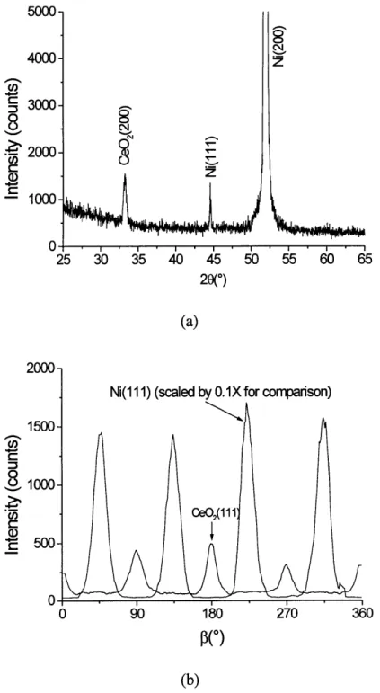
present on the substrate prior to deposition. There is only (200) oriented ceria present, as indicated by the 0/20 pattern in figure 3.1 (a). The film is epitaxial to the nickel substrate with a 450 rotation in the plane of the substrate, as shown in the beta scan of the CeO2
(111) and Ni (111) poles depicted in figure 3.1 (b). The full width at half maximum (FWHM) for the CeO2 film (- 16) is comparable to that of the underlying nickel substrate (~1 8).
Deposition from oxide on nickel
Initial attempts to deposit CeO2 from a CeO2 source directly on nickel by electron beam evaporation were unsuccessful. Such depositions yielded (111) wire texture ceria with no in plane orientation, as indicated in figure 3.2 (a). Figure 3.2 (b) shows a 200 beta scan at 20=33.080, x=3 5 0 from the plane of the substrate. This film was deposited at 1.0 A/s in an atmosphere of forming gas (Ar/5%H2). The flow rate of the gas was 5.0 sccm.
5000 4000 -S3000 8
2
2000 --1000 25 30 35 40 45 50 55 60 65 20(o) (a)2000-Ni(111) (scaled by 0.1X for comparison) 1500 8 1000 • c CeO2(111 . 500 0 90 180 270 360
R(o)
(b)Figure 3.1. Diffraction patterns of a CeO2 film deposited on nickel from a cerium metal source. A 0/20 pattern is shown in (a). The (111)
P
scans of the nickel substrate and epitaxial CeO2film are shown in (b).5000 4000 3000 2000 1000.
20(")
r, r ~ u> r a, r 200- 150- 100- 50-0 50 100 150 200 250 300 350 (b)Figure 3.2. 0/20 diffraction pattern for a CeO2 film deposited on a nickel substrate from a CeO2source (a). Shown in (b) is the (200) P scan of the CeO2film.
Prior to deposition, the substrate was heated to 6500C in approximately 1 mm Hg forming gas for 5 minutes to remove any NiO scale present on the substrate. Such a purge was
sufficient to produce epitaxial deposits of CeO2 by reactive evaporation of cerium metal on nickel. Note, however, that NiO has formed on the substrate at some point during the
deposition (as indicated by the 0/20 scan). Deposition on oxides
Deposition of CeO2 on LaAlO3 substrates typically produced epitaxial films regardless of deposition source. Figures 3.3 and 3.4 show results from films deposited on
LaAlO3 substrates during the same depositions as described above (on nickel substrates). By comparing samples from the same deposition, any variation in chamber conditions from one run to the next is eliminated. As the X-ray scans indicate, films from both the cerium metal and CeO2 source depositions were epitaxial to the single crystal LaAlO3 substrates.
Reproducibility issues Epitaxial Reproducibility
While nearly all CeO2 source depositions demonstrated the same epitaxy, independent of process conditions, the cerium metal source depositions showed
considerable variability from one run to the next. For example, three runs on single crystal nickel substrates, processed under the same temperature, deposition rate, and gas flow gave three completely different results, as indicated in figure 3.5. One film demonstrates (200) epitaxy, the second exhibits (111) wire texture, and the third cerium deposit appears to
15 0 0 0- 12000-C,
8
t-r' u, 9000- 6000- 3000- 7000- 6000- 5000- 4000- 3000- 2000- 1000-( 5J 30 35 40 45 20(0) 180P(°)
S' 5 ' 6 ' 65 270 360 (b)Figure 3.3. Diffraction patterns of a CeO2 film deposited on LaAlO3 from a cerium metal source. Depicted in (a) is a 0/20 scan, while (b) shows the (111) CeO2 3 scan.
15000 12000 9000 6000 3000 25 30 35 40 45 50 55 60 65 20(°) 30000. 25000. 4 20000. 815000ooo c 10000. 5000-200
P(O)
(b)Figure 3.4. Diffraction patterns of a CeO2 film deposited on LaAlO3 from a CeO2 source. The 0/20 scan is shown in (a). The (111) CeO2P scan is shown in (b).
O
10000-8000
6000
W
K,)a)
-2000-
2
0
25
30
35
40
45
50
55
60
65
20(0)
Figure 3.5 The 0/20 scans shown demonstrate the lack of reproducibility in CeO2 films deposited by reactive evaporation of cerium metal on single crystal nickel substrates. All three films were processed under the same conditions (1 A/s, 6500C ,1-2 sccm Ar/5%H
2). The resulting films demonstrated (200) epitaxial alignment, (111) wire texture, and
have alloyed with the substrate rather than reacting with ambient oxygen to form CeO2. A series of depositions designed to test the effect of oxygen content in the background gas composition during deposition revealed that the highest and lowest oxygen partial pressure depositions (Ar/8%0 2 and Ar/5%H2, respectively) produced epitaxial films on LaAlO3, whereas a mix of the two gases (0.7 sccm Ar/5%H2 + 0.3 sccm Ar/8%02) yielded a mixed (200)/(111) oriented CeO2 film. These results are shown in figure 3.6. It is difficult to explain these results unless some critical process parameter is not well controlled from one deposition to the next.
Sources of variation
Parameters which can be controlled during a deposition include temperature, deposition rate, angle of incoming deposition flux relative to the substrate, background pressure and background gas composition. The reproducibility of deposition temperature, rate, and angle of incoming flux are all fixed within a rather small margin of error. The background pressure during deposition is fixed within an order of magnitude. Errors are introduced in that one set of gas correction values for the ionization gauge are used for the mix of gasses in the chamber (Ar, O2, H2, etc). A drift in the value read by the ion gauge has also been noticed after measuring pressure for an extended duration in forming gas, indicating some degradation of the gauge itself. Thus, the measured background pressure during deposition is subject to some variability. This should not effect the resulting film, however, since the same gas flows are used from one deposition to the next. The pressure that results when 1 sccm Ar/5%H2 is flowed into the system may not always read the same value, but the flow into the chamber is the same.
40000-
35000-Ar/5%H
230000-S25000
-20000
=
c20000
Ar/5%H
2+ Ar/8%0
2"
15000-t
10000
-5000-
Ar/5%O
20-25
30
35
40
45
50
55
60
65
20(0)
Figure 3.6. The 0/20 scans of CeO2 films on LaA1O3 substrates demonstrate a lack of
reproducibility of epitaxy when depositing from a cerium metal source. Oxygen content of the background gas increases from the top scan to the bottom scan, yet only the film
processed in a gas composition of intermediate oxygen partial pressure exhibits a polycrystalline component.
This leaves the gas composition in the chamber as a source of variability. The chamber used during these studies does not utilize a loadlock and is, therefore, vented to atmosphere every time a new sample is loaded. This provides ample opportunity for water vapor, oxygen, and other atmospheric contaminants to adsorb to the chamber walls. The chamber is then pumped down to a base pressure of at most 2.5x107 mm Hg before beginning a deposition. It is possible that the walls are still contaminated at this point. As the chamber walls are radiatively heated by the electron gun, these contaminants desorb into the chamber. The result is a gradual change in background gas composition during deposition.
Experimental evidence for the variation of background gas composition
Depositions to different thicknesses of material supported this notion. It was found that while thin films deposited at 6500C in a mix of 0.7 sccm Ar/5%H2 and 0.3 seem Ar/8%0 2 at 0.5 A/s from a cerium metal source were epitaxial to the underlying nickel substrate, the epitaxial relationship was lost as film thickness was increased. This effect is shown in figure 3.7. The same is not true of films deposited from a CeO2 source. Figure 3.8 indicates that as film thickness deposited from a CeO2 source increases, epitaxy is maintained. These depositions were performed at 6000C and 1.0 A/s in an ambient atmosphere (no gas flowing into the chamber). The result points to one of two
conclusions. Either the change in background gas composition does not have the same effect on an oxide source deposition as it does on a metal source deposition, or the change in background gas composition itself is linked to the choice of source material. Multiple depositions from a cerium metal source were performed over extended periods without
10000
C 6000-4
O2000
A
4000
-cn-
2000-25
30
35
40
45
50
55
60
65
20(o)
Figure 3.7. CeO2 films deposited on nickel substrates from a cerium metal source undergo epitaxial growth at low film thickness, but lose this epitaxial relationship as film thickness increases, as indicated by X-ray 0/20 diffraction patterns.
100000-1000 A
80000
5000
A
:
60000
i
40000
a:)
C
00"25
30
35
40
45
50
55
60
65
28(o)
Figure 3.8. CeO2 films deposited from a CeO2 source maintain an epitaxial relationship to the substrate, independent of film thickness, as indicated by X-ray 0/20 patterns. The films were deposited on nickel substrates capped with a thin epitaxial layer of CeO2 deposited
venting the chamber in order to further investigate this apparent change of gas composition with time. A film was deposited as soon as the electron gun source had been conditioned, then the slot configuration sample shutter was closed but evaporation continued. A second substrate was exposed to the same deposition flux at a later time. The results of one such
series are shown in figure 3.9. The first deposition produced epitaxial CeO2, whereas the second film, deposited after a total of three hours of evaporation, exhibited evidence of alloy formation between cerium and nickel. This is strong evidence that the gas
composition in the chamber changes as deposition continues. There was initially sufficient oxygen present to oxidize the cerium source deposition flux and form cerium oxide. There was insufficient oxygen present in the background gas to produce CeO2 after three hours of deposition from the cerium metal source. Cerium metal was the deposited species after three hours of deposition.
It is worth noting that deposition of a metallic species can be observed after a long period of time. The metallic species begins to mirror the surfaces of the chamber walls when there is no longer sufficient oxygen in the chamber to oxidize the cerium being deposited. This mirroring results in a marked change of the appearance of the inside of the chamber from a rather dull, light tone to dark, reflective surfaces.
Film thickness calculations
Actual film thicknesses were calculated using the method of Swanepoel described earlier. Optical thicknesses were calculated for films with monitor thickness values of 2500, 5000, 7500, and 10,000 A. The range of interest for the films deposited in this study
Deposition st
immediately
source condi
arted
after
tioning
O 0Deposition started
zafter three hours
of evaporation
25
30
35
40
45
50
55
60
65
20(
°
)
Figure 3.9. X-ray 0/20 patterns for two films deposited on nickel from a cerium metal source. The first film was deposited immediately after the cerium source was conditioned, while the second film was deposited after three hours of evaporation. The first film
exhibits (200) epitaxial CeO2, while the second shows evidence of alloying between the cerium metal and nickel substrate.
5000
4000
3000
2000
1000
C) t-C' U)is outside the range for which Swanepoel's method is effective. It was necessary to extrapolate an approximate correction factor for the very thin (250 A on the quartz crystal monitor) films deposited on nickel. The actual deposition rate when the monitor was set for 1.0 A/s was approximately 0.91 A/s, as indicated in figure 3.10.
1.00-S CL
a
an
0
0.95-
0.90-
0.85-0.80
Average dep rate
=
0.91
A/s
2000
4000
6000
8000
10000
Film thickness
(A)
Figure 3.10. The figure shows average deposition rates for CeO2 films deposited on silica glass substrates as calculated from optical thickness measurements as a function of total film thickness. The deposition rate programmed into the thickness monitor was 1.0 A/s, while the actual deposition rate achieved was 0.91 A/s.
CHAPTER 4: DISCUSSION AND TESTING OF MECHANISMS
The empirical observation that epitaxial CeO2 films can only be deposited on nickel from a metal source holds true despite the lack of reproducibility of films deposited on nickel from a cerium metal source. An explanation for this observation is required in order to gain insight to the processes occurring during deposition. Finding a solution to the reproducibility issues is very difficult without a mechanistic understanding of the deposition process.
Wetting angle mechanism
The differences from metal to oxide deposition source may be a simple result of differing wetting angles of the deposited species on the substrate. In general, the wetting angle of metals on oxides is high. If a film of oxide is deposited on a metal substrate where the wetting angle is high, the result will be a film which beads up and has a very
small amount of surface area in contact with the substrate. Figure 4.1 (a) demonstrates such a case. As a result, the film will not deposit epitaxially, but will assume whatever the lowest energy configuration for the deposited species is, independent of the underlying substrate. Depositions on silica glass have shown that (111) oriented wire texture CeO2 is the preferred orientation for a cerium metal deposition when no epitaxial relationship
between the substrate and film exists. See figure 4.2. The likelihood of epitaxy is much higher if the wetting angle is reduced to the point where the deposited species is in intimate contact with the substrate, as shown in figure 4.1 (b). It is reasonable to assume that
Film Material
Substrate
(a)Film Material
Substrate
(b)Figure 4.1. Surface contact area of a film deposited on a flat substrate varies as a function of the wetting angle ( ) of the deposited species on the substrate material. For high wetting angles, as depicted in (a), there is very little substrate contact, hindering epitaxial
growth. For low wetting angles (b), substrate contact area is much higher, making epitaxial growth more probable.
5000-4000 C2 - 3000 2000--1000 5 0
25 3o 35 4o
20(0) 100- 75- 50- 25-0 50 160 150 200 P(O) 250 360 350 (b)Figure 4.2. CeO2 film deposited on a glass substrate by reactive evaporation of cerium metal. The favored alignment when no epitaxial relationship with the substrate exists is (111) wire texture, as indicated by the 0/20 scan (a) and (200) 13 scan (b) shown.
C)
8
r
epitaxial deposition of a metallic species on a metallic substrate would be more likely than epitaxial deposition of an oxide species on a metallic substrate, since homogeneous
systems (metal on metal) generally wet one another more easily than heterogeneous systems (oxide on metal).
Reduced CeO2 deposition
An attempt to significantly reduce the CeO2 oxide source prior to deposition of a film on a nickel substrate was undertaken. The wetting angle theory suggests that if it were possible to reduce the CeO2 to a metallic species, enhanced film/substrate contact would result, favoring epitaxial growth. The source was conditioned in forming gas to reduce it as much as possible prior to deposition. Substrates were covered with the sample shutter during this reduction step. Note that the oxide source darkens when heated under the electron beam, indicating an oxygen off-stoichiometry. Heating in a reducing atmosphere results in greater reduction of the source than heating in ambient. The electron gun crucible was rotated to cerium metal (without breaking vacuum) after reducing the oxide source material. The cerium source was then conditioned and used to getter any oxygen and/or water vapor from the chamber walls. Again, the substrates were covered during this conditioning. The crucible was rotated back to the CeO2 source without breaking vacuum once metallic deposition from the cerium source was visually observed (as previously described), and a film was deposited from the reduced CeO2 source on a deformation textured nickel substrate.
The results of the deposition described above are shown in figure 4.3. The film exhibits (200) biaxial alignment comparable to that of the substrate. The argument that
5000 4000 3000- 2 - 2000 -- 1000 25 30 35 40 45 50 55 60 65
(a)
600 500 400-8 300 c 200 100 0-0 50 100 150 200 250 300 350 (b)Figure 4.3. X-ray 0/20 and (111) P scans of a CeO2 film deposited from a CeO2 source on a nickel substrate ((a) and (b), respectively). The CeO2 source was conditioned in forming gas, then excess oxygen in the chamber was removed using cerium metal as a getter prior to deposition from the pre-conditioned CeO2 source. The diffraction data indicate that the film grew epitaxially on the nickel substrate.
wetting angle is controlling the epitaxy of the resulting film is supported, provided that the species deposited was actually a metallic species. It is necessary, however to verify that the species being deposited is metallic.
Thermodynamics of reduced CeO2 deposition
Figure 4.4 shows an Ellingham diagram for the NiO and CeO2 systems.44,45
According to this diagram, a PH2/PH20 ratio of 1014 would be required for metallic cerium to be the thermodynamically stable species during deposition at 6500C. Given that the
forming gas flowing into the chamber consists of 5%H2 and approximately 5ppm
impurities in the form of water or oxygen, the resulting PH2/PH2o ratio is approximately 104, well below that required to stabilize the metallic species. It seems doubtful that reduction in forming gas could have provided a metallic species for deposition. Nonetheless, the values on the Ellingham diagram are equilibrium values, and it is possible that a non equilibrium phase reaches the substrate. The source itself is at extremely high temperature, potentially hot enough to allow reduction to a metallic phase. Experimental verification of the nature of the species being deposited is required.
Electrical characterization
A system was devised to obtain an order-of-magnitude estimate of the in-situ conductivity of the samples during deposition in order to experimentally test the nature of the species being deposited. Although off-stoichiometric cerium oxide conducts at high temperatures, the metallic conductivity of cerium metal is orders of magnitude higher than that of conductive ceria. This conductivity difference between metal and oxide was used to
Temperature (oC) LOOK 140 160 180 200 400 600 PH2 PH20
Figure 4.4. Ellingham diagram for NiO and CeO2. The stability of these oxides as a function of temperature and gas composition may be read from the diagram.44,45
-20 -40 -60 -80 100 -AGO (kcal) -200 -220 -240 -260 -280
-determine whether or not the film deposited was metallic or an oxide of cerium (CeO,
Ce20 3, CeO2).
Experimental setup
Grooves were cut into silica glass substrates , allowing a fine copper wire to be attached to the ends of the substrate. Silver paste was then applied to this wire and an electrical contact pad was created at each end of the substrate. The substrate was then pasted to a stainless steel block as previously described. The wires were attached in such a way that the electrical contact pads were isolated from the sample mounting block. See figure 4.5 (a) for a diagram of the substrate setup used. A second substrate was suspended from the electrical contact wires approximately two inches from the substrate heater. This allowed concurrent collection and comparison of data from both a heated and non-heated
sample.
The electrical response of the samples was measured using a circuit as diagrammed in figure 4.5 (b). A DC transformer was used as the power supply. Paper chart recorders served to measure the voltage drop across one of two 560 resistors in series with the heated and ambient samples, respectively. Voltage was measured across a resistor in series with the sample rather than across the sample itself so that prior to deposition the measured voltage would be zero. The voltage measured prior to deposition would have been the
applied voltage had the voltage been measured across the samples, making detection of small voltage changes difficult. The applied voltage was approximately 11VDC, such that the current in the circuit was limited to <400mA if both samples shorted simultaneously.
Ag
Ag
)aste
paste
O
Copper wire
(a)
(b)
Figure 4.5. A schematic of the substrate geometry (a) and electrical circuit (b) used to perform in-situ conductivity measurements of films during deposition.
Control depositions
Control depositions were performed in order to gauge the effectiveness of the
in-situ conductivity setup prior to depositions under conditions of interest. A 1000
A
thickfilm was deposited from cerium metal in 5 sccm forming gas after a long purge (metallic deposition). The voltage drop across the control resistors for both the sample heated to
6500C and for the ambient sample (approximately 200+20'C) are shown in figure 4.6.
This voltage is directly proportional to the conductivity of the sample. Conductivity of the ambient sample increased as soon as the sample shutter was opened and deposition began. A nearly linear rise in conductivity for the sample was observed until deposition stopped, then the highly conductive film oxidized, as indicated by the abrupt drop in conductivity. The response is a combination of an increase in conduction due to increased film thickness and a decrease due to oxidation of the film material. The rise in conductivity is not
perfectly linear with increased film thickness since the film partially oxidizes as deposition proceeds. CeO2 and Ce20 3 are very stable species, and therefore will react with even
minute amounts of oxygen from the background deposition gas. The heated sample exhibits a delay in response (the conductivity does not increase as soon as the shutter is opened). The film deposited on this heated substrate was more reactive than the ambient sample. The film may have reacted more readily with atmospheric oxygen or even with the silica substrate itself as a result. CeO2 is considerably more stable than SiO2, therefore, cerium metal is capable of reacting with oxygen from the silica substrate. The delay in response exhibited by the heated film is most likely a result of film oxidation during deposition, no matter the source of oxygen. Likewise, the maximum conductivity of the
-o-
Heated
-e-
Ambient (~200')
Deposition
stopped
Ar/5%H
2off
Ar/8%O
2on
S " *-*-*0 10 20 30 40 50 60 70 80 90
Time (min)
Figure 4.6. Voltage response of films deposited from cerium metal after a long cerium metal purge of the chamber. 1000A of material was deposited in 5 sccm forming gas.
4-
3-
2-
1-a)
9
I(6500C)
100110120130
heated sample is less than that of the cold sample. Here, the increase in conductivity as a result of additional material deposition is balanced by the decrease due to oxidation of the film. Perhaps most importantly, note that the magnitude of the voltage response for these metallic depositions was on the order of a few volts. Figure 4.7 shows the electrical response of a 1000
A
thick film deposited from a CeO2 source in ambient atmosphere. During deposition, no change in conductivity is observed for either the heated or ambientsample. The material being deposited is an insulator. Prior to deposition, the sample was an open circuit, resulting in no voltage drop across the resistor. This did not change as material was deposited. Only when deposition stopped did the conductivity of the heated sample begin to rise. This indicates that while the film was being deposited, it was very close to being fully oxidized. The primary source of oxygen in the chamber (that is, oxygen evolved from the CeO2 source itself) was removed when deposition was stopped, and the heated film began to reduce. The cold sample did not demonstrate this behavior since at 2000C, conductivity of the sample (whether it is reduced or not) is too low to observe. Appendix B shows a calculation of the amount of oxygen evolved from the source per unit time. A cosine distribution of evaporated flux from the source material is assumed. This allows calculation of the total amount of material evaporated into the chamber per unit time. The evaporant is assumed to undergo a reduction from
stoichiometric CeO2 to CeO1.9 upon evaporation from the source material. This liberates an equivalent flow of 0.13 sccm of pure 02 into the chamber as a result of CeO2 evaporation. This represents more than five times the flow of oxygen introduced to the background pressure during a reactive evaporation of cerium metal (0.30 sccm Ar/8%O2).
-o--Heated
(650'C)
-*-Amhient (1N°qni m0--O_-0OO 0 /o
Heater off
o
)osition
o)ped
o 0 0 0 0 / 0/
o
0 0 O0.25-
0.20-
0.15-
0.10-
0.05-
0.00--0.05-
I
30
40
5
060
70
80
90
Time (min)
Figure 4.7. Voltage response of films deposited from CeO2 in ambient atmosphere (no gas flowing).
20
Dep
stol
O
10
S .. . ... ... . .- I - m - n - m - m - m --- m -- m -- --m vWV
%a - W f WOxygen evolution from the source material is likely the most significant source of oxygen in the background chamber pressure during a CeO2 evaporation. Note that when the run was complete and the hot sample was allowed to cool, its conductivity dropped to an unobservable level. Also, note that the magnitude of the response from this CeO2
deposition was several orders of magnitude lower than the response demonstrated by a metallic film (less than 1 millivolt vs. several volts)
Electrical response during epitaxial depositions from cerium
Figure 4.8 shows the response of a film deposited from a cerium metal source in conditions which normally produce an epitaxial CeO2 film on nickel. Total film thickness was 1000
A,
and the background gas composition was 0.7 seem Ar/5%H2 + 0.3 seem Ar/8%O2. Here, a reduced species was deposited, as indicated by the immediate increase in conductivity observed when deposition started. Note that the cold sample showed no response, despite the fact that the response of the hot sample indicates that a reduced species was deposited. This is again due to the fact that at low temperatures, theconductivity of CeO2 (whether reduced or not) is too small to observe. The incoming flux of reduced material was halted when deposition was stopped by closing the sample shutter. An abrupt decrease in the conductivity of the film was observed as the film oxidized. Another drop in conductivity is evident corresponding to the time the electron gun was shut off. Cerium vapor serves to getter any oxygen from the system. When the electron gun was shut off, the atmosphere in the chamber became more oxidizing. The film began to oxidize at a higher rate, resulting in a decrease in conductivity. The final drop in conductivity corresponds to the cooling of the sample. Note that the magnitude of the
C9
-- o-Heated
(6500C)
c
-e--Ambient
(~200
°)
0
o
\
/
o
Deposition stopped
/
o(dosed
sample
shutter)
0
o
o
0 0
S
e
gun off
Heater off
o 0--- -0 --- 0 -0-- ---
-0-0----0-4
6
I '
' I
3I
0 10 20 30
I40
I
0
I
I I
40 50 60 70 80 90
Time (min)
Figure 4.8. Voltage response of films deposited from cerium metal in a background gas composition consisting of 0.7 sccm Ar/5%H2+ 0.3 sccm Ar/8%02.


![[PDF] Cours informatique Initiation Android | Formation informatique](data:image/gif;base64,R0lGODlhAQABAIAAAP///wAAACH5BAEAAAAALAAAAAABAAEAAAICRAEAOw==)