Design and Fabrication of micro- and
nano-dielectric structures for imaging and focusing at
optical frequencies
by
Satoshi Takahashi
M.S., Mechanical Engineering (2006)
Massachusetts Institute of Technology
MASSACHUSETTS INSTiJTE OF TECHNOLOGY
JUL 2 9 2011
LIBRARIES
ARCHIVES
Submitted to the Department of Mechanical Engineering
in partial fulfillment of the requirements for the degree of
Doctor of Philosophy in Mechanical Engineering
at the
MASSACHUSETTS INSTITUTE OF TECHNOLOGY
June 2011
@
Massachusetts Institute of Technology 2011.
Author .
Certified by..
All rights reserved.
Department of Mechanical Engineering
February 15, 2011
...
George Barbastathis
Professor of Mechanical Engineering
Thesis Supervisor
A ccepted by ...
...
..
. .. .
David E. Hardt
Chairman, Department Committee on Graduate Students
e_
.. . . % .. .. . . . . . . . . . . . . . . . . . . . . . . . . . .
. .
I.
Design and Fabrication of micro- and nano- dielectric
structures for imaging and focusing at optical frequencies
by
Satoshi Takahashi
Submitted to the Department of Mechanical Engineering on February 20, 2011, in partial fulfillment of the
requirements for the degree of
Doctor of Philosophy in Mechanical Engineering
Abstract
In this thesis work, design and fabrication of micro- and nano-photonic structures both in the diffraction regime and sub-wavelength regime have been investigated.
In the diffraction regime, two types of optical systems and optical elements were investigated for application in LCD manufacturing. With the increasing demand for larger LCD screens at lower cost, technology for low-cost high-throughput manufac-turing systems, as well as efficient repair systems within the manufacmanufac-turing line for any manufacturing defects, are crucial for manufacturers. The first system investi-gated in this work is a novel optical lithography system for LCD manufacture using a computer generated hologram (CGH). The fabrication challenges for a highly com-plex pattern inherent in CGHs are addressed. The second system is a defect repair system utilizing a blazed grating matrix (BGM). The BGM generates multiple high intensity spots from a high-power pico-second pulsed laser, controlled by a spatial light modulator, which can ablate the surface of the substrate to eliminate residues and excess material. In both systems, high efficiency and pattern fidelity are required for the optical element, and micro- and nano-fabrication techniques were used in order to achieve the required specifications.
In the sub-wavelength regime, locally periodic dielectric photonic structures with adiabatic variation were designed and verified, with application in lensing in optical
frequencies. Structures such as rod lenses and Luneburg lenses are investigated.
Especially the latter type of lenses have been conventionally difficult to implement in optical frequencies due to its specific refractive index profile. With the high flexibility
of gradient effective index design with the " aperiodic" dielectric nanostructures, along
with the design method using Hamiltonian Optics investigated in this research, the
Luneburg lens was designed, fabricated, and verified at the wavelength of A = 1.55pim.
Thesis Supervisor: George Barbastathis Title: Professor of Mechanical Engineering
Thesis Reader: Gang Chen
Title: Professor, Mechanical Engineering Thesis Reader: Steven G. Johnson Title: Professor, Mathematics
Acknowledgments
"KJ-in Yano Gotoshi", equivalent of "time flies" in Japanese, literally means light (i.e. sun; daytime) and shadow (i.e. moon; nighttime) is like a flying arrow.
Indeed, the time I spent at MIT as a graduate student flew past as if at the speed of light. And as is discussed in this thesis, the propagation of light and a flying arrow have much in common. Along this trajectory, I was very fortunate to meet, discuss, and be advised by many great people, without whose help the work presented here could not have been accomplished. I realize that there is no way I can do justice to the people that I am appreciative of, nor a way I can appreciate all of the people that
I must, but I hope these acknowledgements will do their best in conveying my sincere
appreciation.
First and foremost, I owe tremendous amounts of gratitude to my advisor, Prof. George Barbastathis. His insightful and critical thinking have influence me greatly and his comments have always aided my research path.
Also, I would like to thank my thesis committee members, Professor Gang Chen and Professor Steven G. Johnson. Discussion with them have always been inspiring and set paths for this research from different perspectives. Prof. Chen's insight into nanostructures and Prof. Johnson's deep knowledge and experience vitalized my research every meeting I had with them. I am greatly honored to have such a prestigious Committee for my research.
I also would like to thank my collaborators of the work I have done, particularly Pepe Dominguez-Caballero, James Sungjin Lee, Si Ho Seoung, Chihhao Chang, Se Young Yang, and Johnny Choi. They are great researchers, and I learned
tremen-dously through working and discussing with them.
My labmates in the 3D Optical Systems Lab, both old and new, had always been
great to turn to both professionally and for fun. They have made my lab life invaluable and hard to leave from. I have always appreciated their company.
I was very fortunate to meet a lot of great people outside of lab as well, either
but in terms of helping me through great advices for research, I would like to give my gratitude to Eiji Iwase and Haruka Tanji. Some of the results presented here would not have been produced without their valuable input.
The Microsystems Technology Lab (MTL) and the Nanostructures Laboratory
(NSL), at MIT, as well as the Center for Nanoscale Systems (CNS) at Harvard were
great facilities to work in with great staff maintaining the environment and the ma-chines. Especially Vicky Diadiuk, Kurt Broderick, Jim Daley, and JD Deng were of tremendous help in fabricating devices and conducting experiments.
I would also like to thank my funding sources, Samsung Electronics, centre for
environmental sensing and modeling (CENSAM) from the Singapore-MIT alliance, and the Institute of Soldier Nanotechnology (ISN).
Lastly, I cannot end this acknowledgement without mentioning my parents and brothers for supporting me all the way through my career here at MIT. Although living very far, I always felt safe and supported thanks to their warmth.
Contents
1 Introduction 19
1.1 Diffractive Optics . . . . 19
1.1.1 Computer Generated Holograms . . . . 20
1.1.2 Fabrication of Diffractive Optical Elements . . . . 20
1.2 Sub-wavelength Optics . . . . 20
1.2.1 Periodic Subwavelength Structures . . . . 21
1.2.2 Non-periodic Subwavelength Structures . . . . 21
1.2.3 Hamiltonian Optics . . . . 22
1.2.4 Fabrication of Sub-wavelength Structures . . . . 25
1.3 Thesis Objective and Contributions . . . . 26
1.3.1 Outline of Thesis . . . . 26
2 Diffractive Optics for LCD manufacture and repair 29 2.1 LCD Lithography Using CGH . . . . 29
2.1.1 Design of the Optical System . . . . 30
2.1.2 Fabrication of the CGH . . . . 31
2.1.3 Optical Characterization . . . . 39
2.1.4 Exposure Test . . . . 41
2.1.5 Conclusion . . . . 43
2.2 Multi-spot Ablation System for LCD Pixel Repair Using a Blazed Grat-ing M atrix . . . . 43
2.2.1 Design of the Optical System . . . . 44
2.2.3
2.2.4
2.2.5 2.2.6 2.2.7
Blazed Grating Matrix . . . . Analysis of Fabrication Parameters and Tolerance
Fabrication of the Grating Matrix . . . . Experimental Results . . . . Conclusion . . . .
3 Sub-wavelength Optics for Imaging
3.1 Hamiltonian Optics . . . . 3.1.1 Hamiltonian Optics for Sub-wavelength Structures .
3.1.2 Phase Space Representation . . . .
3.2 Design of GRIN Rod Structures . . . . 3.2.1 Phase Space Representation . . . .
3.3 Design and Fabrication of Luneburg Structures . . . . 3.3.1 Luneburg Lens . . . .
3.3.2 Design of Aperiodic Luneburg Lens . . . .
3.3.3 Fabrication . . . .
3.3.4 Experiment and Results . . . .
4 Conclusion and Future Work 4.1 Future Work . . . .
4.1.1 CGH Lithography...
4.1.2 Multispot Ablation . .
4.1.3 Aperiodic Nanostructures
A Fabrication Processes
A.1 Fabrication Process of the Computer Generated Hologram . . . . . A.2 Fabrication Process of the Blazed Grating Matrix . . . . A.3 Fabrication Process of the Aperiodic Nanostructures . . . .
. . . . 54 . 55 . . . . 58 . . . . 63 . . . . 69 107 . . . . 107 . . . . 108 . . . . 108 . . . . 108 111 111 112 112
List of Figures
1.2.1 Dispersion diagram of a square lattice of silicon rods. . . . . 22
1.2.2 Dispersion surface of a square lattice of silicon rods. . . . . 23
2.1.1 Optimized binary phase in-line CGH that reconstructs the MIT logo. 31
2.1.2 Optimized binary phase in-line CGH that reconstructs a grating matrix. 32
2.1.3 Fabrication method for the CGH using HSQ and e-beam lithography. 32
2.1.4 Dose Matrix to determine the proper dose for the CGH. . . . . 34
2.1.5 SEM image of the fabricated CGH with design shown in Figure 2.1.1 35 2.1.6 Comparison of fabricated CGHs with (a) over- and (b) under-exposure. 35 2.1.7 Design of in-line CGH optimized using the simulated optical diffuser
initial guess. . . . . 36
2.1.8 SEM image of the fabricated CGH with design shown in Figure 2.1.7 37 2.1.9 SEM image of the fabricated CGH with design shown in Figure 2.1.7 38 2.1.1 (Comparison of fabricated CGHs with design for the same section. . . 39 2.1.1SEM image of fabricated CGH for grating matrix. . . . . 40 2.1.1'2omparison of various dose conditions at various sections of the
pat-tern. Note that while 1.25pC/cm2 (left side) is a better dose for the
features in the top row, the features in the bottom row require a dose
of 80pC/cm2 (right side). . . . . 41
2.1.13lock diagram of CGH evaluation algorithm. . . . . 41
2.1.lExample confocal microscope data of the reflection grating CGH. . . 42
2.1.1TExample of binarized and stitched data: (left) desired CGH; (right)
2.1.1(Epectral cross-correlation method. . . . . 43
2.1.1 Example of cross-correlation map. . . . . 44
2.1.183rror Map of the best fabricated reflection grating. . . . . 45
2.1.19The designed reconstructed intensity (left) and the numerically recon-structed intensity of the fabricated CGH. . . . . 46
2.1.2(Comparison of designed and fabricated CGH patterns. (a) desired CGH pattern; (b) fabricated CGH pattern . . . . 47
2.1.2Schematic of optical characterization setup. . . . . 47
2.1.2 Reconstructed intensity distribution by fabricated in-line CGH . . . . 48
2.1.23Donfocal microscope image of experimentally printed pattern on pho-toresist (left) and numerically reconstructed intensity of the reflection grating CGH used in the experiment. . . . . 48
2.2.1 Schematic of the optical setup for laser ablation system . . . . 49
2.2.2 Optical setup of the SLM at approximately 45 degrees. . . . . 50
2.2.3 Schematic of optical setup and measured maximum power at each posi-tion along the beam path. Details of the optical setup will be discussed in Section 5. . . . . 51
2.2.4 Schematic of the geometry of the main imaging section with relay optics and gratings to be optimized. . . . . 52
2.2.5 Specifications of Mitutoyo M Plan Apo NUV 100X ??. . . . . 53
2.2.6 Desired grid at the image plane. . . . . 53
2.2.7 Schematic of the blazed grating. . . . . 56
2.2.8 Design of the grating matrix. The blazed gratings are denoted as stripes, and not to scale. The grating in the red box (at the corner of the matrix) has the smallest pitch of 1.17pum when MA = 1, m = 1, and the grating in the blue box (next to the center) has the largest pitch of 23.7m for the same conditions. . . . . 57
2.2.9 Simulated transmitted efficiency as a function of the number of steps for stair-case blazed gratings. . . . -. . . . 58
2.2. 1Schematic of the analyzed angle tolerances. 0 is the angle of the vertical
plane, and A4 is the angle error of the inclined plane. . . . . 59
2.2.1IFDTD simulation setup for blazed grating fabrication tolerance
anal-ysis. Notice that discrete steps and edge-rounding was taken into
ac-count in the simulation. . . . . 59
2.2.lEfficiency variation with fabrication errors in vertical surface and
di-agonal surface for 1.617m pitch grating (closest to corner). ... 61
2.2.13Efficiency variation with fabrication errors in vertical surface and
di-agonal surface for 2.98m pitch grating. . . . . 62
2.2.14Efficiency variation with fabrication errors in vertical surface and
di-agonal surface for 23.67mm pitch grating (closest to center). ... 63
2.2.1,Wabrication process for blazed grating array with a grayscale mask. 63
2.2. 1(Relationship between transparency and profile height of the developed photoresist (a) and between the optical density and profile height of the developed photoresist (b) for optimized fabrication process parameters, obtained experimentally. (b) was obtained from (a) and equation 2.2.9. In both figures, red line shows the profile with 2 sec exposure with contact lithography, and the green line shows the profile with 3sec
exposure. ... ... 64
2.2.1iProfile of the fabricated blazed gratings with 10pm pitch. . . . . 65
2.2.1drocess for nanoimprint lithography using HSQ. . . . . 65
2.2.196chematic of the optical setup for single-spot ablation experiment. . . 66
2.2.26BEM images and AFM measurements for experiment 1 (c.f. Table 2.2.5). 67
2.2.2SEM images and AFM measurements for experiment 2 (c.f. Table 2.2.5). 68 2.2.2SEM images and AFM measurements for experiment 3 (c.f. Table 2.2.5). 68 2.2.2SEM images and AFM measurements for experiment 4 (c.f. Table 2.2.5). 69 2.2.2(a) Design of the binary grating matrix. (b) Optical micrograph of the
grating structure. . . . . 70
2.2.24a) Schematic and (b) Photograph of optical setup for multi-spot
2.2.2GVulti-spot image at substrate plane, corresponding to the grating ma-trix as shown in Figure 2.2.24. The distance between the spots was approximately 29pm (designed for 30pm). Aberration for some spots
can be observed due to fabrication and alignment errors. . . . . 71
2.2.2TPatterns of spots at the substrate plane generated by controlling the
SLM. SLM configuration for the checkerboard (a) and the image of the
spots at the substrate plane (b). . . . . 71
2.2.28?atterns of spots at the substrate plane generated by controlling the
SLM. SLM configuration for the horizontal stripes (a) and the image
of the spots at the substrate plane (b). . . . . 72
2.2.2Tatterns of spots at the substrate plane generated by controlling the
SLM. SLM configuration for vertical stripes (a) and the image of the
spots at the substrate plane (b). . . . . 72
2.2.3(Intensity at the substrate plane from the multi-spot experiment with the blazed grating matrix. Aberration can be seen at the spots which
are due to misalignment of the optics in the setup . . . . 73
3.1.1 Schematic diagram of a lattice with (a) varying lateral spacing and (b)
varying radius). . . . . 77
3.1.2 Equi-frequency contours at various lateral lattice spacing with same
rod radius (a), and various radius with same lattice spacing (b). . . . 80
3.2.1 Hamiltonian ray tracing and FDTD results overlaid for comparison.
The solid lines show the rays, and the dashed lines show the wavefronts
obtained by calculation of optical path lengths along the rays. .... 81
3.2.2 The intensity profile from FDTD at the focal plane of Figure 3.2.1. 82 3.2.3 Comparison of RMS spot size from Hamiltonian Optics and FDTD
spot size as a function of angle. . . . . 83
3.2.4 Comparison of RMS spot size from Hamiltonian Optics and FDTD
3.2.5 Equi-frequency contours at various lateral lattice spacing with same
rod radius (a), and various radius with same lattice spacing (b). . . . 84
3.2.6 Equi-frequency contours at various lateral lattice spacing with same
rod radius (a), and various radius with same lattice spacing (b). . . . 85
3.2.7 Local index of refraction seen by each ray, corresponding to each curve,
propagating as shown in Figure 3.2.1, plotted along the radial direction. 86
3.3.1 Schematic illustration of ray propagation through a Luneburg lens. A
plane wave incident to the lens forms a focus at the opposite edge of
the lens. ... ... 87
3.3.2 Geometry of the nanostructured Luneburg lens. . . . . 88 3.3.3 Hamiltonian ray tracing results (blue lines) overlaid with FDTD
analy-sis (red and blue shading) for the Luneburg structure in Figure 1. The green dots represent equal-OPL points on each ray. It can be seen that the equal-OPL points align well with the wavefronts from the FDTD
sim ulation. . . . . 89
3.3.4 Schematic illustration of a hole structure in a silicon material. .... 89
3.3.5 First mode of the dispersion diagram for TE and TM modes in 2D rod
and hole structures for a rod/hole radii of r = 0.255. . . . . 90
3.3.6 First mode of the dispersion diagram for TE and TM modes in 2D
rod and hole structures for "complementary" rod/hole radii, where r = 0.255 for rods and r = 0.455 for holes. . . . . 91 3.3.7 Schematic illustration of "complementary" rods/holes. The hole has
a diameter which covers the maximum possible area between the rods
but does not overlap with any of the rods. . . . . 91
3.3.8 Plot of the top edge of the first mode of the dispersion diagram for
each configuration, as a function of the critical dimension. From the fabrication perspective, it is desirable for the design to be near the
3.3.9 Dispersion diagram of silicon rods in 2D (blue) and 3D (red). The green
light denotes the light line for silicon dioxide, which is underneath the structure. Only the first modes are shown for each structure. Parts of the band in the 3D case are above the dioxide light line, which denotes
a leaky mode whereas the band is completely guided in the 2D case. . 94
3.3.1CSchematic of the 3D structure that was used to solve for the dispersion
diagram . . . . 95
3.3.1Fabrication process of the aperiodic nanostructures with waveguides
for light coupling. . . . . 96
3.3.12SEM micrograph of a fabricated Luneburg structure where the
cen-ter part is attached together as opposed to the designed rods as seen outside of the Luneburg region. This is due to overdose in e-beam lithography at the center, where the structures are much denser. The
period of the lattice is 194nm. . . . . 97
3.3.13EM micrograph of a fabricated Luneburg structure with successful
dose compensation. All silicon rods are isolated from each other as opposed to what can be seen in Figure 3.3.12. The period of the lattice is 258nm, and the overall size of the nanostructure region is 50pm by 20[tm. Waveguides for coupling light into the structure can be seen on
the left and right of the structure. . . . . 98
3.3.148chematic illustration of the experimental setup for the Luneburg lens
structure using an NSOM. . . . . 100
3.3.1,Uharacteristics of the infrared detector PDF10C from ThorLabs: (a) responsivity towards wavelengths of light (b) frequency response (c)
3.3.16NSOM measurement along a waveguide leading to the Luneburg
struc-ture. (a) shows the profile measurement, the center yellow part showing the waveguide which is 320nm high from the substrate. (b) shows the intensity plot taken from the NSOM. (c) shows a plot of intensity at a cross-section, fitted with a Gaussian profile (red line). FWHM of the
Gaussian profile is 16.19 rn. . . . . 101
3.3.1Z\TSOM measurement of the Luneburg structure with A = 1.5 5pm laser
beam probed from the left hand side of the figure. The focus at the right edge of the Luneburg structure, outlined with white dotted line,
is evident. . . . . 102
3.3.18ntensity cross-section at focus of the Luneburg structure. The FWHM
is around 1 pm . . . . 103
3.3.I9SOM measurement of the Luneburg structure with A = 1.55pm laser
beam probed from the left hand side of the figure. The The focus at the right edge of the Luneburg structure, outlined with white dotted
line, is evident. . . . . 104
3.3.2(Intensity cross-section at focus of the Luneburg structure when probed
from 45 degrees. The FWHM is around 3.48 pm . . . . 105
4.1.1 Schematic illustration of a 3D Luneburg lens fabricated through stack-ing of 2D features generated by fabrication methods such as e-beam
List of Tables
2.2.1 Specifications of Mitutoyo M Plan Apo NUV 100x [11] . . . . 46
2.2.2 Specifications of the laser [4] . . . . 50
2.2.3 General system specifications . . . . 52
2.2.4 General system specifications . . . . 60
2.2.5 Power and fluences used for single-point ablation experiment . . . . . 64
3.3.1 Comparison of fabrication parameters for Luneburg lens designs in-tended for two different lattice constants. A = 1.55pm. Note that the minimum feature size (either rod diameter or gap size) is increased from 32nm to 96nm by increasing the lattice constant a. . . . . 93
A. 1. 1Fabrication Process of the CGH described in Chapter 2. The machine column refers to the machine that has been used in the Nanostructure Laboratory (NSL) at MIT unless otherwise noted. . . . .111
A.2. 1Fabrication Process of the aperiodic Luneburg lens described in Chap-ter 3. The machine column refers to the machine that has been used in the Nanostructure Laboratory (NSL) at MIT unless otherwise noted. 112 A.3. 1Fabrication Process of the blazed grating matrix described in Chapter 2. The machine column refers to the machine that has been used in the Microstructures Technology Laboratory (MTL). . . . . 113
Chapter 1
Introduction
Electromagnetic waves behave quite differently depending on the feature sizes of the structure that it impinges on compared to the wavelength of the incident wave. Opti-cal components such as phase gratings and holograms, whose feature sizes are similar but larger than the wavelength, function in the diffractive regime for imaging and spa-tial/spectral measurement. On the other hand, sub-wavelength structures, such as photonic crystals, possess functions that are not observable in the diffraction regime, bandgaps being one of the most commonly investigated among others. Both regimes provide opportunities for powerful optical functionalities, and proper design and fab-rication of the components is critical in order to obtain the optical properties intended
by the application.
1.1
Diffractive Optics
Diffraction is one of the most fundamental phenomena in classical optics, along with reflection and refraction. Diffractive optical elements (DOEs) are optical components that utilize this phenomenon for specific optical applications, such as intensity mod-ulation from one optical plane to another. The feature size of DOEs are generally in the order of the wavelength of the radiation, since this size scale is where the effect of diffraction is largest.
used in spectroscopy, and holograms, which are used in, besides art pieces, 3D infor-mation storage [56] and 3D imaging [18].
1.1.1
Computer Generated Holograms
A hologram is an optical element that can reconstruct wavefronts that have been
recorded. The original holograms, one of the first discussed by Gabor [30], require optical recording of the 3D image to be reconstructed. However, holograms can be designed numerically considering the fact that the diffractive light propagation, either in the Fresnel or Fraunhofer regime, can be expressed mathematically with Fourier Transforms. These types of holograms, called computer generated holograms (CGHs), were first proposed by Brown and Lohmann in 1966 [22], and since then have been investigated widely for beam shaping [40], optical trapping [38], optical signal processing [44], optical communications [23], and 3D displays [39].
1.1.2
Fabrication of Diffractive Optical Elements
In order to reconstruct an arbitrary pattern with a hologram precisely, in general, the ability to produce arbitrary phase and intensity at the hologram plane is required. However, this is not practical from the fabrication point of view, when the feature sizes are in the order of microns to sub-microns. Especially, since much of the es-tablished fabrication technology in this length scale, such as optical lithography, is two-dimensional, the freedom to tune the phase is limited unless highly complicated and expensive manufacturing technology is introduced, such as ones discussed in [42].
1.2
Sub-wavelength Optics
There has been large research interest in sub-wavelength photonic structures espe-cially in the past two decades. Espeespe-cially for periodic structures known as photonic crystals, investigations have shown various interesting properties.
1.2.1
Periodic Subwavelength Structures
In 1987, Yablonovich found out that these structures possess bandgaps, equivalent of electric bandgaps in crystal structures [68], and since then, various interesting phe-nomena and applications have been investigated by numerous researchers, including slow light [20], super collimation [55], negative index [26], form birefringence [29], and so on.
In any of the above applications, the properties of the periodic nanophotonic structure can be expressed by the dispersion diagram. A dispersion diagram plots the frequency of the modes of interest as a function of the wavevector k. Figure 1.2.1 shows a dispersion diagram along the edge of the Brillouin zone for TM modes in a
2D square lattice of a dielectric circle (equivalent of an infinitely long dielectric rod)
in air, shown in the inset. The red dotted lines show dispersion curves of air (n = 1),
also known as the light cone. The bandgap between the first mode and the second mode is evident, as well as the flattening of the mode near point X. Noting that the gradient of the plot of the modes in this diagram, Ow/Ok is equal to the phase velocity
vp, flattening of the mode implies slow light, and negative slope a negative index at
that frequency. Super collimation and form birefringence can be explained with a
2D dispersion diagram, where the frequency of the modes are plotted both in k, and
in ky (FIgure 1.2.2). Both utilize the highly nonlinear properties of the dispersion curves especially at high frequency regions, which are due to the periodicity of the structure [27].
1.2.2
Non-periodic Subwavelength Structures
Obviously, interesting sub-wavelength structures are not limited to periodic ones. One interesting application of non-periodic nanostructures is an optical cloak. The theory of optical cloaks was first given by Pendry [37] and Leonhardt [47], and Valen-tine fabricated a version of a cloak with nano dielectric structures using focused ion beam for 2D [41], and Ergin for 3D [64]. Note that in either cases, nanostructures are used to obtain a spatial distribution of effective index of refraction through effective
D(x,y a-Di '' air (n=1) (n=3.45) 0 .3 - ---. --- --- -- -r..-- ... - - -- -- ..-r X M r
Figure 1.2.1: Dispersion diagram of a square lattice of silicon rods.
medium theory.
1.2.3
Hamiltonian Optics
In this work, Hamiltonian Optics will be used extensively for design and optimization of nanophotonic structures. Although this method originally was used with assump-tions for a slowly varying medium, as was shown by Fan [66] and St. J. Russell [59], this method can also be utilized to trace rays in nanostructures with slowly vary-ing periodicity, which actually have high frequency non-smooth variation of actual refractive index.
In Hamiltonian Optics, the ray trajectories through a gradient index medium can be obtained through solving the set of Hamiltonian equations along with a certain initial condition in position in space and momentum (corresponding to the k-vector), which can be expressed as,
dq OH dp OH
dt p ' dt q (
where q is the geometrical position in Cartesian coordinates, p is the momentum, and H is the Hamiltonian, which is a conserved quantity along the ray trajectory.
0.5 0 . ky 0.4 0.5 0.3 0.4 0.2 0.3 0.1 0.1 0 0
Figure 1.2.2: Dispersion surface of a square lattice of silicon rods.
Foundations of Hamiltonian Optics
Fermat's Principle states that light propagates from one point to another along a minimum path length, mathematically expressed as,
L = 2n(qlds,
/P2
(1.2.2)where L is the optical path length, pi and P2 are beginning and end points, n(q is
the index of refraction at point in space with Cartesian coordinates q. In Cartesian coordinates, = (X(z), y(zZ), = I(dx)2 + (dy)2 + (dz)2 q ds (1.2.3) (1.2.4)
where z is the direction parallel to the optical axis. Substituting 1.2.3 to 1.2.2, pP2 L = n(x(z)(z), z) V( = Z2
n(x(z),y(z),z)
z+
= j n(q(z), q(z), z) 4+2+dz.
Now, we define the Lagrangian as:
Y = n(q, 4, z) |4|2 +1.
The Fermat's Principle can be described as:
L =j Y(q, 4, z)dz = min., and from Y(q+eh,4+Eh,z) =6+ eY h + og O h ,
a8
The variation in the optical path is,
CZ28 82 O
L(ch) = 2[ (q, 4, z) + j h + ' )]dz = min.
fz2 (( a
a4
6L(eh)
= Eq
h+
.
hdz
Sz2 6j:2(~
9Y
d
d&)hdza2
Therefore, in order for the path length L to have minimum path length, 82 d &2 - = 0. dx)2+ (dy)2+ (dz)2 2
+
1dz (1.2.5) (1.2.6) (1.2.7) (1.2.8) (1.2.9) (1.2.10) (1.2.11) (1.2.12) (1.2.13) (1.2.14)i.e.,
o~n
d n42 + 1 - - = 0. (1.2.15)
Og
d z .|4|2 + 1Now, the momentum and Hamiltonian are defined as,
p =4 - , (1.2.16)
H = p4 - Y. (1.2.17)
Therefore we obtain the Hamiltonian equations as, OH
-= H (1.2.18)
p = H (1.2.19)
9q
1.2.4
Fabrication of Sub-wavelength Structures
With emergence and maturity of micro- and nano-fabrication technology, photonic crystal and other nano-photonic structures have been successfully fabricated to func-tion in optical frequencies, either in 2D [50] or 3D [49].
Photonic crystals without defects can take advantage of their periodicity, either in
2D or 3D, and be fabricated with interference lithography [49] or self-assembly [67].
These techniques allows relatively fast fabrication of large-area structures. However, once defects are introduced to periodic structures, or if the structure is non-periodic, other fabrication techniques that are usually more time consuming, such as electron-beam (e-electron-beam) lithography, must be incorporated. For 3D non-periodic structures, there are several different types of fabrication methods. One is the use of either two-photon ablation or polymerization in a 3D material [45, 34], another set of technology involves the use of a well established 2D lithography technique and stacking of multiple layers in order to build up the third dimension [51, 43, 54]
1.3
Thesis Objective and Contributions
This thesis work presents design and fabrication methods for optical components whose feature sizes are close to or smaller than the wavelength of light of interest. Especially for visible frequencies, these components possess feature sizes in the order of tens of microns to hundreds of nanometers. Both diffractive and sub-wavelength regimes will be investigated, and experimental verification is conducted to prove the capabilities of the design and fabrication techniques presented.
In the diffractive regime, two novel optical systems are designed, fabricated, and tested. One is a non-contact high-resolution LCD manufacturing system using a
CGH, and the other is a multi-spot ablation system for LCD pixel repair using a
blazed grating matrix. The former system resolves the problem with conventional lithography techniques, being very expensive in order to meet high-throughput and high-resoluction requirements at the same time. The latter system can be used to repair defects in LCD displays with high speed and low cost by parallel ablation of defects using multiple spots. The diffractive optical elements for both systems were fabricated using micro-fabrication technologies and tested in an optical setup.
In the subwavelength regime, an optical device was designed and fabricated for
highly flexible lensing application in optical frequencies. Their design method
us-ing Hamiltonian Optics was established, along with fabrication of a proof-of-concept device and its verification. Although there have been reports on non-periodic nanos-tructures, not much research has been conducted to incorporate the extensive theory of photonic crystals and dispersion relations into non-periodic structures and use them as tools to design nanostructures for effective index control in optical devices such as lenses with functions that were not possible with conventional manufacturing techniques.
1.3.1
Outline of Thesis
In Chapter 1, overview of concepts and previous work regarding diffractive and sub-wavelength optics were discussed. The concept of diffraction and diffractive optical
elements have been introduced, and previous literature on analysis, design, and fabri-cation of DOEs, especially CGHs, have been discussed. Also, interaction of light with sub-wavelength structures have been discussed, both' for periodic and non-periodic structures. Hamiltonian Optics was introduced as a ray-tracing technique as well as fabrication technologies for these structures.
The remainder of this thesis is structured as follows:
Chapter 2 will discuss two optical systems using DOEs, namely, an optical lithog-raphy system using a CGH, and a multi-spot laser ablation system with a blazed grating matrix. For both systems, the system concept and overall design will be dis-cussed, as well as the specific components, especially the design and fabrication of the DOEs. The experimental results of the system will be discussed and analyzed.
In Chapter 3, sub-wavelength aperiodic structures will be discussed. The design method for these structures based on Hamiltonian Optics will be discussed in detail, and two example structures will be designed, namely, a rod lens and a Luneburg Lens. Simulation results of the designed structures using Hamiltonian Optics will be discussed, and will be compared with the finite difference in time domain (FDTD) method. Further, fabrication and experimental results of the Luneburg Lens structure will be presented.
Chapter 2
Diffractive Optics for LCD
manufacture and repair
Liquid crystal displays (LCDs) are omnipresent in our daily lives, from cell phone screens to advertisement displays. Due to high competition, it is critical to fabricate them at as low cost as possible to sell at a competitive price and gain revenue at the same time. Especially as the demand for larger LCD displays grow, it becomes more critical to use a manufacturing method that is fail-proof and fail-safe. The former can be achieved with a high-precision fabrication method, and the latter with an efficient repair system.
In this Chapter, two types of optical systems are introduced, one for LCD man-ufacturing and the other for repair within the manman-ufacturing line of the displays. In either cases, high precision and high throughput are required, while keeping the overall cost of the system and process low. The optical systems are designed using analytical and numerical methods, an experimental setup is built and tested, and the diffractive optical device was fabricated using microfabrication techniques.
2.1
LCD Lithography Using CGH
Lithography has become a crucial technology to fabricate structures with micron to sub-micron features. Among the wide variation of lithography techniques, optical
lithography, especially steppers which have high efficiency and can obtain high res-olution, have become the industry standard. While optical lithography is a very efficient fabrication method, since light propagation suffers diffraction in general, in order to replicate a high fidelity mask pattern close to the diffraction limit, either the substrate must be in close contact with the mask, or highly expensive and large optics must be used to image the mask pattern on to the substrate with minimum aberration.
In this section, a lithography system for LCD manufacturing using a computer generated hologram (CGH) will be introduced. The advantage of this system is that it is non-contact, hence high-throughput while allowing for diffraction-limited pattern generation on the mask without using expensive and massive optics.
CGH lithography has been proposed and investigated in the past. However, they
suffer either problems with low efficiency and fidelity or fabrication complexity [42,
28]. The former can be alleviated with design and optimization methods for the
CGH pattern, but the latter requires consideration in the fabrication technique of the CGH, which usually has highly complicated features at length scales of hundreds of
nanometers.
Here, we use a phase-only CGH. This is due to the efficiency requirement of the system, where an amplitude CGH would decrease the amount of light propagating through. While the high efficiency is a great advantage, the phase CGH adds a complication to the fabrication, which is that the height and uniformity of the relief structures on the CGH becomes critical. This problem will be addressed as discussed later in this Chapter.
2.1.1
Design of the Optical System
The overall system is very simple, where the collimated and expanded beam from the laser directly illuminates the CGH, which diffracts light onto the substrate separated
by approximately 100 pm. This simplicity is very important since the more complex
the system, the more likely any errors, such as aberration from the optics, will arise and will be enhanced.
50 2
-505
.150
-200 .150 -10D -50 0 so too M5
Figure 2.1.1: Optimized binary phase in-line CGH that reconstructs the MIT logo.
In [25], Dominguez-Caballero successfully investigated a method to optimize Fres-nel domain CGHs, which are suitable for lithography applications, using modified error reduction and genetic algorithms. He also incorporated the use of local diffusers to generate more efficient CGHs. In this Section, fabrication of the CGHs designed
by his optimization schemes will be discussed.
2.1.2
Fabrication of the CGH
In this section we describe the fabrication process and associated technologies for the manufacture of in-line binary phase CGH using e-beam lithography. The two
CGH designs fabircated are those of Figure 2.1.1, Figure 2.1.2, and Figure 2.1.7. The
overall fabrication process is shown in Figure 2.1.3.
The first step in the fabrication process is to spin a layer of Hydrogen Silsesquiox-ane (HSQ, Dow Corning FOx-series [8]) onto a fused silica substrate. The thickness of the HSQ is equivalent to the required optical phase difference given by:
t 1A
Final Design: Single Reflection Pattern
0,9
07
0,2
400 600 800 10o 1200 1400 160
Figure 2.1.2: Optimized binary phase in-line CGH that reconstructs a grating matrix.
Al
I I IHSQ
Fused Silica Fused Silica
ilica Sbstrate e-bearn rte CGH pattern
.. _.._.._.._.. A l
HSQ 1 IL HSQ
Fused Silica Fused Silica
Coat HSQ and evaporate Al etch Al and develop HSQ'
Figure 2.1.3: Fabrication method for the CGH using HSQ and e-beam lithography.
where
#
is the required phase range (R of Equation 2), A is the operating wavelengthin free space, n2 is the HSQ's refractive index at the operating wavelength and ni is
the refractive index of the surrounding medium, which in this case is air (ni = 1). The spin speed is determined from the spin (spin speed-thickness) curve of the HSQ with the particular dilution. After spinning, the HSQ is baked at 150 degrees for 2 minutes, then at 220 degrees for another 2 minutes using hotplates. Next, a thin (5-6nm) metal layer is deposited on the HSQ by e-beam evaporation. This metal layer is required in order to avoid charging during the e-beam exposure as all the layers underneath are non-conductive. Any type of conductive material that does
not react with HSQ and can be easily deposited and removed without significantly damaging the underneath layers is appropriate for this layer. In our process, we used either aluminum or chromium. After this step, the CGH patterns were written with a Raith150 e-beam exposure system. The time for the e-beam write varies according to the holograms size, pixel size and dose, taking approximately 30 minutes to 1.5 hours to write the patterns described in this section. Finally, the metal layer is removed
by wet chemical etching, and the HSQ is developed either for 2 hours with Shipley
Microposit MF CD26, a TMAH-based developer, or for 2 minutes with an aqueous mixture of NaOH alkali and NaCl salt [69].
HSQ is a negative resist sensitive to e-beam radiation and X-ray. It is also known
as spin-on dielectric, and can be spun on similarly to photoresists, but acquires me-chanical and optical properties similar to glass upon exposure to e-beam. Therefore,
HSQ is a very useful material for CGH fabrication, since it can provide the diffraction
layer, eliminating the necessity to etch through the fused silica substrate, and making the overall process simple. HSQ is known to be capable of patterning in high res-olution, some reports claiming gratings patterned in HSQ with 10nm line thickness
[36]. The thickness of the HSQ layer can be controlled down to an error of around 1%, which does not add significant noise to the reconstructed results, as shown in the
sensitivity analysis section [32].
In general, e-beam writing is known to suffer from proximity effects that distort the resulting pattern in the resist. In order to minimize this effect, the dose of the beam must be properly chosen according to the beam energy, pattern, and the stack of layers that the e-beam writes on. Due to the complex structure of the CGH mask, the exposure dose of the e-beam write must be determined for each mask through dose experiments. Further, different dose must be used for each section of the mask in order to reproduce the mask pattern faithfully onto the HSQ. An alternative method for correcting the proximity errors is by the implementation proximity error correc-tion (PEC) software [52]. However, these software usually require either material parameters, which can be difficult to characterize, or the point spread function of the electron beam through the stack of materials on the substrate, which requires
Figure 2.1.4: Dose Matrix to determine the proper dose for the CGH.
extensive experimental investigation.
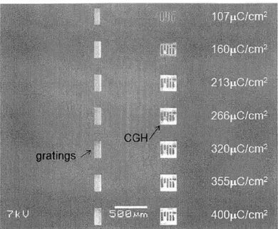
A scanning electron microscope (SEM) image of an example of a dose experiment
for the in-line CGH manufactured on a silicon substrate is shown in Figure 2.1.4. Chirped gratings were written at each dose as well as the CGH mask in order to evaluate the writing characteristics (line edge roughness, minimum resolution, etc.) decoupled from the complex CGH structure. From this experiment, we can see that for the smaller doses, the hologram is underexposed and the HSQ is overly removed
by the developer. Also, several other patterns are overexposed and a substantial
amount of HSQ is left over after development where they should be cleared out due to proximity effects as explained later. The best hologram in this case has a dose of
320pC/cm2 (Figure 2.1.5). Figure 2.1.6 shows a comparison between the over and under dosed cases for the in-line CGH fabricated on a silicon substrate.
Figure 2.1.8 shows an SEM image of the fabricated in-line CGH for the design shown in Figure 2.1.7. Note that the periodicity of the fringes have become more uniform across the structure. This is due to the redistribution of the energy on the
CGH, done through a virtual diffuser [25]. Figure 2.1.9 shows more close-up SEM images of the fabricated CGH. Highly complicated features are reproduced clearly
Figure 2.1.5: SEM image of the fabricated CGH with design shown in Figure 2.1.1
down to smaller than 200nm.
Figure2.1.10 shows a comparison of a section of this hologram with the original
CGH pattern. Most of the patterns on the mask, including many of the finer details,
are transferred with high accuracy onto the HSQ. However, additional optimization steps, such as dose matrices with smaller dose steps, are required in order to get the exact pattern reproduced. In addition, the results from the sensitivity analysis explained in a later section can be used to redesign the CGH mask to compensate for different manufacture errors.
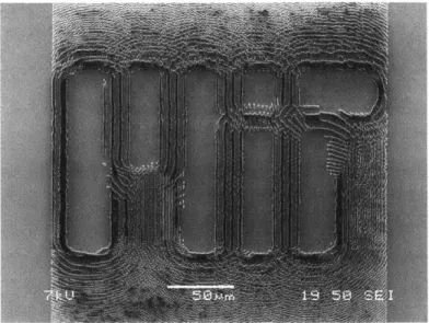
The second fabricated design was that of Figure 2.1.2 that reconstructs a grating matrix at the photoresist plane 50im away. Figure 2.1.11 shows an SEM image of a fabricated CGH for the reflection pattern. This CGH was fabricated with the Raith
150 system at 10keV, and the dose was varied across the structure to compensate for
the proximity effect.
The dose at each section of the pattern was determined through a dose matrix, in which small sections were compared to the original design and the best-fitting dose was determined for each section. Figure 2.1.12 shows a comparison of the fabricated pattern with different doses at two different locations within the mask. It can be seen that different dose are required for different features on the CGH.
(a)
(b)
Figure 2.1.6: Comparison of fabricated CGHs with (a) over- and (b) under-exposure.
Evaluation of Fabrication Accuracy
The fabricated CGH patterns contain geometrical distortion due to fabrication errors such as non-ideal dose of the e-beam, proximity effects, stitching errors, positioning of the beam and the stage in the e-beam writing system, etc. In order to quantitatively evaluate these errors, first, a 2D error map was computed using a spectral based cross-correlation algorithm using data from a confocal microscope. Second, a global mean square error (MSE) was computed and used as a point of comparison between different fabricated samples. Finally, the expected reconstructed intensity at the photoresist from the actual fabricated sample (sample with fabrication errors) is simulated.
Figure 2.1.16 shows the block diagram of the evaluation algorithm. The first step in this algorithm consists of capturing confocal microscope images of the fabricated samples such as those shown in Figure 2.1.14. These images require high magnification and due to the limited field-of-view of the confocal microscope, multiple images from a single CGH must be taken.
The second step consists of noise reduction with a binarization processes. Then the subimages are stitched together with the result shown in Figure 2.1.15 for an example of a fabricated sample. In order to compare the resultant binary image of the fabricated sample with the original design, the image needs to undergo a rotation, scale and lateral shift correction processes. These processes are computed using the
-2.5
2
1.5
-200
-250 -20 -150 -100 -50 0 50 100 150 200
Figure 2.1.7: Design of in-line CGH optimized using the simulated optical diffuser initial guess.
spectral correlation algorithm shown in Figure 2.1.16. An example of a cross-correlation map is shown in Figure 2.1.17. After computing the cross-cross-correlation map, the peak magnitude and position are extracted and are used to estimate the adequate lateral shift, scale and rotation parameters.
The last step consist of the computation of a 2D error map (Figure 2.1.18) and a global error metric based on the MSE of the difference between the fabricated and the designed CGH patterns. The 2D error map is very useful to understand what sections of the fabricated pattern require more or less proximity effect compensation (dose correction). Alternatively, the original pattern could get modified, for example by thinning the fringes, so that after fabrication the sample is compensated for proximity effects.
Spectral correlation is computationally efficient compared to spatial cross-correlation. This method can be automated in order to evaluate the fabricated sample. The error was calculated to be approximately 10%.
As a final evaluation step the expected intensity distribution of the fabricated sample is computed. Figure 2.1.19 shows a comparison of the desired intensity from
Figure 2.1.8: SEM image of the fabricated CGH with design shown in Figure 2.1.7
the original design and the expected intensity from the fabricated CGH of sample 7.
A comparison between the original CGH pattern and sample 7 is shown in Figure
2.1.20. It is clear from this figures that the 10% residual error of this sample reduces the holograms diffraction efficiency allowing undesirable diffraction orders to distort the reconstructed pattern.
2.1.3
Optical Characterization
An optical setup was design to perform the optical characterization of the fabricated
CGH. The optical setup is shown in Figure 2.1.21. A green laser (532nm) is spatially
filtered and collimated to produce a plane wave that probes the fabricated in-line holo-gram with an incidence angle normal to the surface of the holoholo-gram. The diffracted
Figure 2.1.9: SEM image of the fabricated CGH with design shown in Figure 2.1.7
field is imaged by a 100x (NA = 0.75) microscope objective onto a 16 megapixel CCD
with pixels of 9pmx9pm. The microscope objective and CCD are placed on top of a motorized linear stage with an axial resolution of 1pm that allows axial scanning.
Figure 2.1.22 shows the reconstructed intensity distribution from the fabricated hologram of the design of Figure 2.1.7. The reconstructed pattern shows good contrast and well defined edges of the letters which indicates that many of the high spatial frequency fringes survived the fabrication process. Any errors in the fabrication cause lower diffraction efficiency than that of the original design giving rise to more visible background noise.
2.1.4
Exposure Test
In terms of the reflection grating patterns, we have conducted a printing experiment onto a photoresist in order to characterize the actual exposure characteristics of the
CGH. A 364nm laser was used for the exposure in an in-line configuration, for which
the CGH has been designed. Figure 2.1.23 shows the exposure results obtained from this experiment, compared with the predicted intensity distribution at the photoresist for the fabricated sample of Figure 2.1.20. Many of the grating patterns have clearly been reproduced, while some sections are washed out, which resemble the simulated exposure result as expected.
(a)
(b)
Figure 2.1.10: Comparison of fabricated CGHs with design for the same section.
be regarded to be due to experimental errors. First, the exact dose required for the photoresist was unknown, and further experiments and data are needed to obtain the exact dose required to generate the ideal grating pattern. Second, the experimental setup for the exposure was not ideal for the required working distance of 50pm and a depth of focus (DOF) of +0.3pm, and practical difficulty aroused in adjusting the working distance within the DOF. This problem can be alleviated by designing the working distance and the DOF of the CGH to be much larger. Third, the develop-ing conditions for the photoresist also needed further experiments and optimization. Lastly, the drying process after the development can also play a critical role in pro-ducing the gratings.
2.1.5
Conclusion
The feasibility of computer generated holographic technology for high-resolution and high-throughput lithographic applications was investigated. The design flexibility, reconstruction quality, simplicity of system and life span makes CGH technology a promising technology. Experimental fabrication process and systematic evaluation of fabricated samples was performed. A sensitivity analysis to understand the
Figure 2.1.12: Comparison of various dose conditions at various sections of the
pat-tern. Note that while 1.25pC/cm2 (left side) is a better dose for the features in the
top row, the features in the bottom row require a dose of 80pC/cm2 (right side).
tions of potential manufacture errors was implemented.
2.2
Multi-spot Ablation System for LCD Pixel
Re-pair Using a Blazed Grating Matrix
As the demand for larger liquid crystal displays (LCDs) and lower prices grow quickly, the ability to repair any manufacturing defects within the manufacturing process line becomes crucial. Further, being able to do this efficiently is an advantage to the
manufacturer.
In this Section, a system for multi-spot ablation will be introduced. Two main types of defects were considered: open defects (open circuits) and closed defects (left over residue, redundant circuits). For the open defect type, the missing patterns are deposited by means of a laser chemical vapor deposition (LCVD) process. For the
Figure 2.1.13: Block diagram of CGH evaluation algorithm.
Figure 2.1.14: Example confocal microscope data of the reflection grating CGH.
closed defect type, the residual material is eliminated by means of an ablation process. The proposed system will be designed to perform the following three tasks: 1. Metal deposition for the correction of open defects, 2. Laser ablation for the correction of closed defects, 3. Monitoring/imaging for the inspection of the pixel before/after correction.
The system will form high-energy spots in the form of a matrix on the substrate with 30 pam separation between each other. Some of the main challenges of the system include design of the optical system using cost effective methods and meeting the resolution criteria while maintaining the large operation area, as well as fabrication
I0
1100 1200
1 C1. 3O 0 40 0 1110 :3 3 90
Figure 2.1.15: Example of binarized and stitched data: (left) desired CGH; (right) actual fabricated CGH.
hs- HpX xCorr
hf fabitm Imn Hf aIricta s'ak* H acat
Measure: - Peak magnitude - Peak position
Figure 2.1.16: Spectral cross-correlation method.
2.2.1
Design of the Optical System
Figure 2.2.1 shows a schematic of the entire system. In this section, we will go over the functionality and characteristics of each component, as well as choice of parameters or devices.
Objective Lens
The objective lens was chosen to meet the requirements to have high numerical aper-ture, a working distance of over 10mm, and also a small effective focal length. We
xCorrelation Metric
X104
10 200 9 8 400 -7 600 00-1000 3 1200 2 11 200 400 600 800Figure 2.1.17: Example of cross-correlation map.
Table 2.2.1: Specifications of Mitutoyo M Plan Apo NUV 100x [11]
Working Numerical Focal Depth of
Distance Aperture Length Resolution Focus
11.0mm 0.50 2mm 0.6pm 1.1pm
have found the Mitutoyo M Plan Apo NUV 100x lens [11] to be the optimum choice for our application. Specifications of this objective lens are shown in Table 2.2.1.
Relay Optics
Relay optics between the objective lens and the grating matrix is important in order to provide more flexibility in the design of the system, considering the fabrication limitations of the grating matrix. In addition, the diffraction artifacts resulting from the elemental grating cell finite size are minimized. The selection and optimization
~10.
3D -20X -i0 D 1n 2] 3]
Figure 2.1.18: Error Map of the best fabricated reflection grating.
of the optics used is discussed in the next Section.
Grating Matrix
The grating matrix consists of an array of gratings with different pitch and orientation. The purpose of this component is to steer the beam so that the spot at the image plane is precisely at the required location. As was seen in the previous section, the size of the gratings, as well as their design, play an important role in the design of the system. We designed both binary and blazed gratings to obtain high efficiency in the required diffraction order, and the former was fabricated with conventional optical
Figure 2.1.19: The designed reconstructed intensity (left) and the numerically recon-structed intensity of the fabricated CGH.
lithography, and the latter was designed to be fabricated with gray scale lithography. Details of the design and fabrication methods will be discussed in a later section.
Spatial Light Modulator (SLM)
A spatial light modulator (SLM) is used in our system to control the on/off of each
ablation spot, as well as to compensate for the variation in efficiency of the multiple gratings with different pitches. In general, there are two types of SLMs, micro-actuated mirrors such as Boston Micromachines deformable mirrors [6] and Texas Instruments digital micromirror devices (DMDs) [7], and liquid crystal (LC)-based modulators such as ferroelectric liquid crystals (FLCs) and twisted nematic liquid crystals (TNLCs).
In the case of the discussed system, the LC modulators are more suitable for the following reason. In this system, all beams must have equal power at the exposed substrate in order to have proper ablation characteristics. However, due to variation in diffraction efficiencies from the gratings, the intensity of each beam must be tuned individually. This tuning can be done by an LC light modulator, since the device has capabilities of tuning the attenuation of the beam passing through. Note that even though digital mirrors can also attenuate light, this is through high-frequency vibration of the mirrors, which is not applicable to pico-second pulsed lasers.
In our setup, we installed the LCoS system from Holoeye [9] due to its availability as an integrated device. Figure 2.2.2 shows the installation of the device in the setup.