HAL Id: hal-01387072
https://hal.archives-ouvertes.fr/hal-01387072
Submitted on 28 Oct 2016
HAL is a multi-disciplinary open access
archive for the deposit and dissemination of
sci-entific research documents, whether they are
pub-lished or not. The documents may come from
teaching and research institutions in France or
abroad, or from public or private research centers.
L’archive ouverte pluridisciplinaire HAL, est
destinée au dépôt et à la diffusion de documents
scientifiques de niveau recherche, publiés ou non,
émanant des établissements d’enseignement et de
recherche français ou étrangers, des laboratoires
publics ou privés.
simulation: Extraction of turn-on elements
Fabien Escudié, Fabrice Caignet, Nicolas Nolhier, Marise Bafleur
To cite this version:
Fabien Escudié, Fabrice Caignet, Nicolas Nolhier, Marise Bafleur. From quasi-static to transient
system level ESD simulation: Extraction of turn-on elements. Electrical Overstress/Electrostatic
Discharge Symposium (EOS/ESD), 2016 38th, ESD Association, Sep 2016, Anaheim, United States.
pp.1 - 10, �10.1109/EOSESD.2016.7592563�. �hal-01387072�
From Quasi-static to Transient System Level ESD
Simulation: Extraction of Turn-on Elements
Fabien Escudié (1), Fabrice Caignet (1), Nicolas Nolhier (1), Marise Bafleur(1)
(1) LAAS-CNRS, Université de Toulouse, CNRS, UPS, Toulouse, France tel.:05 61 33 62 00, e-mail: [email protected].
Abstract – Transient simulation is a main challenge to achieve system level ESD failure prediction. During the turn-on of
the protections, complex phenomena introduce complex transient behaviors. In this paper we investigate the parameters that have to be added to perform accurate transient simulations and we propose a methodology to extract them by measurements.
I. Introduction
Achieving efficient system level electrostatic discharge (ESD) reliability is a main challenge in embedded systems. As there are more and more embedded systems, they are exposed to severe environments and the failure requirements are growing in importance. The analysis and understanding of malfunction is usually very difficult. The ESDA (ESD Association) industry council has pointed out the importance in performing System Efficient, ESD Design (SEED)[1]. Several studies were done in order to predict the impact on systems of electrical fast transients using a behavioral simulation [2,3,4,5,6]. The models created by I(V) curves obtained from Transmission Line Pulse (TLP) allow quasi-static simulations. In these papers good measurement correlations are obtained when the rest of the system is modeled with a high level of accuracy. However, an accurate transient behavior cannot be obtained with this simple I(V) model. The dynamic turn-on behavior of the protection can have a large influence on the overshoot or on the time to trigger and up to now this has not been studied except one that will be discussed [14]. A method to predictive ESD simulation is being developed in seven labs within the ESD association working group WG26: “Models for system level simulation”. The main goal is to cover a wide range of ESD protections like the ones in digital, fast communication and automotive components. This work focuses on a LIN (Local Interconnect Network) for automotive applications. Three different products are tested, that allow testing three different on-chip protections. Thanks to these differences we will investigate different transient behaviors.
The developed board to inject the ESD stress and measure the corresponding response will be presented in the first chapter. The measurement setup will be described in detail with its frequency limits. The next paragraph will summarize how conventional modeling approach is performed, and the models built for the three devices. In
this section the model of the devices is built from quasi-static I(V) TLP measurements.
One of the first important goals of modeling is the validation of the models. In the following section two case of configuration are presented: without external elements and with an external decoupling capacitance. We have chosen an external decoupling capacitance because when a snapback protection turns on, the discharge of the capacitance into the device is mainly limited by the on-chip transient parameters. In our opinion, it represents one of the most complex transient event, exhibiting a very high current discharge into the chip, which is only limited by the transient behavior of the protections. For each configuration the three devices are tested and the validity of the “basic” model is discussed.
The observations will confirm that transient parameters are needed to accurately reproduce voltages and current waveforms. In this paper we proposed to obtain transient parameters from TLP measurements. Two main parameters are extracted: the first one just before the turn-on of the protection, to be sure that the transient charge of the input pin device is reproduced and a second one, reproducing the dynamic turn-on behavior of the protection. The extracted parameters allow generating an advanced model, and we will demonstrate the benefits of the model on the cases of study. A description to build the model and the experienced difficulties are detailed. Finally, two LIN boards are connected with a cable and the injection is made between them. The objective is to predict how the on-chip protections behave.
II. System under test
The main goal of this study is to validate the classical SEED modeling approach that is presented in most of the papers. Following this objective, a dedicated PCB has been developed in order to allow various injections, have multiple system configurations and to be able to perform voltage and current measurements. The system under test is
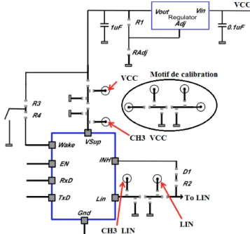
based on a LIN (Local Interconnect Network) driver, and three different suppliers with the same pins assignment are tested, allowing comparing three different protection’s strategies. The schematic diagram of the board is reported in figure 1.
Regulator
Figure 1 : Schematic of the LIN board.
The LIN driver is an eight-pins device with one power supply (Vsup), one ground (gnd), the output communication wire (LIN) two control mode signals (Wake & INH) and 3 pins connected to a microcontroller (EN, RxD & TxD). Among these pins, only two are connected to the outside world and are supposed to undergo ESD events. So the IC models will be built between Vsup, GND and LIN pins. As reported in figure 1, the system can be powered using a LM312 regulator with its decoupling capacitances. A picture of the board is given in figure 2.
Figure 2 : Schematic of the LIN board.
Figure 3 : Injection pattern used on board.
The same injection pattern (fig. 3) is printed on the board in order to test pins that can be exposed to stress (LIN & Vsup). All the PCB lines have a 50Ω-impedance. The patterns allow both measurement and injection techniques. The discharge from SMA_injection can be modulated with external elements placed on footprints 1 to 5. On the right part of the board (fig. 2) a dedicated calibration pattern is placed to calibrate each configuration used into the tests. The SMA connectors Vsup and LIN allow the injection (SMA_Injection – fig 3). CH3_VSUP and CH3_LIN allow the voltage measurement by adding a 500 Ω resistance on footprint 6. Using such resistance value, in parallel to the 50 Ω lines, we get an attenuation of 21dB. This on-board dedicated probe has been characterized in the frequency domain using Vector Network Analyzer (VNA) and exhibit a good linearity up to 1GHz. (Fig. 4).
Current measurement is carried out using a near field probe placed above a micro strip line [8,9,10]. The induced voltage from the magnetic field is computed in the frequency domain to reconstruct the current through the stripe line. The frequency response on the probe has been precisely measured using the calibration pattern and a VNA (Fig. 5). We can observe that the S21 parameter has a +20dB/Dec slope that confirms the purely inductive coupling effect between the probe and the PCB line. As for the voltage probe, the near field probe allows having 1GHz bandwidth. Both probes have been calibrated taking into account the resistances inserted in the path of the ESD stress to be sure that it will not induce artifacts.
!40$ !35$ !30$ !25$ !20$ !15$ 10$ 100$ 1000$ Ga in $(d B) $ Frequency$(MHz)$
Figure 4 : Frequency response of the PCB voltage probe.
!75 !70 !65 !60 !55 !50 !45 !40 !35 !3010000000 100000000 1E+09 1E+10 S21.Current.probe
III. Conventional model
generation and system simulation
Following the methodology presented in most papers dealing with SEED, behavioral models are created with quasi-static measurements performed using a TLP tester. Usually the TLP have a 100 ns and a rise time around 1 ns. The exposed pins are measured (between ground and power supply), and a behavioral on-chip strategy is built. The compact models of the protection are made up using a piecewise linear description.
In the paper, we will follow the same method to build the model and we will show that it could induce strong error depending on the system configuration. The component’s pins are tested in pairs with positive and negative pulses. For the Lin device only one pin is exposed to the outside world, and three pins are measured (LIN, GND, VDD pins). Figure 6 reports the LIN to GND I(V) curves obtained from three different providers called (A,B,C).
0 2 4 6 8 10 12 14 16 18 0 10 20 30 40 50 60 70 80 A C B
Figure 6 : I(V) curves of the 3 LIN components for positive pulse on LIN-GND pins.
Piecewise linear models are developed from the TLP measurement data (fig.7). The Ix,Vx points describe the ESD protection by piecewise segment, which is included in simulations like state machines in VHDL-AMS [11]. For the component C, the model of fig. 7 (a) is used. For components A and B that exhibit a strong snapback, the model of figure 7(b) is used with a strong non-linearity. Such model describe in VHDL-AMS can be found in Erreur ! Nous n’avons pas trouvé la source du renvoi..
(a) (b)
Figure 7 : IV curves « linear » and « non-linear » piecewise modeling.
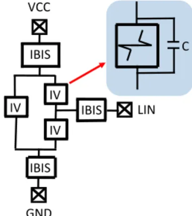
The LIN component is composed by the I(V) curves obtained between the LIN, VSUP and GND pins with the IBIS information (R package, L package and C package) [12] associated. The three devices have exactly the same electrical schematic, only the description of the protections is different. As they have the same package, the parasitic elements (Rpck, Lpck and Cpck) are the same (even if some small differences can exist.)
IV# IBIS# IBIS# IBIS# C# VCC# LIN# GND# IV# IV#
Figure 8 : Schematic diagram of the Lin component .
The whole measurement setup, the transmission lines and the PCB are reproduced in simulation (fig. 9). The TLP generator is made of a transmission line, the 1ns time rise filter is made of RLC elements [13], the attenuator is represented by a T of resistors, all cables are inserted as a transmission line and the PCB is introduced in simulation as LC distributed elements.
HV#
1MΩ# TLP##Line# Filtre#1ns## A3# Line#i#TLP# Line#
v#TLP# PCB# Model## Capa# HF# 500Ω# 50Ω# V#DUT#LIN# VCC# LIN# GND# 500Ω# 50Ω# V#DUT#VCC#
Figure 9 : Schematic diagram of the whole simulated system.
IV. Simulation analysis
In a first step, only TLP injection is done. This allows a better understanding of the phenomenon we want to characterize. Each time, simulation is compared with voltage and current measurements, but depending on the analysis, only the most significant observations will be reported. First, the quasi-static simulation results are investigated to establish the validity of using piecewise linear model and its limits. Next transient simulation is investigated to clearly show the inaccuracies in the methodology.
A. Quasi-static simulation
Figure 10 & 11 report the voltage measurement and simulation for 100V, 400V and 800V TLP injection respectively. If we look at the plateau of the waveform, the
simulated voltage fits perfectly with the measurements as expected. We can just notice that the measurement of 100V TLP injection on the B component shows a continuous increase of the voltage until the protection triggers at around 30ns. The model extracted from the TLP measurements could not be reproduced, because the I-V points are computed at around 80ns.
!20$ 0$ 20$ 40$ 60$ 80$ 100$ 120$ 140$ 160$ 0,00$ 20,00$ 40,00$ 60,00$ 80,00$ 100,00$ Measure$100V$ Measure$400V$ Measure$800V$ Simula5on$100V$ Simula5on$400V$ Simula5on$800V$
Figure 10: Comparison of voltage measurement with simulation with no external elements for component A – TLP injection 100V,
400V, 800V. !40$ !20$ 0$ 20$ 40$ 60$ 80$ 100$ 120$ 0$ 20$ 40$ 60$ 80$ 100$ Measure$100$ Mesure$400$ Mesure$800$ Simula3on$100$ Simula3on$400$ Simula3on$800$
Figure 11: Comparison of voltage measurement with simulation with no external elements for component B – TLP injection 100V,
400V, 800V.
B. Transient simulation
Such result is predictable but we are also interested by the response of the model with an external component like a decoupling capacitance of 1nF on the LIN input. The main point is to validate the model whatever the external component is placed around the device. Even if it looks as a simple device, an external decoupling capacitance introduces complex phenomena. Figure 12 reports measurement and simulation with and without a 1nF capacitance placed in parallel to the input of the LIN for component A (The configuration without this capacitance is
also reported), 100V TLP injection. In this simulation the output capacitance is modeled with its high frequency parameters extracted using VNA.
!10$ 0$ 10$ 20$ 30$ 40$ 50$ 60$ 70$ 80$ 0$ 10$ 20$ 30$ 40$ 50$ 60$ 70$ 80$ 90$ 100$ 110$ 120$ Measure$with$C$ Simula;on$with$C$ Measure$without$C$ Simula;on$without$C$ Vo lta ge ((V ) Times((ns)
A
B
C
A
B
C
Cu rre nt (A ) Times.(ns) !2,0% 0,0% 2,0% 4,0% 6,0% 8,0% 10,0% 12,0% 14,0% 16,0% 0% 10% 20% 30% 40% 50% 60% 70% 80% 90% 100% 110% 120% Simula4on%with%C% Measure%with%C% Measure%without%C% Simula4on%without%C%Figure 12 : Comparison between simulation and measurement for voltage and current on LIN-GND pin (component A), 100V TLP
injection.
These curves can be divided into 3 parts, the charge of ESD protection before the triggering voltage (A), the time from peak voltage to give a stable level (B) and the quasi-static level (C). The simulations matched well during the first and the third state. In area B, the current through the component is much more important in simulation caused by a fast discharge of the capacitance (strong snapback). It appears that another phenomenon controls the current path just after the triggering of the protection. The on-resistance extracted from TLP I(V) measurement is not the one foreseen by the protection during a few nanoseconds. This can be observed on the voltage (measure and simulation) without the capacitance. On measurement, after the triggering of the protection, the voltage continues to increase (5V) and the first peak is larger than the simulation one. At 30V the voltage decreases slowly to its stable value at t=25ns. Figure 13 reports the transient measurements obtained, with a 100V TLP injection between LIN and GND pins for component B. Quasi-static simulations exhibit a perfect correlation with the measurements for voltage and current levels at 80ns. But the measurements show that from 0 to around 30ns the voltage increased slowly. Following the classical model methodology, the simulation is not able to predict this (fig.13 – Simulation 1). To take into account such transient events into the simulation, additional parameters must be added. The next paragraph details what
parameters we chose and the way to extract them from measurements. !5# 5# 15# 25# 35# 45# 55# 65# 0# 20# 40# 60# 80# 100# 120# Measure# Simula5on#2# Simula5on#1# Vo lta ge ((V ) Times((ns) !0,2% 0% 0,2% 0,4% 0,6% 0,8% 1% 1,2% 1,4% 1,6% 1,8% 0% 20% 40% 60% 80% 100% 120% Measure% Simula4on%1% Simula4on%2% Cu rre nt (A ) Times.(ns)
Figure 13: Comparison between simulation and measurement for voltage and current between LIN and GND pins with 100V TLP
injection (component B).
IV. Model extension with transient
parameters
A. Charge parameter extraction
The input capacitance of the device often added into the simulation reflects the time to reach the triggering voltage. This parameter could be obtained from the data sheet or is given into IBIS models. Most of the time, it is obtained using a VNA, which means a small signal analysis. This part is mostly purely passive. Looking at the measurement in figure 13, it is clear that during high injection, the behavior of the element(s) before the triggering of the protection could be non-linear. In this case, we make the assumption that it looks like a “non-linear capacitance” (even if it could be physically related to some active parts). The next step is to find a way to extract this “non-linear capacitance”. We built a set-up using a high precision capacitance (COG type) placed in parallel in footprint 3 (fig. 3) to get I(V) curves before the triggering voltage level. We calibrate this 1nF capacitance to be sure that it has a stable value from 0V to the triggered voltage level (around 70V). This capacitance will slow down the charge. Figure 14 reports the I(V) curves obtained at 80ns for the 1nF capacitance and the three components.
Component A follows the measurement of the 1nF capacitance. This confirms that before the snapback the behavior is purely capacitive. Component B shows a change (around 30V) that reflects an on-chip active part, then, it seems to increase as a capacitance up to 50V
0 0,1 0,2 0,3 0,4 0,5 0 10 20 30 40 50 60 Reference/1nF Component/A Component/B Component/C Voltage((V) Cu rr en t(A )
Figure 14: I(V) curves before triggering voltage with 1nF capacitance between LIN and GND pins.
!0,1 !0,05 0 0,05 0,1 0,15 0,2 0,25 0,3 0,35 0,4 0 20 40 60 Ca pa ci ta nc e2 (n F) Voltage2(V) A B C
Figure 15: Equivalent capacitance of the LIN_GND protection.
In figure 15, the capacitance value from figure 14 is extracted using the charge capacitance formula (1 & 2).
€ uc(t) = E × (1 − e−τt) + Vini × e−τt (1) € c = − t R × ln(uc(t) − E Vini − E) (2)
Where Uc(t) is the dynamic voltage, Vini is the precharge voltage of the capacitance, E is the TLP charge voltage and
τ
the time constant of the RC network. To get figure 15, the time corresponds to the one chosen for the voltage measurement on the TLP waveform (t=80ns), and the initial voltage is Vini=0. The capacitance C is calculated assuming that the resistance is 50 Ω.One of the most important results is that we succeed to get the input capacitance during the stress of component A (50pF). For component B we get a 30pF from 0V to 30V then something looking like a 300pF upon the turn on of the protection. For component C we obtained 70pF. If we look at the transient voltage curve v(t) with 80V TLP injection (fig.16), there is a change in capacitance charge at 24V. !5# 5# 15# 25# 35# 45# 55# 65# 0# 20# 40# 60# 80# 100# Cref#=#1nF# Cref+Dut#B# A B Reflection area Vini2 1 B Times2(ns) Vo lta ge 2(V ) τ !2
Figure 16: LIN-GND v(t) curve at 70VTLP for the component B with 1nF external Capacitance in parallel.
The capacitance corresponding with τ1 calculated in the A area is 30pF. In the B area the first 300pF obtained were calculated assuming that the initial voltage was zero and so the 300pF is not correct. We need to readjust Vini and the time in equation (2). Taking into account the appropriate values, we found a 600pF capacitance for the LIN-GND protection on the B area. A variable capacitance for which the value is related to the voltage was introduced in the model and the simulation result is shown in fig.13 (Simulation 2).
B: Dynamic turn-on parameter
extraction
If we focus on the two components A and B, they both have different turn-on conditions. Looking at the transient behavior, without external decoupling capacitances, the component B exhibits a quick turn-on, as the component A seems to have two different slopes when the voltage reaches its stable snapback value. When simulations are performed without external capacitances, this is not really important and both simulations give accurate results for both voltage and current. With the capacitance, a strong error is observed on the current simulation. This is mainly due to the prediction of the speed of the discharge into the component. Using a protection model based only on TLP measurements introduces a quasi-static resistance of around 1Ω that generates in the simulation a current discharge of 16A, and the measurement does not exceed 6A. An additional turn-on parameter is needed.
Recently, in paper [14], a first interesting transient modeling has been proposed. The model focuses on the transient aspect of the turn-on. No real parameter is extracted and a behavioral model is built using an equivalent dynamic resistance and an equivalent voltage
generator. This equivalent Thevenin model is built step by step in time domain. For each time point, the equivalent generators and resistances are extracted from the transient voltage response of the protection under TLP stress. This give a R(t) and E(t) parameters.
In this paper we propose to build an equivalent SPICE schematic of the protection that represents both its static and dynamic responses. The main idea is that during transient the velocity of the operating point is driven by a higher resistance than the one get by TLP. We assume that the model built around quasi-static measurement can be enhanced with a dynamic part (Zdyn) as reported in figure 17.
The generator Ep and the Rstat resistance represent the quasi-static equivalent model of the protection when the device turns-on. These two parameters are extracted from the quasi-static I(V) curve. Cp represents the equivalent capacitance to define the charge slope (just before the triggering). This capacitance also impacts the turn-on speed. This parameter has been extracted in the previous paragraph.
To represent the dynamic aspect, a set of resistance Rdyn, in parallel with an inductance Ldyn is used. When the protection triggers (t0+ε), the dynamic inductance passes no current and all the current goes through Rdyn. Instantaneously the equivalent serial resistance of the protection is Rdyn+Rstat. After few nanoseconds, depending on the value of Ldyn, the inductance acts as a short circuit reducing the serial resistance to Rstat. Rdyn and Ldyn form the dynamic impedance Zdyn.
Rstat
Ldyn Rdyn
Cp
Ep
Zdyn
Figure 17: Equivalent electrical schematic of the protection when it turns-on.
On this paper we propose to directly extract Rdyn from TLP measurements and to adjust Ldyn by looking at the transient responses. The theory applied to extract the dynamic resistance is the same as the one used to get the dynamic resistance as applied to the small-signal behaviour of a semiconductor like diode or MOS devices [15]. Basically, to calculate the operating point of the snapback device under TLP stress, we plot the static load line (or DC load line) over the electrical mounting. During the triggering of the protection, we consider that a dynamic resistance drives the voltage and current. And so, the transient response follows the dynamic impedance represented in the dynamic load line (or AC load line).
From the transient response of the device to TLP, an I(V) curve is traced and reported in Fig. 18 for the component A and Fig 19 for component B. The quasi-static response of the protection is reported in red. The green, purple and blue curves are the dynamic responses of the protections for 100V, 400V and 800V TLP injection respectively. In the two figures, we draw the dynamic load line that fits the most linear part of the curves (400V & 800V). For component A, these two lines are perfectly parallel, meaning that the dynamic resistance must be the same whatever the value of the voltage across the protection. The extraction of the dynamic resistance for component A resulted in Rdyn = 8Ω. In figure 19, the two load lines are not perfectly parallel. As the protection is faster than the previous one, the linearity is less defined, the inductance effect is more important. Nevertheless, on the linear part, we get Rdyn = 11Ω for 800V and 18Ω for 400V. In this case, the dynamic resistance could be a function of the current. In the simulation reported in this paper, we will fix it at 15Ω. For the component C, the same methodology is used to get Rdyn= 11Ω (not reported here).
!2,00% 0,00% 2,00% 4,00% 6,00% 8,00% 10,00% 12,00% 14,00% 16,00% !40% !20% 0% 20% 40% 60% 80% 100% 120% 140% 160% Cu rr en t%( A) % Voltage%(V)% Measure%100V% Measure%400V% Measure%800V% IV%Model% Dynamic load line 800V Dynamic load line 400V
Figure 18: transient I(V) curves obtained during TLP stress (no external elements) of component A .
!1# 1# 3# 5# 7# 9# 11# 13# 15# !40# !20# 0# 20# 40# 60# 80# 100# 120# Cu rr en t#( A) # Voltage#(V)# Measure#100V# Measure#400V# Measure#800V# IV#model# Dynamic load line 800V Dynamic load line 400V
Figure 19: transient I(V) curves obtained during TLP stress (no external elements) of component B.
V. Validation of the extended
transient models
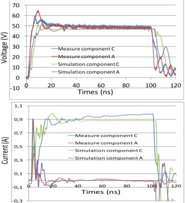
After extracting from TLP measurements additional charge parameters and dynamic turn-on parameters, a new model is built for each A, B, C components. The results shown take into account the decoupling capacitance of 1nF placed in parallel, which exhibits the most complex discharge events.
Figure 20 reports the comparison between measurements and simulations of the basic model and the extended one taking into account the transient parameters. 800V and 100V TLP injection are compared. Looking at 800V injection, the advanced model is perfectly able to reproduce both the voltage and the current waveforms (overshoot and pulse duration). The current reaches 24A for a 14A injection. This means that the model is perfectly able to reproduce the transient turn-on of the snapback protection. For 100V injection, there are small differences on the voltage. Regarding the current, the peak amplitude is reduced from 16A to 10A, and the measured value is 6A. For such small injection level, our model seems to be not accurate enough. If we look at the figure 12, the component A exhibits a turn-on in two parts: a first one very quick, and a long voltage decrease from 5 to 20ns. This second turn-on phenomenon (somehow not classical) is not reproduced by our modeling method.
!10$ 10$ 30$ 50$ 70$ 90$ 110$ 0$ 10$ 20$ 30$ 40$ 50$ 60$ 70$ 80$ 90$ 100$ 110$ 120$ Measure$800V$ Basic$model$800V$ Advanced$model$800V$ Mesure$100V$ Basic$Model$100V$ Advanced$model$100V$ !10$ !5$ 0$ 5$ 10$ 15$ 20$ 25$ 30$ 0$ 10$ 20$ 30$ 40$ 50$ 60$ 70$ 80$ 90$ 100$ 110$ 120$ Measure$800V$ Basic$Model$800V$ Advanced$model$800V$ Mesure$100V$ Basic$model$100V$ Advanced$model$100V$
Figure 20: Comparison between simulation and measurement for voltage and current between LIN and GND pins with decoupling
In figure 21 the measurements of component C are compared with the models. The triggering voltage of this protection diode is around 40V. In general, the advanced models give better accuracy than basic I(V) ones. The overshoot (70V for 400V injection & 95V for 800V injection) is well reproduced.
If we look into details, on the voltages, for 400V injection, with the advanced models, the simulated waveform is below the measured one, which is the opposite for 800V injection. The overshoot is meanly related to the inductance effect. This means that the Ldyn we put into the model is higher than the equivalent one found in the device. We define Ldyn for each component by fitting the turn-on speed. A good way to extract this parameter has to be found for better accuracy. Another point is that for 400V TLP injection Rdyn extracted using the method proposed in chapter IV.B is 11Ω and 6Ω for 800V. In the simulation we implemented Rdyn of 10Ω. If the resistance increases, the overshoot is increased. It means that the model of the dynamic resistance has to be carefully tuned.
0" 20" 40" 60" 80" 100" 0" 10" 20" 30" 40" 50" 60" 70" 80" Vo lta ge(( V) ( Time((ns)( Measure"800v" Basic"Model"800V" advanced"model" 800V" Measure"400v" Basic"model"400V" Advanced"model" 400V" 0" 2" 4" 6" 8" 10" 12" 14" 16" 18" 20" 0" 10" 20" 30" 40" 50" 60" 70" 80" Cu rr en t'( A) ' Time'(ns)' measure"800V" Basic"Model"800V" advanced"model"800V" Measure"400V" Basic"Model"400V" Advanced"model"400V"
Figure 21: Comparison between simulation and measurement for voltage and current between LIN and GND pins with decoupling
capacitance (component C).
Looking at the result, adding a dynamic impedance into the model of the on-chip protections significantly increases the accuracy of the simulations. This is even more important if current is investigated. We demonstrated that for high level of injection the proposed model gives very good result on the three investigated components.
VI. Validation with two boards
connected by wires
In this part, we tested two boards based on LIN components connected together with cables, one embedding component A and the other component C.
Figure 22: Schematic of equipment under test
Using such configuration, we wanted to validate our transient model. TLP stress is injected at 10cm from one board including component C and at 20cm to the other with component A. The two components are mounted on board alone, with no external elements. The simulation results are compared to the measurements for multiple values of injected voltage (100V, 200V, 800V). !10 0 10 20 30 40 50 60 70 0 20 40 60 80 100 120 Measure1component1C Measure1component1A Simulation1component1C Simulation1component1A
Vo
lta
ge
((V
)
Times((ns) !0,3 !0,1 0,1 0,3 0,5 0,7 0,9 1,1 0 20 40 60 80 100 120 Measure3component3C Measure3component3A Simulation3component3C Simulation3component3A Times&(ns)Cu
rre
nt
(A)
Figure 23: Measure and simulation results for the LIN-GND protection of C and A components, 100V TLP injection
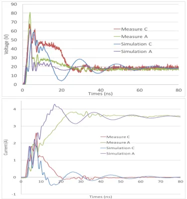
0 10 20 30 40 50 60 70 80 90 0 20 40 60 80 Vo lta ge 2(V ) Times2(ns) Measure2C Measure2A Simulation2 C Simulation2 A !1 0 1 2 3 4 0 10 20 30 40 50 60 70 80 Cu rre nt1 (A) Times1(ns) Measure1C Measure1A Simulation1C Simulation1A
Figure 24: Measure and simulation results for the LIN-GND protection of C and A components, 200V TLP injection.
In figure 23, 100V TLP is injected. Simulation and measurement correlate and all the current goes into the component C. In figure 24, 200V is injected. The behavior is totally different and at this time the component A conducts the current. It takes approximatively 20ns for the system to stabilize, and the simulation gave us around 10ns. We can notice that the measured voltage on component C stays more than 10ns around 40-45V, which is its triggering voltage. 0 20 40 60 80 100 120 140 0 20 40 60 80 100 Vo lta ge .(V ) Times.(ns) Measure.C Measure.A Simulation.C Simulation.A !2 0 2 4 6 8 10 12 14 16 0 20 40 60 80 100 Cu rr en t. (A ) Times.(ns) Measure.C Measure.A Simulation.C Simulation.A
Figure 25: Measure and simulation results for the LIN-GND protection of C and A components, 800V TLP injection.
Figure 25 is obtained for 800V TLP injection. The surprising thing is that even if we have a strong injection, it takes approximately 50-60ns for the system to stabilize. If we look at the current, our simulation is able to predict this long time to distribute the discharge on the two components. The slopes of the measurement and simulation are well reproduced but the started amplitude levels do not match. At this point of study, it is difficult to say if it is due to the triggering conditions of the devices or to a line-modeling problem that drives the stress to on component more quickly then expected.
Conclusion
In this paper we investigated the way to perform transient simulations to predict the impact of system level ESD stress. A dedicated board has been designed around three devices to be sure that the proposed method is applicable for various on-chip protections. Initially, we extracted quasi-static I(V) curves from TLP measurement as done in most of papers addressing SEED. Then the model built from this measurement was compared with simulation. With no external elements, this methodology gives very good results, and the quasi-static voltages and currents can be accurately predicted. When an external decoupling capacitance is added, a lot of mismatches appear showing that transient simulation is required if we want to have accurate prediction. In the measurement and simulation reported, more than 150% of error is observed. To take into account this dynamic behavior into simulation, additional elements that translate dynamic turn-on behavior of the device must be added.
From these observations, we proposed a set of measurement methodologies to extract first an on-chip equivalent capacitance that reproduces the way the voltage increases. Second, we added to the quasi-static model a dynamic impedance made up of a resistance and an inductance in parallel. The dynamic resistance is extracted from a time representation of the I(V) curve, and the inductance is set to fit the time to reach the stable value. This combination of the Rdyn and Ldyn enables the modeling of the relaxing time of the ESD protections.
The enhanced model is compared with measurement in different configurations with different devices and shows a very good accuracy. We demonstrated that it is possible to get transient parameters from TLP measurements that provide transient system level ESD simulations. This work is under progress and it has to be fully validated with ESD gun stresses.
Acknowledgements
The authors would like to thank the French national agency of research (ANR) for its financial support of EFT-SAFE3A project. The authors would also address their thanks to the ESDA, WG26 (models for system level simulation) working group for their support on the boards and discussions on this topic.
References
[1] Industry Council on ESD Target Levels, White Paper "System Level ESD, Part I: Common Misconceptions and Recommended Basic Approaches
[2] N. Monnereau, F. Caignet, D. Trémouilles, "Building-up of system level ESD modeling: Impact of a decoupling capacitance on ESD propagation," Electrical Overstress/ Electrostatic Discharge Symposium (EOS/ESD), 2010 32nd, pp.1-10, 3-8 Oct. 2010 [3] N. Monnereau, F. Caignet, N, Nolhier, D. Trémouilles, M. Bafleur, "
Behavioral-Modeling Methodology to Predict Electrostatic-Discharge Susceptibility Failures at System Level: An IBIS improvement," EMC Europe 2011 York, pp.457,463, 26-30 Sept. 2011.
[4] N. Monnereau, F. Caignet, N. Nolhier, et al. « Investigation of Modeling System ESD Failure and Probability Using IBIS ESD Models », IEEE Trans. on Device and Materials Reliability, Volume: 12 Issue: 4 Pages: 599-606, Dec. 2012.
[5] Tianqi Li; et al., “An application of utilizing the system-efficient-ESD-design (SEED) concept to analyze an LED protection circuit of a cell phone,” Electromagnetic Compatibility (EMC), 2012 IEEE International Symposium.
[6] R. Mertens, E. Rosenbaum, H. Kunz, A. Salman, and G. Boselli, “A flexible simulation model for system level esd stresses with applications to ESD design and troubleshooting,” 34rd Electrical Overstress/Electrostatic Discharge Symposium (EOS/ESD), 2012. [7] Collin Reiman, Nicholas Thomson, Yang Xiu, Robert Mertens and
Elyse Rosenbaum, « Practical Methodology for the Extraction of SEED Models », Electrical Overstress/ Electrostatic Discharge Symposium (EOS/ESD), 2015.
[8] IEC 61967-3: “Integrated Circuits, Measurement of Electromagnetic Emissions, 150 kHz to 1 GHz – Part 3: Measurement of Radiated Emissions – Surface Scan Method”.
[9] F. Caignet, N. Monnereau, N. Nolhier, « Non-invasive system level ESD current measurement using magnetic field probe », International Electrostatic Discharge Workshop 2010, Tutzing (Allemagne), 10-13 May 2010
[10] Wei Huang et al., “Probe characterization and data process for the current reconstitution by near field scan method,” IEEE International Symposium of Electromagnetic Compatibility, June 2010.
[11] IEEE 1076.1, “VHDL analog and mixed-signal,” 1999.
[12] ANSI/EIA-656B, “IBIS (Input Output Buffer Information Specification), www.eigroup.org/IBIS.
[13] Y. Cao, et al. "Rise-Time Filter Design for Transmission-Line Pulse Measurement Systems," in Microwave Conference, 2009 German, pp.1-5, 16-18 March 2009.
[14] Kuo-Husuan Meng, E.Rosenbaum, et al. " Piecewise-Linear With Transient Relaxation for Circuit-Level ESD Simulation ", IEEE Trans. On Device and Materials Reliability, Volume: 15, 3 Sept. 2015.
[15] A.P. Godse, U.A. Bakshi. " Semiconductor Devices & Circuits ", Techinal publication Pune. Chapter 5.2.2, pp.256,259, Edition 2008.