HAL Id: hal-01693979
https://hal.archives-ouvertes.fr/hal-01693979
Submitted on 7 May 2018
HAL is a multi-disciplinary open access
archive for the deposit and dissemination of
sci-entific research documents, whether they are
pub-lished or not. The documents may come from
teaching and research institutions in France or
abroad, or from public or private research centers.
L’archive ouverte pluridisciplinaire HAL, est
destinée au dépôt et à la diffusion de documents
scientifiques de niveau recherche, publiés ou non,
émanant des établissements d’enseignement et de
recherche français ou étrangers, des laboratoires
publics ou privés.
Single-event-transient effects in Junctionless
Double-Gate MOSFETs with Dual-Material Gate
investigated by 3D simulation
Daniela Munteanu, Jean-Luc Autran, S. Moindjie
To cite this version:
Daniela Munteanu, Jean-Luc Autran, S. Moindjie.
Single-event-transient effects in Junctionless
Double-Gate MOSFETs with Dual-Material Gate investigated by 3D simulation. Microelectronics
Reliability, Elsevier, 2017, 76 (SI), pp.719-724. �10.1016/j.microrel.2017.07.040�. �hal-01693979�
Single-Event-Transient Effects in Junctionless Double-Gate
MOSFETs with Dual-Material Gate Investigated by 3D Simulation
D. Munteanu
a, J.L. Autran
a,*, S. Moindjie
aa Aix-Marseille University & CNRS, IM2NP (UMR 7334), Faculté des Sciences – Service 142, Avenue Escadrille Normandie Niémen, F-13397 Marseille Cedex 20, France
Abstract
The Junctionless Double-Gate MOSFET combined with a Dual-Material Gate (JL-DMDG) is interesting for future ultra-scaled devices thanks to a simplified technological process (no junctions), reduced leakage currents and capability to reduce short-channel effects and hot-carrier effects (due to the step in the potential profile induced by the dual-material gate). In this work, we investigate the bipolar amplification and charge collection in JL-DMDG submitted to heavy-ion irradiation. The impact on single-event transients of several parameters such as the length of the high-workfunction gate-material region and of the workfunction of the low-workfunction gate-gate-material region is also particularly addressed. We show that JL-DMDG is more sensitive to radiation than more conventional devices with single-material-gate or operating in inversion-mode.
Keywords
Junctionless Double-Gate MOSFET, Dual-Material Gate, bipolar amplification, single-event transients
* Corresponding author:
Prof. Jean-Luc Autran IM2NP - UMR CNRS 7334 Faculté des Sciences – Service 142 Avenue Escadrille Normandie – F-13397 Marseille Cedex 20 France
Phone: + 33 (0)413 594 627 Fax: +33 (0)491 288 531
Email: [email protected]
Single-Event-Transient Effects in Junctionless Double-Gate
MOSFETs with Dual-Material Gate Investigated by 3D Simulation
D. Munteanu
a, J.L. Autran
a,*, S. Moindjie
a* Corresponding author: [email protected].
1. Introduction
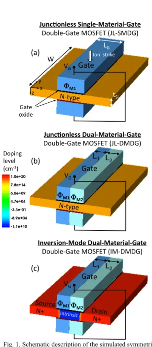
Double-Gate (DG) MOSFET technology is recognized as a promising solution to meet the roadmap requirements in the nanometre scale, mainly due to its excellent control of short channel effects (SCE) ensured by the presence of an additional gate electrode which enhance the potential control of the channel [1-4]. The DG MOSFET technological process can be simplified by using a junctionless (JL) structure [5-7], with the same type of semiconductor throughout the entire silicon film (Fig. 1a). This device has some interesting advantages: there is no doping concentration gradients in the device [8] and the junction leakage currents are totally suppressed, so the off-state current is uniquely controlled by the gate which could be very attractive for ultra-scaled devices. Another interesting concept is to use a dual-material-gate (DM) in order to reduce the hot-carrier effects (HCE) and drain-induced barrier lowering (DIBL) phenomena [9-12]. The junctionless DG MOSFET with dual-material gate (JL-DMDG) has two materials in the gates (Fig. 1b), with different workfunctions, ΦM1 and
ΦM2. This configuration induces a step in the
surface-potential profile which, for ΦM1>ΦM2, simultaneously
provides transconductance increase and DIBL reduction. The step function profile of the surface potential ensures screening of the channel region on the source side (under the material M1) from drain-potential variations. In addition, the electric field peak at the drain is considerably reduced, which suppresses HCEs [13].
Considering the radiation-induced transient effects, simulation studies have been already conducted on junctionless Double-Gate transistors with single-material gate (JL-SMDG, Fig. 1a) and inversion-mode (IM) Double-Gate transistors with either single-material gate (IM-SMDG) or dual-material gate (IM-DMDG, Fig. 1c). These previous studies have shown that IM-SMDG transistors exhibit better radiation immunity than fully-depleted single-gate SOI devices [14-18]. This is ensured by the double-gate structure, which better controls the
N+ VG N-type tSi LG W x y z Doping level (cm-3)
(a)
Ion strike Junc%onless Single-Material-Gate Double-Gate MOSFET (JL-SMDG) Junc%onless Dual-Material-Gate Double-Gate MOSFET (JL-DMDG) Inversion-Mode Dual-Material-Gate Double-Gate MOSFET (IM-DMDG) VG VG Source Drain N+ IntrinsicGate
L1 L2 ΦM1 ΦM2Gate
L1 L2 ΦM1 ΦM2 Gate oxide ΦM1(b)
(c)
Gate
N-typeFig. 1. Schematic description of the simulated symmetrical JL-SMDG, JL-DMDG and IM-DMDG devices. For a better
body potential and reduces the floating body effects. The use of a dual-material-gate in IM-DMDG transistors leads to an enhanced collected charge and higher parasitic bipolar gain than in IM-SMDG counterparts, as shown in [19]. Finally, the behaviour under radiation of junctionless structures has been studied in [20-21] for JL-SMDG devices. This previous works have shown that the high doping level in the film of a JL-SMDG device could have a negative impact on its immunity to single events, because floating body effects are expected to be strong. In spite of its double-gate configuration, JL-SMDG is more sensitive to radiation than IM-SMDG for which the channel is intrinsic. Concerning JL-DMDG, extensive modelling works have been reported in the literature [22-23] in the last years. However, at the best of our knowledge, radiation-sensitivity studies of these devices have not been performed. In this paper we investigate by 3-D numerical simulation the response to single-event of JL-DMDG devices through a detailed comparison with more usual IM-DMDG, IM-SMDG and JL-SMDG transistors. The impact of several technological parameters (such as the length of the high-workfunction material-gate region and the workfunction of the gate material M2) on the single-event transients and the bipolar amplification in JL-DMDG is also addressed.
2. Simulated devices and models
Four devices have been considered in simulation: JL-DMDG, IM-JL-DMDG, JL-SMDG and IM-SMDG. These devices are designed with the same geometrical dimensions: channel length LG=20 nm, 100 nm gate
width, 6 nm-thick silicon film and 1 nm-thick gate oxide, similar to real devices reported in [24]. In junctionless devices, the entire silicon film is uniformly n-type doped at a doping level of 1019 cm-3. In these devices the film
thickness has to be sufficiently small in order to make possible the complete depletion of the silicon film and to be able to cut-off the device [5]. This condition is satisfied for the doping level and the film thickness considered here. The inversion-mode devices (IM-DMDG and IM-SMDG) have an intrinsic channel; source and drain regions are highly n-type doped and the doping profile in these regions is uniform. In single-material gate devices (JL-SMDG and IM-SMDG), a single-material M1 is used for the gates. In dual-material gate devices (JL-DMDG and IM-DMDG) the gates consist of dual materials, M1 (ΦM1) and M2 (ΦM2), of
lengths L1 and L2, respectively (L1+L2=LG). In a first
time we considered L1=L2=LG/2, ΦM1=4.8 eV and
ΦM2=4.1 eV (sections 3 and 4). Next, additional values of
L1 and ΦM2 are considered (section 5).
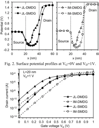
-0.2 0 0.2 0.4 0.6 0.8 1 1.2 1.4 1.6 0 20 40 60 Po te nt ia l (V) x (nm) JL-DMDG JL-SMDG Source Drain -0.2 0 0.2 0.4 0.6 0.8 1 1.2 1.4 1.6 0 20 40 60 Po te nt ia l (V) x (nm) IM-DMDG IM-SMDG Source Drain
Fig. 2. Surface potential profiles at VG=0V and VD=1V.
0 0.1 0.2 0.3 0.4 0.5 0.6 0.7 0.8 0.9 1 D ra in cu rre n t (A) Gate voltage VG (V) JL-DMDG IM-DMDG JL-SMDG IM-SMDG 10-14 10-12 10-8 10-10 10-6 10-4 L=20 nm VD=1 V
Fig. 3. Drain current as function of gate voltage at VD=1V.
3-D numerical simulations have been performed with the DESSIS device simulator from Synopsis Inc. [25]. The main models used in simulation are the Shockley-Read-Hall and Auger recombination models, the Fermi-Dirac carrier statistics and the hydrodynamic model was used for the carrier transport equations. The impact ionization model depends on carrier energy. The mobility model includes the dependence on the carrier energy, lattice temperature and doping level. The ion strike was simulated using the DESSIS HeavyIon module [25]. The electron-hole pair column created in the device by the ion strike is modelled using a carrier-generation function which has a Gaussian radial distribution with a characteristic radius of 20 nm, a Gaussian time distribution, centred on 10 ps and having a characteristic width of 2 ps. In a first time, the ion strikes the device in the channel center (x=30 nm). Other hit locations will be considered in section 4. Devices are biased in the off state (VG=0 V). The drain is constantly
biased at a power supply voltage VD=1 V.
3
. Static characteristicsThe surface potential profiles in junctionless and inversion-mode devices are plotted in Fig. 2. As expected, the surface potential in dual-material-gate
devices has a step-function profile, which is not present for single-material gate devices. This step function profile is responsible of both DIBL reduction and transconductance enhancement. The simulated steady-state drain current characteristics of JL-DMDG, IM-DMDG, JL-SMDG and IM-DMDGare plotted in Fig. 3. Single-material-gate devices have lower off-state current than their dual-material-gate counterparts and near ideal subthreshold swings (63 mV/dec). JL-DMDG device has the highest off-state current but lower subthreshold swing (71 mV/dec) than the IM-DMDG device (83.3 mV/dec). Junctionless devices exhibit lower on-state current than inversion-mode devices because the highly doped silicon film degrades the mobility [17].
4
. Single-Event-Induced Transients4.1. Drain current transient
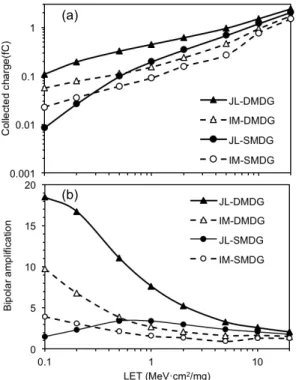
Figure 4 shows the drain current transient resulting from an ion hit in the channel center of the simulated devices, the ion having a linear energy transfer (LET) of 0.1 MeV.cm2/mg. The highest drain current transient peak is obtained for JL-DMDG device. Dual-material-gate transistors have higher transient peaks and wider transients that single-material-gate devices. The reason is probably a higher bipolar gain for dual-material-gate devices due to the step-function profile of the channel potential.
A key parameter of the drain current transient generated by the ion strike is the pulse width. The variation of this parameter is of particular interest for the study of device radiation hardness [26]. The JL-DMDG has a total transient duration of 18.4 ps at 10% of the peak value for LET=1 MeV·cm2/mg (drain current transient not shown). This duration is comparable with that obtained in [20] for JL-SMDG devices where 17.9 ps at 10% of the peak value is found. This value is slightly higher than that obtained in [14] for fully-depleted single-gate SOI devices with 50 nm gate length (15 ps). As reported in [20], the transient duration in JL-DMDG and JL-SMDG is expected to increase with the film doping level. The charge collection is very fast for IM-SMDG and IM-DMDG with a total transient duration of 11.3 ps and 11.9 ps, respectively at LET=1 MeV·cm2/mg. This is essentially due to the intrinsic channel, which limits the floating body effects. 4.2. Collected charge and bipolar amplification
Figures 5a and 5b show the variation of the collected charge (QCOLL) and bipolar amplification as function of
0 0.1 0.2 0.3 0.4 0.5 0.6 0.7 0.8 0 5 10 15 20 25 30 D ra in cu rre nt ( µ A) Time (ps) IM-DMDG JL-SMDG JL-DMDG LET=0.1 MeV.cm2/mg IM-SMDG
Fig. 4. Drain current transients for an ion hit in the center of the channel (LET=0.1 MeV·cm2/mg).
Fig. 5. Collected charge and bipolar amplification as function of LET for an ion hit in the center of the channel.
LET. QCOLL is obtained by integrating the simulated
drain current over the transient duration. The deposited charge, QDEP, is calculated considering the Gaussian
distribution of the ion track and the exact 3-D geometry of the silicon body. The bipolar gain is then given by the ratio between QCOLL and QDEP. The LET range
considered here corresponds to the LET range of a neutron-induced ion in silicon in the terrestrial environment [27-30]. Dual-material-gate devices have higher parasitic bipolar amplification than the single-material-gate counterparts. This can be explained by the reduction of the effective channel length in dual-material-gate devices induced by the presence of a gate
(a)
0 50 100 150 200 0 10 20 30 40 50 60 Pe ak dra in cu rre nt (µ A)
Ion hit location (nm) JL-DMDG
IM-DMDG JL-SMDG IM-SMDG
LET=10 MeV·cm2/mg
Fig. 6. Peak of the drain current transient as a function of the ion hit location (LET=10 MeV.cm2/mg).
material with lower workfunction on the drain side of the gate, which induces a step-function potential profile. Then the collected charge and the bipolar gain values are higher in these devices than those obtained in single-material-gate devices. Concerning the dual-single-material-gate devices, JL-DMDG exhibits a higher bipolar gain than IM-DMDG because of more important floating body effects in the channel of the junctionless device (this device has a higher doping level than the channel of inversion-mode device which is intrinsic). The difference between the four devices is important at low LET, but it gradually weakens when the LET increases. The explanation is that at high LET the electric field is collapsed and then potential variations in the channel have less impact on the parasitic bipolar amplification. The bipolar gain then becomes nearly the same for all devices.
4.3. Device sensitivity to ion hit location
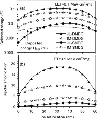
We consider in the following different ion hit locations along the x-axis between the source contact (x=0) and the drain contact (x=60 nm).
The drain current peak (Fig. 6) increase as the ion strike location moves from source to drain with a maximum value at x=40 nm for LET=10 MeV·cm2/mg.
The collected charge and the bipolar gain as a function of the strike location are shown in Fig. 7 for LET=0.1 MeV·cm2/mg and in Fig. 8 for LET=10
MeV·cm2/mg. The deposited charge, Q
DEP, is also
reported for comparison. QDEP is the highest in the
middle of the channel and decreases toward the source and drain sides of the silicon film, because a reduced part of the ion track is contained in the active region [21]. QCOLL has a bell-shaped profile with a maximum around
the middle of the channel and two minima at the source and drain contacts. For all x locations QCOLL is the
highest for JL-DMDG devices. At LET=10 MeV·cm2/mg
0.0001 0.001 0.01 0.1 0 10 20 30 40 50 60 C ol le ct ed ch arg e (f C )
Ion hit location (nm) JL-DMDG IM-DMDG JL-SMDG IM-SMDG LET=0.1 MeV·cm2/mg Deposited charge QDEP (fC)
0 5 10 15 20 0 10 20 30 40 50 60 Bi po la r amp lif ica tio n
Ion hit location (nm) LET=0.1 MeV·cm2/mg
Fig. 7. Collected charge and bipolar gain as a function of the ion hit location for LET=0.1 MeV·cm2/mg.
0 0.5 1 1.5 2 0 10 20 30 40 50 60 C ol le ct ed ch arg e (f C )
Ion hit location (nm) JL-DMDG IM-DMDG JL-SMDG IM-SMDG LET=10 MeV·cm2/mg Deposited charge QDEP (fC) 0 0.5 1 1.5 2 2.5 3 3.5 0 10 20 30 40 50 60 Bi po la r amp lif ica tio n
Ion hit location (nm) JL-DMDG
IM-DMDG JL-SMDG IM-SMDG
LET=10 MeV·cm2/mg
Fig. 8. Collected charge and bipolar gain as a function of the ion hit location for LET=10 MeV·cm2/mg.
and for ion strikes in the source of DMDG and IM-SMDG, QCOLL is lower than QDEP. This indicates that the
bipolar amplification (Fig. 8b) is very low and that there is a strong recombination of the deposited charge in the
(a) (b)
(a)
device [21]. The bipolar gain is always higher JL-DMDG devices than in the three other structures, but has similar dependences on ion hit location for the four structures. For low LET, the bipolar gain maximum is located around the middle of the channel for JL-DMDG and IM-DMDG and at x=40 nm for JL-SMDG and IM-SMDG devices. For LET=10 MeV·cm2/mg, the bipolar
amplification is higher for strikes near the drain region where the electric field is higher. This behavior is consistent with the variation of the bipolar gain obtained in simulation in [19]. The bipolar gain maximum is located at the channel-drain junction in IM-DMDG and IM-SMDG and at x=50 nm for DMDG and JL-SMDG.
5
. Impact of technological parameters on transient response of JL-DMDG devicesWe also investigated the impact of several technological parameters on the transient response of JL-DMDG. This analysis could be useful for the device optimization in terms of geometry and gate material in order to enhance the radiation immunity of JL-DMDG transistors. For all simulations presented in this section we considered that the ion hits in the middle of the channel at x=30 nm.
Firstly, simulations have been performed on dual-material-gate devices with various lengths of the high-workfunction material-gate region, L1, in order to
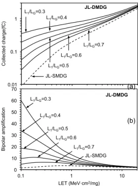
evaluate the impact of this parameter on the transient response of JL-DMDG devices. The variations of the collected charge and the bipolar gain with LET for different ratios L1/LG are reported in Fig. 9. Figure 10
plots the bipolar gain as function of L1. The simulations
of Figs. 9 and 10 are performed for JL-DMDG devices with ΦM1=4.8 eV, ΦM2=4.1 eV and L1+L2=LG. These
simulation results indicate that the collected charge and the bipolar amplification increase when the length of high- workfunction material-gate region is reduced for all LET values. Figure 10 shows that the JL-DMDG structures with L1>0.8×LG have bipolar gains close to
that of the JL-SMDG structure, which is very interesting for obtaining hardened JL-DMDG devices. However, additional investigation is necessary in order to verify if this configuration does not decrease too much the actual performance of these devices en terms of DIBL, short-channel effects and HCE.
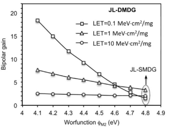
Secondly, simulations have been performed considering JL-DMDG devices including a metal gate M2 with various workfunctions. Figure 11 reports the collected charge as function of LET obtained in JL-DMDG devices with different values of ΦM2 and
0.01 0.1 1 0.1 1 10 C ol le ct ed ch arg e(f C ) LET (MeV·cm2/mg) JL-DMDG JL-SMDG L1/LG=0.3 L1/LG=0.4 L1/LG=0.5 L1/LG=0.7 L1/LG=0.6
0 10 20 30 40 50 60 70 0.1 1 10 Bi po la r amp lif ica tio n LET (MeV·cm2/mg) JL-DMDG JL-SMDG L1/LG=0.5 L1/LG=0.3 L1/LG=0.4 L1/LG=0.7 L1/LG=0.6
Fig. 9. Collected charge and bipolar gain as a function of LET for different ratios L1/LG in JL-DMDG devices. Curves
for JL-SMDG are also reported for comparison (the ion hits at x=30 nm, ΦM1=4.8 eV, ΦM2=4.1 eV). 0 2 4 6 8 10 12 14 0.1 0.2 0.3 0.4 0.5 0.6 0.7 0.8 0.9 1 1.1 Bi po la r ga in L1 / LG JL-DMDG IM-DMDG SMDG
Fig. 10. Bipolar gain as function of L1/LG, for LET=1 MeV·cm2/mg in JL-DMDG devices. 0.01 0.1 1 0.1 1 10 C ol le ct ed ch arg e(f C ) LET (MeV·cm2/mg) JL-DMDG JL-SMDG ΦM2=4.1 eV ΦM2=4.5 eV ΦM2=4.2 eV ΦM2=4.3 eV
Fig. 11. Collected charge as function of LET for different
ΦM2 in JL-DMDG (L1/LG=0.5, ΦM1=4.8 eV). (b) (a)
0 5 10 15 20 4 4.1 4.2 4.3 4.4 4.5 4.6 4.7 4.8 4.9 Bi p o la r g a in Worfunction φM2 (eV) LET=0.1 MeV.cm2/mg LET=1 MeV.cm2/mg LET=10 MeV.cm2/mg JL-DMDG LET=0.1 MeV·cm2/mg LET=1 MeV·cm2/mg LET=10 MeV·cm2/mg JL-SMDG
Fig. 12. Bipolar gain as function of ΦM2, for LET=1 MeV·cm2/mg in JL-DMDG devices (L
1/LG=0.5).
L1=L2=LG/2 (ΦM1=4.8 eV). Results obtained for JL-
SMDG devices are also shown for comparison. At low and intermediate LET values, the simulation results indicate that the collected charge and the bipolar gain (shown in Fig. 12) decrease when ΦM2 is increased. At
high LET (above about 5 MeV·cm2/mg), the transient response become sensibly the same for all devices (JL-DMDG with different ΦM2 and JL-SMDG), because, as
explained before, the high deposited charge collapse the electric field. Then the body-potential differences between the structures have a smaller influence on their transient response. Figure 12 also shows that, at low LET values, increasing ΦM2 substantially reduces the bipolar
gain. This could be interesting for the optimization of JL-DMDG devices in order to minimize single-event transient effects.
6
. ConclusionIn this paper we have analyzed by 3D numerical simulation the transient behavior under radiation of JL-DMDG devices in terms drain current peak, pulse width, collected charge and bipolar gain. A detailed comparison with more conventional devices with single-material-gate or operating in inversion mode has been performed. Our simulation results show that JL-DMDG device has higher parasitic bipolar gain than all other devices. This can be explained by the occurrence of two combined effects: (a) the increase of floating-body effects due to the high-doping level in the film and (b) the reduction of the effective channel length in DMDG owing to the low-workfunction material-gate region, which induces a step-function potential profile. We also have shown that JL-DMDG devices can be optimized in order to reduce the bipolar gain, by increasing the length of the low-workfunction material-gate or/and the low-workfunction of the high-workfunction material-gate region.
References
[1] J.T. Park, J.P. Colinge, Multiple-gate SOI MOSFETs: device design guidelines, IEEE Trans. El. Dev. 49 (2002) 2222-2229.
[2] S. Harrison et al. Electrical characterization and modeling of high-performance SON DG MOSFETs, Proc. European Solid-State Device Research Conference (ESSDERC) 2004, 373–376.
[3] D. Munteanu, J.L. Autran, S. Harrison, J. Non-Cryst. Solids 351 (21–23) (2005) 1911–1918.
[4] D. Munteanu, J.L. Autran, S. Harrison et al., Compact model of the quantum short-channel threshold voltage in symmetric double-gate MOSFET, Mol. Simul. 31 (12) (2005) 831–837.
[5] C.-W. Lee et al., Applied Physics Letters 94 (2009) 053511.
[6] J.P. Colinge et al., Nature Nanotechnology 5 (2010).
[7] J.P. Colinge et al., Reduced electric field in junctionless transistors, Appl. Phys. Lett. 96 (2009) 073510.
[8] A. Kranti, et al., Junctionless Nanowire Transistor (JNT): Properties and Design Guidelines, Proc. European Solid State Device Research Conf. (ESSDERC) 2010, pp. 357–360.
[9] W. Long, H. Ou, J.-M. Kuo, K.K. Chin, IEEE Trans. Electron Devices, vol. 46, no. 5, pp. 865-870, 1999.
[10] G.V. Reddy et al., IEEE Trans. Nanotechn. 4 (2005) 260–268.
[11] M.J. Kumar, A. Chaudhry, Two-dimensional analytical modeling of fully depleted DMG SOI MOSFET and evidence for diminished SCE, IEEE Trans. El. Dev. 15 (2004) 569–574.
[12] M.J. Kumar, G.V. Reddy, Diminished short channel effects in nanoscale double-gate silicon-on-insulator metal oxide field effect transistors due to induced back-gate step potential, Jpn. J. Appl. Phys. 44 (9A) (2005) 6508–6509.
[13] T.K. Chiang, Microelectron. Reliab. 49 (2009) 693-698.
[14] D. Munteanu, V. Ferlet-Cavrois, J.L. Autran et al., Investigation of quantum effects in ultra-thin body single- and double-gate devices submitted to heavy ion irradiation, IEEE Trans. Nucl. Sci. 53 (6) (2006) 3363–3371.
[15] D. Munteanu, J.L. Autran, V. Ferlet-Cavrois et al., 3-D quantum numerical simulation of single-event transients in multiple-gate nanowire MOSFETs, IEEE Trans. Nucl. Sci. 54 (4) (2007) 994–1001.
[16] D. Munteanu, J.L. Autran, Modeling and simulation of single-event effects in digital devices and ICs, IEEE Trans. Nucl. Sci. 55 (4) (2008) 1854–1878.
[17] D. Munteanu, J.L. Autran, 3-D simulation analysis of bipolar amplification in planar DGFET and FinFET with independent gates, IEEE Trans. Nucl. Sci. 56 (4) (2009) 2083–2090.
[18] P. Roche et al., Technology Downscaling Worsening Radiation Effects in Bulk: SOI to the Rescue, IEEE International Electron Device Meeting (IEDM) 2013, 766–769.
[19] D. Munteanu, J.L. Autran, 3D Simulation of Single-Event-Transient Effects in Symmetrical Dual-Material Double-Gate MOSFETs, Microelectron. Reliab. 55 (2015) 1522-1526.
[20] D. Munteanu, J.L. Autran, 3-D numerical simulation of bipolar amplification in junctionless DG MOSFETs under heavy-ion irradiation, IEEE Trans. Nucl. Sci. 59 (2012) 773–780.
[21] D. Munteanu, J.L. Autran, Radiation sensitivity of junctionless double-gate 6T SRAM cells investigated by 3-D numerical simulation, Microelectron. Reliab. 54 (2009) 2284-2288.
[22] J. Singh et al., IEEE Trans. El. Dev. 63 (6) (2016) 2282-2287.
[23] P. Wang et al., Jpn. J. Appl. Phys. 53 (8) (2014) 084201.
[24] M. Vinet et al., Bonded Planar Double-Metal-Gate NMOSFET Down to 10 nm, IEEE Electron Dev. Lett., 26 (2005) 317-319.
[25] Synopsys Sentaurus TCAD tools, Available online: http://www.synopsys.com/products/tcad/tcad.html.
[26] P. E. Dodd et al., Production and propagation of single-event transients in high-speed digital logic ICs, IEEE Trans. Nucl. Sci. 51 (6) (2004) pp. 3278–3284.
[27] Y.P. Fang et al., Neutron-induced charge collection simulation of bulk FinFET SRAMs compared with conventional planar SRAMs, IEEE Trans. Device Mater. Reliab. 11 (2011) 551–554.
[28] J.L. Autran et al., Altitude and underground real-time SER characterization of CMOS 65 nm SRAM, IEEE Trans. Nucl. Sci. 56 (4) (2009) 2258–2266.
[29] J.L. Autran, D. Munteanu, Soft Errors: From Particles to Circuits, Taylor & Francis/CRC Press, 2015.
[30] J.L. Autran et al., Soft-errors induced by terrestrial neutrons and natural alpha-particle emitters in advanced memory circuits at ground level, Microelectron. Reliab. 50 (2010) 1822–183.