HAL Id: hal-03065804
https://hal.archives-ouvertes.fr/hal-03065804
Submitted on 15 Dec 2020
HAL is a multi-disciplinary open access
archive for the deposit and dissemination of sci-entific research documents, whether they are pub-lished or not. The documents may come from teaching and research institutions in France or abroad, or from public or private research centers.
L’archive ouverte pluridisciplinaire HAL, est destinée au dépôt et à la diffusion de documents scientifiques de niveau recherche, publiés ou non, émanant des établissements d’enseignement et de recherche français ou étrangers, des laboratoires publics ou privés.
Ge(Sn) growth on Si(001) by magnetron sputtering
H. Khelidj, A. Portavoce, M. Bertoglio, M. Descoins, L. Patout, K.
Hoummada, A. Hallén, A. Charaï, M.C. Benoudia, D. Mangelinck
To cite this version:
H. Khelidj, A. Portavoce, M. Bertoglio, M. Descoins, L. Patout, et al.. Ge(Sn) growth on Si(001) by magnetron sputtering. Materials Today Communications, Elsevier, 2020, pp.101915. �10.1016/j.mtcomm.2020.101915�. �hal-03065804�
Ge(Sn) growth on Si(001) by magnetron sputtering
H. Khelidj1,2, A. Portavoce1,*, M. Bertoglio1, M. Descoins1, L. Patout1, K. Hoummada1, A. Hallén3, A. Charaï1, M. C. Benoudia2, and D. Mangelinck1
1IM2NP, CNRS/Aix-Marseille University, Faculté des Sciences de Saint-Jérôme case 142, 13397 Marseille, France 2
Ecole Nationale Supérieure des Mines et de la Métallurgie, L3M, Annaba, Algeria
3KTH, Royal Institute of Technology, School of Electrical Engineering and Computer Science (EECS), SE-164 40 Kista-Stockholm, Sweden
ABSTRACT
The semi-conductor Ge1xSnx exhibits interesting properties for optoelectronic
applications. In particular, Ge1xSnx alloys with x 0.1 exhibit a direct band-gap, and integrated
in complementary-metal-oxide-semiconductor (CMOS) technology, should allow the development of Si photonics. CMOS-compatible magnetron sputtering deposition was shown to produce monocrystalline Ge1xSnx films with good electrical properties at low cost. However,
these layers were grown at low temperature (< 430 K) and contained less than 6% of Sn. In this work, Ge1xSnx thin films were elaborated at higher temperature (> 600 K) on Si(001) by
magnetron sputtering in order to produce low-cost and CMOS-compatible relaxed pseudo-coherent layers with x ≥ 0.1 exhibiting a better crystallinity. Ge1xSnx crystallization and Ge1xSnx
crystal growth were investigated. Crystallization of an amorphous Ge1xSnx layer deposited on
Si(001) or Ge(001) grown on Si(001) leads to the growth of polycrystalline films. Furthermore, the competition between Ge/Sn phase separation and Ge1xSnx growth prevents the formation of
large-grain Sn-rich Ge1xSnx layers without the formation of -Sn islands on the layer surface,
due to significant atomic redistribution kinetics at the crystallization temperature (T = 733 K for x = 0.17). However, the growth at T = 633 K of a highly-relaxed pseudo-coherent Ge0.9Sn0.1 film
magnitude smaller than undoped Ge is demonstrated. Consequently, magnetron sputtering appears as an interesting technique for the integration of optoelectronic and photonic devices based on Ge1xSnx layers in the CMOS technology.
Keywords: GeSn, Magnetron Sputtering, Silicon substrate, Epitaxy
*
1. Introduction
Current microelectronic device production is based on the complementary-metal-oxide-semiconductor (CMOS) technology [1-2]. This technology has significantly evolved over the years due to device size reduction requirements and partly relies on thin film deposition, growth, and patterning capabilities at the nanometer scale [3]. It is currently based on Silicon (Si) and Germanium (Ge) semiconductors and their alloys, as well as on the use of different metals (Cu, Ni, Pt…), oxides (SiO2, HfO2…) and nitrides (Si3N4, TiN…) [4-8]. This technology provides a
high production rate of cost-effective integrated nanostructured devices with high levels of purity and reliability. Photonics is a well-established technology allowing for high speed communication [9-10]. However, the integration of photonic devices and circuits in microelectronic chips would promote the development of new optoelectronic technologies, boosting the capacity of current electronic devices [11-14]. Standard CMOS technology already allows the integration of photonic devices such as waveguides (Si nitrides), SiGe-based optical modulators, and Ge- or SiGe-based photodetectors [15-19].However, Si and Ge being indirect band-gap semiconductors, an essential photonic element is missing for full integrated CMOS Si-photonic development: a light source (i.e. laser integration). Ge1xSnx is a CMOS-compatible
IV-IV semiconductor exhibiting interesting properties for infrared photodetector, light emitting diode, and laser fabrication [20-26]. Furthermore, Ge1xSnx alloys can be used for the fabrication
of integrated optical amplifier, Gas sensors [27], and high-speed thin-film transistors [28-29], and direct band-gap Ge1xSnx alloys are of high interest for solar cells [30]. Ge1xSnx single crystals
are expected to be best suited for all these applications, since grain boundaries (GB) in polycrystalline films create deep band-gap levels and act as effective recombination centers, and impair device efficiency. For example, the electronic behavior of polycrystalline semiconductors
is strongly dependent on grain size. GB scattering decreases charge carrier mobility, which can increase linearly with grain size at constant temperature [28]. In the case of p-doped Ge, an inversion from p-type to n-type can be observed if the trap energy level in GB lies in the upper half of the band-gap [31].
The Ge1xSnx alloy is expected to exhibit a direct band-gap for Sn compositions of 10 at%
(x = 0.1) and above, as required for laser fabrication [32-34]. However, the maximum Sn solubility limit in Ge is ~ 1.1 at % at 673 K [35-36]. Consequently, only metastable Sn-rich Ge1xSnx layers can be produced [37]. The microcrystalline, optical and electrical properties of
Ge1xSnx films may consequently be highly dependent on fabrication techniques and conditions.
Furthermore, the large difference of lattice parameters between Si and Ge1xSnx alloys increases
growth complexity, the lattice parameter of diamond Sn being 19.5% larger than the Si lattice parameter [38]. Semiconductor growth is usually performed using chemical vapor deposition (CVD) [39] or molecular beam epitaxy (MBE) [40], to produce defect-free and contamination-free layers, compatible with microelectronic technology requirements. The sputtering technique is CMOS-compatible and significantly low-cost compared to the CVD and MBE techniques [41]. However, sputtered layers are expected to be highly contaminated, in particular with O and C, and to exhibit poor electrical properties compared to layers grown by MBE or CVD. Si1xGex
layers are currently grown by CVD in the CMOS technology [42-43], while magnetron sputtering is used for ohmic contact fabrication for example [44-45]. However, high quality Ge1xSnx
material can be obtained by sputtering: Ge1xSnx-based photodetectors using a Ge0.94Sn0.06 active
layer grown by sputtering were shown to exhibit a dark-current density and a responsivity comparable with similar devices using MBE-grown Ge1xSnx layers [46]. The growth of Ge1xSnx
layers directly sputtered on an Si(001) substrate are usually polycrystalline [47-49], but monocrystalline sputtered Ge1xSnx layers can be grown on Ge(001) and GaAs(001) substrates,
using low growth temperatures between 423 and 443 K [50-51]. Zheng et al. [52] succeeded to grow Ge1xSnx single crystals on Si(001) substrates using the growth of a sputtered Ge buffer on
the Si substrate before Ge1xSnx deposition. The Ge buffer was grown at T = 673 K, but the
Ge1xSnx film was grown at T = 423 K with x 0.06. Ge1xSnx films grown or annealed at higher
temperatures generally exhibit better crystal quality and thus better electrical properties [53]. Low temperature growth is necessary to ensure Sn incorporation. CVD or MBE growths of Ge1xSnx
are usually performed at temperatures comprised between 473 and 723 K, and the obtained films are sometimes annealed at higher temperatures in order to improve the electrical and optical properties [54-55].
The indirect-to-direct band gap transition occurring at lower Sn composition for relaxed Ge1xSnx films [56-58], the present work aims to investigate the low-cost high-temperature
growth of relaxed monocrystalline Ge1xSnx films on Si(001) with x 0.1 in a commercial
magnetron sputtering setup. Indeed, relaxed Ge0.9Sn0.1 films were grown at T = 633 K in
pseudo-epitaxy on Si(001) using magnetron sputtering. These films contain impurity concentrations lower than 2 × 10¹⁹ at cm3 and exhibit an electrical resistivity four orders of magnitude lower than that of undoped Ge.
2. Experiments
Ge and Sn were co-deposited on Si(001) substrates using a 99.9999% pure Ar gas flow to simultaneously sputter in DC mode a 99.999% pure Ge target and a 99.99% pure Sn target, in a commercial magnetron sputtering system exhibiting a base pressure of 10−8 Torr. In this setup,
the sample is mounted on a horizontal rotating sample holder, and three targets can be placed symmetrically (120° angle between each target) above the sample, with an angle of 45° between the normals of the target surfaces and the sample surface. Deposition was performed at the pressure of 2.25 103 Torr. The sample was rotating at a speed of 5 rpm and was set to ground level, while a voltage was applied to each target to maintain a constant power during deposition. The Ge target was sputtered at the power of 15 W during the deposition of the Ge buffer, corresponding to a deposition rate of 0.09 nm s1. Ge1xSnx was deposited during 96 s with a
power of 150 W for the Ge target and a power of 15 W for the Sn target, corresponding to a deposition rate of 0.84 nm s1 for Ge and of 0.21 nm s1 for Sn. The Ge and Sn fluxes were calibrated separately, using X-ray reflectivity to determine the thicknesses of sputtered films deposited at room temperature (RT) in different conditions. In the following, the nominal composition of the films, i.e. calculated from the Ge and Sn fluxes taking into account the atomic volume difference between Ge and Sn ( Sn/Ge ~ 1.2), will be given unless otherwise specified.
The Si substrates were dipped in a 5% HF solution in order to remove the Si native oxide before being loaded in the growth chamber. The structure of the Ge1xSnx films was studied by X-ray
diffraction (XRD) in the Bragg-Brentano geometry (−) using a Cu K source (K = 0.154 nm) in a PANalytical X’Pert PRO setup equipped with an X’Celerator detector designed for high speed data collection. This setup was also used to perform in situ XRD measurements during amorphous Ge1xSnx film crystallization. In this case, the temperature was raised from 423 to
853 K following a heating ramp made of 5 K per minute steps separated by 5 min long XRD measurements at constant temperature, corresponding to an average heating ramp of 1 K min1. Structural observations were also performed using transmission electron microscopy (TEM). Scanning TEM Dark-Field (STEM-DF) and Energy Dispersive X-Ray Spectrometry (EDS)
analyses were acquired at 200 keV using a LaB6 Thermo Fisher Tecnai TEM equipped with a
silicon drift detector OXFORD X-max80. High-Resolution TEM images were performed at 200 keV using a field emission gun Thermo Fisher Titan microscope equipped with a spherical aberration (Cs) correction system. We consider the Cs value in an order of magnitude between 0 and 0.05 mm allowing a point-to-point resolution around 1 Å to be reached. The surface topography of the layers was studied using scanning electron microscopy (SEM) and atomic force microscopy (AFM). AFM images were obtained in non-contact mode using a PSIA XE-100 in air microscope. The composition of the layers was determined using Rutherford backscattering (RBS) and atom probe tomography (APT). For the RBS, 2.0 MeV alpha particles were used with a backscatter detector positioned at 170°. SEM images as well as the TEM and APT sample preparations were performed in an FEI dual beam HELIOS 600 nanolab setup. APT measurements were performed at T = 50 K using a laser-pulsed CAMECA LEAP 3000XHR microscope, with a laser pulse frequency of 100 kHz and a laser power of 0.2 nJ. The resistivity of the films was measured at RT by the four probe method.
3. Results and discussion
3.1. Ge(Sn) Crystallization
FIG. 1. a) XRD measurements performed during the in
situ annealing of an amorphous Ge0.83Sn0.17 film
deposited on Si(001), following an average ramp of ~ 1 K min1 from 423 to T = 853 K; and b) diffractogram acquired at T = 778 K during the in situ annealing (red line in a).
Fig. 1a presents in situ XRD measurements recorded during annealing a 100 nm-thick Ge0.83Sn0.17 film deposited at room temperature on Si(001). No diffraction peaks are observed
after deposition, the film being amorphous. Three diffraction peaks at 2 = 26.92°, 44.70°, and 52.87° appear simultaneously during the annealing ramp, when the temperature reaches T = 733 K. They respectively correspond to the atomic planes (111), (220), and (311) of the Ge1xSnx
diamond structure (fig. 1b). Surprisingly, one can note that their intensity decreases when the temperature increases, and the peaks disappear concurrently, leaving no diffraction signal at T = 853 K.
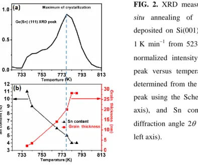
FIG. 2. XRD measurements performed during the in
situ annealing of an amorphous Ge0.83Sn0.17 film
deposited on Si(001), following an average ramp of ~ 1 K min1 from 523 to T = 853 K: a) integrated and normalized intensity of the Ge1xSnx(111) diffraction
peak versus temperature, and b) average grain size determined from the half-maximum width of the (111) peak using the Scherrer equation (solid squares, right axis), and Sn concentration determined from the diffraction angle 2 of the (111) peak (solid triangles, left axis).
Fig. 2a shows the intensity variation of the (111) peak recorded during the annealing ramp. The peak is detected at T = 733 K and its intensity increases with temperature up to T = 778 K. This stage corresponds to the nucleation followed by the growth of the Ge1xSnx crystal from the initial
amorphous film. For temperatures higher than T = 778 K, the intensity of the (111) diffracted peak decreases and finally disappears at T = 818 K, without the apparition of other diffraction peaks until the end of the annealing at T = 873 K. In order to understand this behavior, the variations of the full width at half maximum (FWHM) of the (111) peak were analyzed using the Scherrer equation, giving the average grain size in the direction perpendicular to the film surface
[59]. The “thickness” variations versus temperature of the Ge1xSnx grains with (111) planes
oriented parallel to the film surface are shown in fig. 2b (solid squares, right axis). The data should be interpreted qualitatively since parameters other than grain size could also modify the FWHM of diffraction peaks. However, one can note that the grain size is significantly smaller than the film thickness. The grain size is less than 3 nm when the diffraction peak is first detected, and increases with temperature to reach a maximum size of about 30 nm at T = 783 K,
in agreement with the nucleation and growth of the Ge1xSnx polycrystalline film up to this
temperature. The size of the Ge1xSnx grains stays constant after T = 783 K, despite the decrease
of the diffraction peak intensity (fig. 2a). The variations of the diffraction angle 2 of the (111) peak were investigated considering the polycrystalline Ge1xSnx layer fully relaxed, and its lattice
parameter aGeSn following the corrected-Vegard law:
(1)
aGe = 0.565 nm, aSn = 0.649 nm, and b = 0.0041 nm are respectively the Ge and Sn lattice
parameters in the diamond structure, and the bowing coefficient [48-60]. The average Sn content of the crystalized Ge1xSnx layer was deduced from this equation, using the Bragg equation [61]
and the experimental diffraction angle 2 to determine aGeSn. Fig. 2b presents the variation of the
Sn concentration in the Ge1xSnx grains versus temperature. The Sn concentration is about 11% at
the beginning of crystallization, and continuously decreases as temperature increases, reaching 4% before the disappearance of the diffraction peak. Ge1xSnx crystallization at 733 K allowed Sn
incorporation above 10% to be obtained. However, atom mobility is fast enough to support Ge and Sn phase separation at this temperature and above. As expected, the in situ XRD measurements reveal a strong competition between Sn incorporation and Ge1xSnx crystallization.
As soon as the nucleation process is completed, the crystal growth rate as well as the Ge/Sn separation rate increase with temperature. One can note that the grain size and their Sn composition stay almost constant while the diffraction peak intensity decreases. This phenomenon can be explained by a lateral shrinking of the 30 nm-thick Ge0.96Sn0.04 grains. Since
diffraction peak, meaning that either its grains exhibit crystallographic orientations not compatible with the - diffraction geometry, or the phase is actually amorphous or liquid.
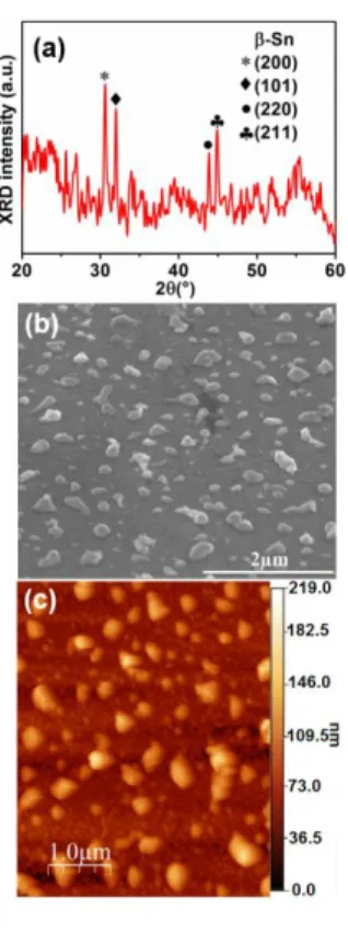
FIG. 3. Analyses performed at RT on the sample that experienced the XRD in situ annealing presented in Fig. 1 and 2: a) X-ray diffractogram, b) SEM measurements, and c) AFM measurements.
Fig. 3a shows the diffractogram measured on the sample at RT after the ramp annealing. Diffraction peaks corresponding to β-Sn are detected. Thus, the Ge1xSnx phase was probably
consumed by the growth of liquid Sn, as the Sn bulk melting temperature is ~ 505 K and can be lower for nanocrystals [62]. However, no diffraction peak corresponding to crystalline Ge is detected at RT, suggesting that the mechanism of Ge/Sn phase separation at high temperature in the thin film leads to the formation of amorphous Ge. Fig. 3b and 3c present SEM and AFM images of the sample surface after annealing. Large islands are observed with a lateral size between 94 and 470 nm, an average height ~ 110 nm, and a surface density ~ 8.4 × 108 cm2. The root-mean-square (RMS) surface roughness is ~ 26 nm. These islands probably correspond to the Sn-rich phase that crystallized during sample cooling. Fig. 4 presents STEM Dark-Field observations performed on the sample after the in situ XRD annealing. Fig. 4a shows a
cross-section view between two islands similar to that observed on the sample surface by SEM (Fig. 3b) and AFM (Fig. 3c). The Pt layer was deposited on the sample surface for TEM sample preparation. The islands are in direct contact with the Si substrate, as confirmed by High-Resolution TEM observations (Fig. 4b). One can note that the island/Si interface is flat and abrupt, which suggest that this interface corresponds to the initial Si substrate surface.
FIG. 4. Cross-section TEM measurements performed on the sample that experienced the XRD in situ annealing presented in Fig. 1 and 2: a) STEM Dark-Field image, b) and c) High-Resolution TEM images. The inset in c) presents the local FFT obtained on the layer A.
This is in agreement with the Si-Sn phase diagram [35], showing phase separation between Si and Sn. The maximum solubility of Sn in Si is 0.1 at% at 1339 K, while the solubility limit of Si in -Sn is less than 0.5 at%. The stack of two layers (noted A and B in Fig. 4a) is observed between the two islands. Fig. 4c presents a High-Resolution TEM image of the interface between these two layers. The layer A is amorphous and its average thickness is ~ 25 nm. As shown in the inset of Fig. 4c, a short-range order exists in the layer, corresponding to a distance of 0.32 nm (radius of the ring in the FFT pattern in the inset), which is significantly higher than the nearest neighbor distance (~ 0.245 nm) in the Ge crystal. Below this amorphous layer, a bright contrast is observed with an average thickness of ~ 30 nm, corresponding to the layer B. Fig. 4c shows that this layer is crystalline and coherent with the Si crystal. EDS analyses (not shown) confirmed that
the islands contain only Sn atoms (in the detection limit of the technique). However, the overlapping of Ge and Pt signals prevented the Ge distribution in the sample to be determined. The TEM observations show that the mechanism of Ge/Sn phase separation is complex. Sn atoms are located in large islands exhibiting a height similar to the thickness of the amorphous Ge0.83Sn0.17 layer initially deposited on Si (Fig. 4a). However, the Ge atoms seem to have been
incorporated in the Si Substrate, part in an amorphous layer and part in the Si lattice, as the bright contrast of the layer B can be due to the presence in this region of atoms heavier than Si. Ge evaporation from the Si substrate and Ge lattice diffusion in Si cannot occur at 853 K. However, Sn migration in Ge is effective at this temperature, Sn atoms living the Ge1xSnx film to form
liquid Sn droplets. Thus, Ge evaporation from the surface of melted Sn cannot be ruled out. According to Ge self-diffusion [63-64], Ge atom mobility is limited at 853 K (few nanometers after one hour), which can be the reason for the Ge layer to stay amorphous once emptied of the Sn atoms. The Ge/Si intermixing located in the layer B is difficult to explain considering equilibrium kinetic parameters such as lattice diffusion. This intermixing could occur only through short-circuit paths, such as interface diffusion/redistribution, or due to unusual high concentrations of point defects. XRD in situ isothermal annealing at T = 788 K was performed on the same as-deposited Ge0.83Sn0.17 film. The thermal annealing was stopped as soon as Ge1xSnx
FIG. 5. Diffractograms measured at RT on an amorphous Ge0.83Sn0.17 film deposited on the native
silicon oxide formed on Si(001) and annealed at T = 788 K for 6 min, before (top) and after (bottom) chemical etching in a 5% HF solution (a), and SEM images obtained on the same sample before (b) and after (c) chemical etching.
Fig. 5a shows the diffractogram (top) measured at RT on this sample after annealing. The diffraction peaks (111), (220), and (311) of the Ge1xSnx crystal are observed, as well as two
diffraction peaks (not observed at T = 788 K) at 2 = 30.70°, and 32.06°, corresponding to -Sn(200) and -Sn(101), respectively. These peaks are detected at the diffraction angle of pure -Sn, indicating that the Ge content in the crystallized Sn islands should not be above the (relatively low) Ge solubility in Sn. The average Sn concentration in the Ge1xSnx grains is ~ 6%
and the average grain size is ~ 18 nm from the XRD analysis. Fig. 5b presents an SEM image of the sample surface. A network of connected islands is observed. The sample was dipped in a 5% HF solution to remove the Sn-rich alloy located on the surface of the sample, before XRD measurements at RT (bottom diffractogram in fig. 5a) [65]. The diffraction peaks of the
Ge0.94Sn0.06 film are still detected after etching, but the diffraction peaks of -Sn have
disappeared. SEM images of the surface after etching (fig. 5c) show a flat surface with holes exhibiting lateral sizes between 19 and 160 nm, with a surface density ~ 2.7 109 cm2.
FIG. 6. AFM measurements performed on the same sample as in Fig. 5c, after annealing at T = 788 K for 6 min and chemical etching in a 5% HF solution: a) surface topography, and b) 1D topography profile along the blue line shown in a).
AFM measurements (fig. 6) give an RMS surface roughness ~ 1.3 nm, and an average lateral grain size ~ 25 nm, which is in agreement with the Ge1xSnx grain size determined from the XRD
peaks, considering the lateral inaccuracy involved with AFM in air due to tip effects. Obviously, these holes correspond to the locations of the -Sn(Ge) alloy and confirm that the Ge/Sn phase separation process should occur laterally in the layer, with the formation of a liquid -Sn(Ge) alloy, probably developing droplets on the Ge1xSnx surface.
These results show that the atomic mobility and the Ge/Sn phase separation kinetic are too high at the Ge1xSnx crystallization temperature to easily obtain large-grain Sn-rich
The limiting phenomenon is probably nucleation, since crystalline Ge1xSnx layers can be grown
at lower temperatures.
3.2. Ge buffer growth
As reported in the literature, Ge1xSnx layers deposited on Si are usually polycrystalline.
However, monocrystalline Ge1xSnx layers can be grown on Si substrate using the deposition of a
Ge buffer on the Si substrate before the growth of the Ge1xSnx layer.
FIG. 7. X-ray diffractograms measured at RT on a 100 nm-thick Ge film deposited at RT on the Si(001) substrate and annealed at 873 K for 30 min (top) and a 100 nm-thick Ge film deposited on Si(001) at T = 633 K (bottom).
Fig. 7 presents the diffractogram measured at RT on a 100 nm-thick Ge layer deposited at RT on the Si(001) substrate and annealed at 873 K for 30 min under vacuum (P < 106 mbar). The Ge layer is polycrystalline as the (111), (220), and (311) diffraction peaks of the Ge diamond structure are detected at 2 = 27.29°, 45.54°, and 53.82°, respectively. One can note that the polycrystalline Ge film exhibits the same peaks and the same peak intensity ratios as the polycrystalline Ge1xSnx films that are characteristics of a randomly oriented polycrystal with a
diamond structure (Si, Ge, Ge1xSnx…). Indeed, thin film growth is highly dependent on surface
and interface energies, and the surface and interface contributions in the overall film energy increases as the film thickness decreases. Depending on atom mobility during growth (growth
conditions), the film tends to exhibit a texture allowing for energy minimization, as much as possible. The {111} and {113} surfaces are known to be low-energy surfaces of the diamond structure, while {110} facets are more easily observed on surfaces exhibiting low-level contamination of O and C. {111} and {113} facets are the equilibrium facets of relaxed Si and Ge crystals [66] and are observed on relaxed Si-Ge islands [67-68]. Consequently, if the surface contamination level stays low, the texture of polycrystalline Si, Ge and Ge1xSnx films generally
shows a large fraction of grains exhibiting the {111} and {113} crystallographic orientations in the direction parallel to the film surface. The relaxed Ge lattice parameter arel is expected to be ~
0.565 nm at RT [69]. In the - XRD geometry used in this study, the measured plane spacing corresponds to plane spacing in the direction perpendicular to the film surface and is thus denoted dexp. The Ge film lattice parameter in the direction perpendicular to the surface aexp was thus
determined from the diffraction angles of the three diffraction peaks Ge(111), Ge(220), and Ge(311) using the Bragg equation. In average aexp = 0.565 nm, corresponding to a fully relaxed Ge polycrystalline layer. The Si lattice parameter was also determined from the Si(400) diffraction peak observed in the same diffractogram (fig. 7) for comparison. For the Si substrate aexp = 0.543 nm, as expected for relaxed Si [70].
The crystallization of a Ge layer deposited at RT on the Si(001) substrate cannot be used for growing a monocrystalline Ge1xSnx film, since it leads to the formation of a polycrystalline
Ge buffer. Instead, the Ge buffer should be grown at a sufficiently high temperature to allow the Ge crystal to form in partial coherence with the Si substrate due to a high enough atomic mobility, but sufficiently low to prevent extensive Si/Ge intermixing and interdiffusion. Note that the epitaxy is only partially coherent because of the large thickness of the Ge layer and the large misfit between Si and Ge that lead to the nucleation of misfit dislocations. Fig. 7 shows XRD
measurements (bottom diffractogram) performed at RT on a 100 nm-thick Ge layer deposited by magnetron sputtering on Si(001) at T = 633 K. This diffractogram corresponds to a Ge layer that is pseudo-coherent with the Si substrate: a single Ge diffraction peak is now observed at 2 = 65.98°, corresponding to the same orientation as the substrate Si(400) diffraction peak. RBS measurements (not shown) confirmed that the layer contains only Ge and that its thickness is ~ 100 nm. XRD measurements give aexp = 0.566 nm, which indicates that the Ge layer is
compressively strained on the Si substrate [71]. Considering that arel = 0.565 nm for Ge, the
perpendicular distortion exp of this pseudo-coherent Ge layer was found to be exp = 0.0018,
using eq. 2 [72].
(2)
Considering that the Poisson’s ratio of Ge ~ 0.271 [72], the parallel distortion //exp of the Ge
lattice was determined using eq. 3 [73].
(3)
//exp = 0.0024 corresponding to a//exp = 0.564 nm (eq. 2), and thus, corresponding to a relative
relaxation rate R = 95.5% (eq. 4).
The Ge film is significantly relaxed and should contain a high concentration of dislocations [52-62, 64-74].
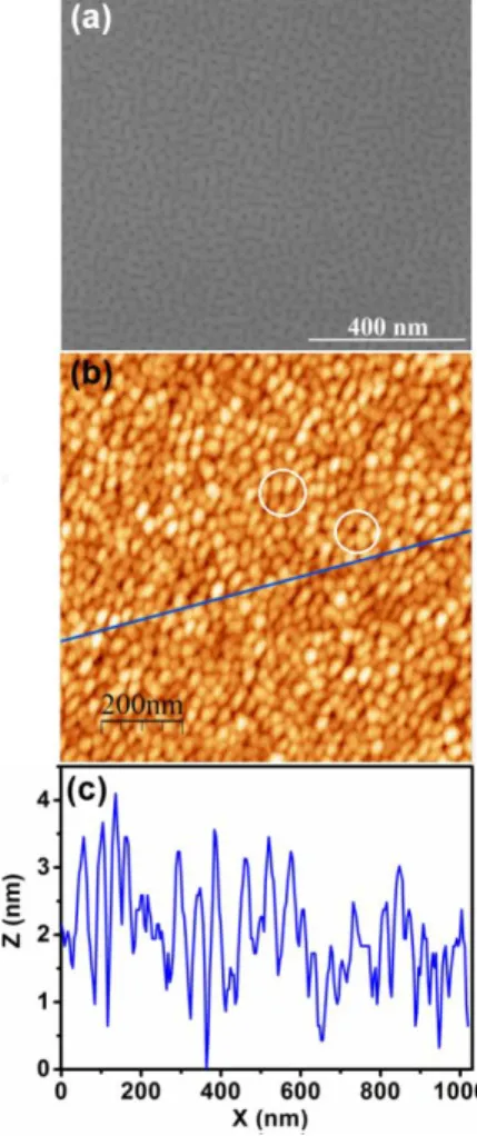
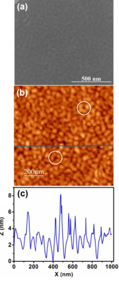
Fig. 8a presents an SEM image of the Ge layer surface. A structure made of undulations in quasi-perpendicular directions is observed. Each squared structure seems to be surrounding a depression (hole?) in the layer, with a surface density ~ 1.2 1011 cm2. This structure is more difficult to observe in AFM images acquired on the same sample (fig. 8b). AFM images show circular and elongated islands with typical sizes (length × width) of (100 nm × 25 nm).
FIG. 8. Measurements performed on the surface of a 100 nm-thick Ge film deposited at T = 633 K on Si(001): a) SEM image, b) AFM image, and c) AFM profile measured along the line presented in b).
The height of these islands varies typically between 1 and 3 nm (fig. 8c), and the RMS of the surface is ~ 0.71 nm, which are significantly smaller than the thickness of the film. Similar to the
SEM images, depressions (~ 3 nm) surrounded by three to five islands are also observed (white circle in fig. 8b). The surface structure displayed in the SEM and AFM images has been also observed by Zhang et al. [75] on the surface of Sn-rich Ge1xSnx layers grown by MBE on
Ge(001) substrates at T = 473 K. They interpreted this surface structure as the formation of Sn islands on the Ge1xSnx layer surface due to Ge/Sn phase separation. However, in our case, the
same structure is found on the surface of the pure Ge buffer, and thus cannot be attributed to Sn. This structure should be related to stress relaxation through elastic and plastic relaxation mechanisms. For example, similar surface states can be observed on Si(Ge) layers grown in epitaxy on Si(001) [73-76]. The layers studied by Zhang et al. were shown to be partially relaxed and to contain threading dislocations. Considering the high relaxation level of the Ge layer, this structure should be related to both the weak residual epitaxial stress located in the film, and threading dislocations. In the case of Sn-rich Ge1xSnx layers with low residual strain grown by
low-pressure CVD on a Ge buffer grown on Si(001), Nicolas et al. [77] showed thanks to APT measurements that quasi-vertical dislocation lines are passing through the Ge1xSnx layer up to
the surface. The depressions observed on the film surface could correspond to similar dislocations reaching the surface and locally modifying the elastic strain, promoting the formation of several island-like ripples around the end of the dislocation line. In this case, the density of the surface depressions (1.2 1011 cm2) should correspond to the threading dislocation density in the Ge buffer. The presence of a surface structure on a buffer layer is not desired, as this structure may prevent the epitaxial growth of a following film and can promote the formation of structural defects at the buffer/film interface. However, in the present case, the surface roughness of the Ge buffer is very low (~ 5 Ge atomic steps in the (001) direction), and
such a Ge buffer can be used as virtual substrate to grow pseudo-coherent Sn-rich Ge1xSnx
layers, as reported in the case of CVD and MBE growth [54-62, 65-74].
3.3. Ge(Sn) single crystal growth
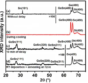
Fig. 9 presents X-ray diffractograms measured at RT on different 100 nm-thick Ge0.83Sn0.17 films grown on the Ge buffer in different conditions. The diffractogram (a)
corresponds to a Ge0.83Sn0.17 film deposited at the same temperature as the Ge buffer without
growth interruption. The chosen growth temperature T = 633 K is 100 K lower than the Ge0.83Sn0.17 crystallization temperature determined in the XRD in situ ramp annealing
experiments (T = 733 K), aiming to increase Sn incorporation, but is 200 K higher than the growth temperature used in former studies (T = 423 K) for growing Ge0.94Sn0.06 layers by
sputtering, aiming to improve the layer crystalline properties. This temperature is actually in the range used to grow Sn-rich Ge1xSnx layers by CVD or MBE.
FIG. 9. X-ray diffractograms measured at RT on different 100 nm-thick Ge0.83Sn0.17 films grown in
different conditions on a 100 nm-thick Ge buffer grown at T = 633 K on Si(001): a) deposition at the same temperature as the Ge buffer without growth interruption, b) deposition without growth interruption but stopping sample heating before Ge0.83Sn0.17
deposition, c) deposition after stopping sample heating at the end of the Ge buffer deposition and with a growth interruption of 10 min before Ge0.83Sn0.17 deposition, and
d) crystallization of an amorphous Ge0.83Sn0.17 film
The (004) diffraction peak is the only one corresponding to the diamond structure detected for the Si substrate, as well as for the Ge and Ge1xSnx layers, displaying the pseudo-coherent relation
between the substrate and the two stacked layers. However, one can note that the Ge1xSnx(400)
diffraction peak is less intense than that of the Ge(400). A small diffraction peak corresponding to -Sn(101) is also detected, meaning that Sn droplets are probably present on the sample surface (Fig. 3). The formation of the phase -Sn can be suppressed using a modified growth process consisting of switching off the sample heater before growing the Ge1xSnx layer, without
growth interruption between the Ge buffer and the Ge1xSnx layer. In this case, XRD
measurements (diffractogram (b) in Fig. 9) show no sign of the -Sn phase, and the Ge1xSnx(400) and Ge(400) diffraction peak intensities are similar. The diffractogram (c) shown
in Fig. 9 was acquired on a sample for which the sample heater was switched off after the growth of the Ge buffer and a growth interruption of 10 min was performed before Ge1xSnx growth. The
-Sn phase is not detected in this case, but the Ge1xSnx(400) peak intensity is smaller than the
Ge(400) peak intensity, and additional Ge1xSnx diffraction peaks are observed, corresponding to
the three diamond lattice orientations (111), (220), and (311), usually detected for Ge and Ge1xSnx layers crystallized from an amorphous layer deposited on Si(001) (Figs. 1b, 5a, and 7).
Obviously, the Ge1xSnx layer grew in pseudo-epitaxy on the Ge buffer at the beginning, but due
to the temperature decrease, the end of the Ge1xSnx growth promoted the formation of a
polycrystalline layer. However, according to the significant difference of diffraction peak intensity, the top polycrystalline layer should be significantly thinner than the monocrystalline layer in contact with the Ge buffer. The last diffractogram (d) in Fig. 9 was acquired after the crystallization of an amorphous Ge0.83Sn0.17 film deposited at RT on the Ge buffer. In this case,
the Ge buffer is pseudo-coherent with the Si(001) substrate, but the Ge1xSnx film is entirely
polycrystalline and the Ge1xSnx(400) peak characteristic of epitaxial growth is not detected.
As expected, the growth of a pseudo-coherent Ge1xSnx layer on Si(001) without the
formation of the -Sn phase is highly dependent on kinetics, and growth conditions generally need to be determined empirically. Fig. 10 shows SEM and AFM measurements performed on the surface of the Ge1xSnx layer coherently grown on the Ge buffer (diffractogram (b) in Fig. 9).
FIG. 10. Analyses performed on the surface of a 100 nm-thick Ge0.83Sn0.17 film deposited on a 100 nm-thick
Ge buffer grown at T = 633 K on Si(001) in the conditions corresponding to Fig. 9b (no growth interruption, sample heater off): a) SEM image, b) AFM image, and c) AFM profile measured along the line presented in b).
A surface structure is observed similar to that displayed on the Ge buffer before Ge1xSnx
deposition, in agreement with the observations of Zhang et al. [75]. The pattern is less organized than that on the Ge buffer surface. The ripples/islands exhibit a similar average height ~ 3 nm (Fig. 10c), but they are larger with an average width ~ 75 nm (Figs. 10a and 10b). The RMS of
the surface is ~ 1.24 nm. One can note that 3 nm-high islands on the Ge surface should have been easily covered with the 100 nm-thick Ge1xSnx layer. The fact that this topography is also
observed on the Ge1xSnx surface is thus in agreement with the effect of extended defects, such as
dislocations, which can propagate in the Ge1xSnx layer from its pseudo-coherent interface with
the Ge buffer up to the surface. The surface density of the depressions surrounded with islands is reduced to ~ 3.3 1010 cm2 on the Ge1xSnx surface. Consequently, the Ge1xSnx layer may
contain a threading dislocation density almost one order of magnitude smaller than that of the Ge buffer. This might be related to the lower misfit between Ge1xSnx and Ge (about 1.5%) than
between Ge and Si (about 4%).
However, the precise determination of the misfit requires knowledge of the composition of Sn in Ge1xSnx. Fig. 11a presents the Sn and Ge atomic distributions determined by APT in the
Ge1xSnx layer. The Sn and Ge distributions (solid symbols) follow random distributions (solid
lines), and are centered on 10 at% and 90 at% for Sn and Ge, respectively. Thus, the film corresponds to a Ge0.9Sn0.1 solid solution free of Sn clusters. Interestingly, no contaminants are
detected in the Ge0.9Sn0.1 layer. Indeed, Fig. 11b shows part of the mass spectrum corresponding
FIG. 11. Chemical characterization of the 100 nm-thick Ge0.83Sn0.17 film deposited on a 100 nm-thick Ge buffer
grown at T = 633 K on Si(001) in the conditions corresponding to Fig. 9b (no growth interruption, sample heater off): a) Ge and Sn atomic distributions determined by APT in the Ge1xSnx layer (solid
symbols) compared to random distribution (solid lines) centered on 90 and 10 at%, respectively, b) part of the mass spectrum acquired by APT in the Ge1xSnx layer,
and d) RBS measurements performed on the same sample (black) and simulations (red solid line) corresponding to the structure 100 nm-thick Ge0.0Sn0.1
/100 nm-thick Ge /Si(001).
The impurities C and O usually incorporated in sputtered layers are not detected, meaning that their concentrations are lower than 2 × 10¹⁹ at cm3 (~ 0.04 at%) in the film [78]. The Sn composition determined by APT is in agreement with RBS measurements performed on the same sample (Fig. 11c). Furthermore, the RBS measurements are consistent with the stack of a 100 nm-thick Ge0.9Sn0.1 layer and a 100 nm-thick Ge layer on the Si substrate. However, one can
note that the Sn concentration of this film is significantly lower than that of the expected Ge0.83Sn0.17 film, corresponding to Ge and Sn fluxes used during growth. Since no Sn cluster was
detected by APT in the Ge0.9Sn0.1 layer, this lack of Sn should be mainly due to Sn desorption
from the sample surface during growth. Indeed, the growth was performed at a temperature about 100 K higher than the Sn bulk melting temperature, at a pressure P ~ 3 × 10⁻³ mbar of Ar. The lattice parameter of the Ge0.9Sn0.1 layer in the direction perpendicular to the sample surface was
diffractogram (b) in Fig. 9. Considering that a0.1GeSn = 0.574 nm (eq. 1), the perpendicular
distortion of the Ge0.9Sn0.1 lattice parameter was found to be exp = 0.0035 (eq. 2).
(5)
According to eq. 5 [72], the Poisson’s ratio of Ge0.9Sn0.1 is 0.1GeSn = 0.280 (Ge = 0.271 and Sn =
0.360 [72]), leading to //exp = 0.0045 (eq. 3) and a//exp = 0.571 nm (eq. 2). Consequently, the
relative relaxation rate of the Ge0.9Sn0.1 film compared to that of the Si substrate is R = 90.3%
(eq. 4). The Ge0.9Sn0.1 film is significantly relaxed, but not as relaxed as the Ge buffer, which is
in agreement with a lower dislocation density in the Ge0.9Sn0.1 layer. The resistivity of the
undoped Ge0.9Sn0.1 film was measured at RT. It was found to be 0.1GeSn = 8 × 104 cm. For
comparison, the resistivity of undoped monocrystalline Ge at RT is Ge ~ 50 cm [79].
Despite the unusual deposition technique employed for semiconductor growth, and the significant threading dislocation density probably contained in the layers, the resistivity of the Ge0.9Sn0.1 film is found to be four orders of magnitude lower than that of Ge. Magnetron
sputtering can be used to grow a pseudo-coherent Ge0.9Sn0.1 film on Si(001) at a relatively high
temperature (T = 633 K), displaying a high level of relaxation (R = 90.3%) and relatively low impurity concentrations (< 2 × 10¹⁹ at cm3), exhibiting interesting electrical properties (0.1GeSn =
8 × 104 cm).
4. Conclusion
Magnetron sputtering growth of Ge1xSnx layers (x > 0.6) on Si(001) was performed at
clearly evidenced the competition between Sn incorporation and crystal growth. The high crystallization temperature of Ge1xSnx, compared to the atomic diffusion kinetic and to the Sn
melting temperature, drastically limits the fabrication of crystalline Sn-rich Ge1xSnx films.
Furthermore, the crystallization of an amorphous Ge1xSnx layer deposited directly on a clean
Si(001) substrate, or on a Ge buffer grown on the Si(001) substrate, does not allow the growth of a pseudo-coherent Ge1xSnx layer, probably due to crystal nucleation starting at the surface of the
amorphous Ge1xSnx layer instead of at the Ge1xSnx /Si(001) or Ge1xSnx /Ge(001) interface. The
Ge buffer and the Ge1xSnx layer must be grown at a temperature allowing for crystal growth and
dislocation nucleation without significant atomic transport, in order to grow a monocrystalline layer without Ge/Sn phase separation. This temperature can be significantly lower than the Ge1xSnx crystallization temperature, as the nucleation process is unnecessary when the layers are
grown on a single crystal. The low-cost and CMOS-compatible magnetron sputtering technique can be used to grow, at similar temperature as for CVD or MBE growth, relaxed Sn-rich Ge1xSnx
layers with x ≥ 0.1, displaying low impurity concentrations and reasonable electrical properties. While Sn incorporation is mainly limited by Ge/Sn phase separation kinetics during Ge1xSnx
crystallization, Sn surface desorption appears as the main limiting phenomenon during growth at temperatures lower than the crystallization temperature.
Acknowledgements
This work was supported by the French-Algerian cooperation program PROFAS B+. The Ion Technology Centre ITC, Uppsala University, Sweden, is acknowledged for the RBS facilities.
References
[1] J. W. Jeong et al., “Tunnelling-based ternary metal–oxide–semiconductor technology,” Nat. Electron., vol. 2, no. 7, pp. 307–312, Jul. 2019, doi: 10.1038/s41928-019-0272-8.
[2] A. L. Robinson, “CMOS Future for Microelectronic Circuits: Low power consumption of complementary metal-oxide-semiconductor integrated circuits drives next stage of
ultraminiaturization,” Science, vol. 224, no. 4650, pp. 705–707, May 1984, doi: 10.1126/science.224.4650.705.
[3] P. Arunkumar, S. K. Kuanr, and K. S. Babu, “Thin Film: Deposition, Growth Aspects, and Characterization,” in Thin Film Structures in Energy Applications, S. Babu Krishna
Moorthy, Ed. Cham: Springer International Publishing, 2015, pp. 1–49.
[4] R. Pillarisetty, “Academic and industry research progress in germanium nanodevices,” Nature, vol. 479, no. 7373, pp. 324–328, Nov. 2011, doi: 10.1038/nature10678. [5] C. Chang, “Formation of copper silicides from Cu(100)/Si(100) and Cu(111)/Si(111)
structures,” J. Appl. Phys., vol. 67, no. 1, pp. 566–569, Jan. 1990, doi: 10.1063/1.345194. [6] D. Mangelinck et al., “Three-dimensional composition mapping of NiSi phase distribution
and Pt diffusion via grain boundaries in Ni2Si,” Scr. Mater., vol. 62, no. 8, pp. 568–571, Apr. 2010, doi: 10.1016/j.scriptamat.2009.12.044.
[7] B. Radisavljevic, A. Radenovic, J. Brivio, V. Giacometti, and A. Kis, “Single-layer MoS 2 transistors,” Nat. Nanotechnol., vol. 6, no. 3, pp. 147–150, Mar. 2011, doi:
10.1038/nnano.2010.279.
[8] Yee-Chia Yeo et al., “Dual-metal gate CMOS technology with ultrathin silicon nitride gate dielectric,” IEEE Electron Device Lett., vol. 22, no. 5, pp. 227–229, May 2001, doi:
10.1109/55.919237.
[9] T. Nagatsuma, G. Ducournau, and C. C. Renaud, “Advances in terahertz communications accelerated by photonics,” Nat. Photonics, vol. 10, no. 6, pp. 371–379, Jun. 2016, doi: 10.1038/nphoton.2016.65.
[10] Y. A. Vlasov, “Silicon CMOS-integrated nano-photonics for computer and data
communications beyond 100G,” IEEE Commun. Mag., vol. 50, no. 2, pp. s67–s72, Feb. 2012, doi: 10.1109/MCOM.2012.6146487.
[11] O. Graydon, “The data centre challenge,” Nat. Photonics, vol. 9, no. 10, pp. 637–638, Oct. 2015, doi: 10.1038/nphoton.2015.186.
[12] G. T. Reed, G. Mashanovich, F. Y. Gardes, and D. J. Thomson, “Silicon optical modulators,” Nat. Photonics, vol. 4, no. 8, pp. 518–526, Aug. 2010, doi:
10.1038/nphoton.2010.179.
[13] M. Hochberg and T. Baehr-Jones, “Towards fabless silicon photonics,” Nat. Photonics, vol. 4, no. 8, pp. 492–494, Aug. 2010, doi: 10.1038/nphoton.2010.172.
[14] X. Chen, C. Li, and H. K. Tsang, “Device engineering for silicon photonics,” NPG Asia Mater., vol. 3, no. 1, pp. 34–40, Jan. 2011, doi: 10.1038/asiamat.2010.194.
[15] M. Cazzanelli et al., “Second-harmonic generation in silicon waveguides strained by silicon nitride,” Nat. Mater., vol. 11, no. 2, pp. 148–154, Feb. 2012, doi: 10.1038/nmat3200.
[16] C. Lacava et al., “Si-rich Silicon Nitride for Nonlinear Signal Processing Applications,” Sci. Rep., vol. 7, no. 1, pp. 1–13, Feb. 2017, doi: 10.1038/s41598-017-00062-6.
[17] Y. Kim, M. Takenaka, T. Osada, M. Hata, and S. Takagi, “Strain-induced enhancement of plasma dispersion effect and free-carrier absorption in SiGe optical modulators,” Sci. Rep., vol. 4, no. 1, pp. 1–6, Apr. 2014, doi: 10.1038/srep04683.
[18] J. Michel, J. Liu, and L. C. Kimerling, “High-performance Ge-on-Si photodetectors,” Nat. Photonics, vol. 4, no. 8, pp. 527–534, Aug. 2010, doi: 10.1038/nphoton.2010.157.
[19] I. Stavarache et al., “SiGe nanocrystals in SiO 2 with high photosensitivity from visible to short-wave infrared,” Sci. Rep., vol. 10, no. 1, pp. 1–9, Feb. 2020, doi: 10.1038/s41598-020-60000-x.
[20] H. Cong et al., “Silicon Based GeSn p-i-n Photodetector for SWIR Detection,” IEEE Photonics J., vol. 8, no. 5, pp. 1–6, Oct. 2016, doi: 10.1109/JPHOT.2016.2607687.
[21] M. Oehme et al., “GeSn Heterojunction LEDs on Si Substrates,” IEEE Photonics Technol. Lett., vol. 26, no. 2, pp. 187–189, Jan. 2014, doi: 10.1109/LPT.2013.2291571.
[22] A. Elbaz et al., “Ultra-low-threshold continuous-wave and pulsed lasing in tensile-strained GeSn alloys,” Nat. Photonics, pp. 1–8, Mar. 2020, doi: 10.1038/s41566-020-0601-5. [23] S. Ghosh et al., “Metal-Semiconductor-Metal GeSn Photodetectors on Silicon for
Short-Wave Infrared Applications,” Micromachines, vol. 11, no. 9, p. 795, Aug. 2020, doi: 10.3390/mi11090795.
[24] K. Choe, M. R. Hogsed, N. Miguel, J. W. McClory, and J. Kouvetakis, “Displacement Damage Effects in Germanium Tin LEDs,” vol. 38, no. 1, p. 8, 2020.
[25] Y. Zhou et al., “Optically Pumped GeSn Lasers Operating at 270 K with Broad Waveguide Structures on Si,” ACS Photonics, vol. 6, no. 6, pp. 1434–1441, Jun. 2019, doi:
10.1021/acsphotonics.9b00030.
[26] A. Elbaz et al., “Reduced Lasing Thresholds in GeSn Microdisk Cavities with Defect Management of the Optically Active Region,” ACS Photonics, p. acsphotonics.0c00708, Sep. 2020, doi: 10.1021/acsphotonics.0c00708.
[27] K. P. Homewood and M. A. Lourenço, “The rise of the GeSn laser”, Nature Photon., Vol. 9, pp. 78-79, February 2015, doi: 10.1038/nphoton.2015.1.
[28] K. Moto, R. Yoshimine, T. Suemasu, K. Toko, “Imptoving carrier mobility of polycrystalline Ge by Sn doping”, Sci. Rep., vol. 8, p. 14832, October 2018, doi: 10.1038/s41598-018-33161-z.
[29] C. Xu, X. Gong, M. Miyao, and T. Sadoh, “Enhanced mobility of Sn-doped Ge thin-films (≤50 nm) on insulator for fully depleted transistors by nucleation-controlled solid-phase crystallization,” Appl. Phys. Lett., vol. 115, no. 4, p. 042101, Jul. 2019, doi:
10.1063/1.5096798.
[30] Roucka et al. patent US2014/0053894A1, Feb. 2014.
[31] H. J. Möller and V. Schlichting, “Measurement and calculation of the carrier concentration in polycrystalline germanium thin films”, Springer Proc. Phys., vol. 35, pp. 326-331, 1989. [32] S. Wirths et al., “Lasing in direct-bandgap GeSn alloy grown on Si,” Nat. Photonics, vol. 9,
no. 2, pp. 88–92, Feb. 2015, doi: 10.1038/nphoton.2014.321.
[33] J. Song, X. Zhao, X. Wu, and R. Xuan, “High rectification efficiency direct bandgap
Ge1−xSnx Schottky diode for microwave wireless power transfer,” Appl. Phys. A, vol. 125, no. 10, p. 719, Sep. 2019, doi: 10.1007/s00339-019-3002-1.
[34] S. Prucnal et al., “Ex situ n$\mathplus$ doping of GeSn alloys via non-equilibrium processing,” Semicond. Sci. Technol., vol. 33, no. 6, p. 065008, May 2018, doi: 10.1088/1361-6641/aabe05.
[35] “Binary Alloy Phase Diagrams, 2nd Edition - ASM International.”
https://www.asminternational.org/online-catalog/alloy-phase-diagrams/-/journal_content/56/10192/57718G/PUBLICATION (accessed Apr. 29, 2020).
[36] R. W. Olesinski and G. J. Abbaschian, “The Ge−Sn (Germanium−Tin) system,” Bull. Alloy Phase Diagr., vol. 5, no. 3, pp. 265–271, Jun. 1984, doi: 10.1007/BF02868550.
[37] H. Groiss et al., “Free-running Sn precipitates: an efficient phase separation mechanism for metastable Ge 1−x Sn x epilayers,” Sci. Rep., vol. 7, no. 1, pp. 1–12, Nov. 2017, doi: 10.1038/s41598-017-16356-8.
[38] “KittelCharles-IntroductionToSolidStatePhysics8ThEd.pdf.” .
[39] S. d. Allen, “Laser chemical vapor deposition: A technique for selective area deposition,” J. Appl. Phys., vol. 52, no. 11, pp. 6501–6505, Nov. 1981, doi: 10.1063/1.328600.
[40] M. B. Panish, “Molecular Beam Epitaxy,” Science, vol. 208, no. 4446, pp. 916–922, May 1980, doi: 10.1126/science.208.4446.916.
[41] S. Lee et al., “Fabrication of high-quality single-crystal Cu thin films using radio-frequency sputtering,” Sci. Rep., vol. 4, no. 1, pp. 1–6, Aug. 2014, doi: 10.1038/srep06230.
[42] R. Xu, W. Li, J. He, K.-C. Qi, and Y.-D. Jiang, “Structural and photoelectronic properties of a-SiGe:H thin films with varied Ge prepared by PECVD,” in 2011 Asia Communications and Photonics Conference and Exhibition (ACP), Nov. 2011, pp. 1–7, doi:
10.1117/12.904214.
[43] D. Zhang, L. Jin, Y. Liao, H. Zhang, and J. Kolodzey, “Microstructure and optic-electric performance of SiGe/Si heterostructures,” in 2016 IEEE International Nanoelectronics Conference (INEC), May 2016, pp. 1–2, doi: 10.1109/INEC.2016.7589384.
[44] M. Mysliwiec, M. Sochacki, R. Kisiel, M. Guziewicz, and M. Wzorek, “TiAl-based ohmic contacts on p-type SiC,” in Proceedings of the 2011 34th International Spring Seminar on Electronics Technology (ISSE), May 2011, pp. 68–72, doi: 10.1109/ISSE.2011.6053552. [45] K. Buchholt et al., “Ohmic contact properties of magnetron sputtered Ti3SiC2 on n- and
p-type 4H-silicon carbide,” Appl. Phys. Lett., vol. 98, no. 4, p. 042108, Jan. 2011, doi: 10.1063/1.3549198.
[46] J. Zheng et al., “GeSn p-i-n photodetectors with GeSn layer grown by magnetron sputtering epitaxy,” Appl. Phys. Lett., vol. 108, no. 3, p. 033503, Jan. 2016, doi: 10.1063/1.4940194. [47] L. Zhang et al., “Raman scattering study of amorphous GeSn films and their crystallization
on Si substrates,” J. Non-Cryst. Solids, vol. 448, pp. 74–78, Sep. 2016, doi: 10.1016/j.jnoncrysol.2016.07.007.
[48] H. Mahmodi, M. R. Hashim, and U. Hashim, “Formation of nanocrystalline GeSn thin film on Si substrate by sputtering and rapid thermal annealing,” Superlattices Microstruct., vol. 98, pp. 235–241, Oct. 2016, doi: 10.1016/j.spmi.2016.08.030.
[49] H. Mahmodi, M. Hashim, T. Soga, S. Alrokayan, H. Khan, and M. Rusop, “Synthesis of Ge1−xSnx Alloy Thin Films by Rapid Thermal Annealing of Sputtered Ge/Sn/Ge Layers on Si
Substrates,” Materials, vol. 11, no. 11, p. 2248, Nov. 2018, doi: 10.3390/ma11112248. [50] H. P. Ladr n de Guevara, A. G. Rodr guez, H. Navarro-Contreras, and M. A. Vidal,
“Ge1−xSnx alloys pseudomorphically grown on Ge(001),” Appl. Phys. Lett., vol. 83, no. 24, pp. 4942–4944, Dec. 2003, doi: 10.1063/1.1634374.
[51] L. Qian et al., “GeSn/GaAs Hetero-Structure by Magnetron Sputtering,” IEEE J. Quantum Electron., vol. 56, no. 2, pp. 1–5, Apr. 2020, doi: 10.1109/JQE.2019.2963057.
[52] J. Zheng et al., “Growth of Crystalline Ge1−xSnx Films on Si (100) by Magnetron
Sputtering,” ECS Solid State Lett., vol. 3, no. 9, p. P111, Jul. 2014, doi: 10.1149/2.0081409ssl.
[53] N. Taoka et al., “Electrical and optical properties improvement of GeSn layers formed at high temperature under well-controlled Sn migration,” Mater. Sci. Semicond. Process., vol. 57, pp. 48–53, Jan. 2017, doi: 10.1016/j.mssp.2016.09.040.
[54] B. R. Conley et al., “Temperature dependent spectral response and detectivity of GeSn photoconductors on silicon for short wave infrared detection,” Opt. Express, vol. 22, no. 13, pp. 15639–15652, Jun. 2014, doi: 10.1364/OE.22.015639.
[55] X. Zhang et al., “Crystal Quality Improvement of GeSn Alloys by Thermal Annealing,” ECS Solid State Lett., vol. 3, no. 10, p. P127, Aug. 2014, doi: 10.1149/2.0101410ssl. [56] S. A. Ghetmiri et al., “Direct-bandgap GeSn grown on silicon with 2230 nm
photoluminescence,” Appl. Phys. Lett., vol. 105, no. 15, p. 151109, Oct. 2014, doi: 10.1063/1.4898597.
[57] T. T. Tran et al., “Ion beam synthesis and photoluminescence study of supersaturated fully-relaxed Ge-Sn alloys,” Mater. Sci. Eng. B, vol. 262, p. 114702, Dec. 2020, doi:
10.1016/j.mseb.2020.114702.
[58] T. T. Tran et al., “Ion beam synthesis and photoluminescence study of supersaturated fully-relaxed Ge-Sn alloys,” Mater. Sci. Eng. B, vol. 262, p. 114702, Dec. 2020, doi:
10.1016/j.mseb.2020.114702.
[59] U. Holzwarth and N. Gibson, “The Scherrer equation versus the ‘Debye-Scherrer equation,’” Nat. Nanotechnol., vol. 6, no. 9, pp. 534–534, Sep. 2011, doi:
10.1038/nnano.2011.145.
[60] F. Gencarelli et al., “Crystalline Properties and Strain Relaxation Mechanism of CVD Grown GeSn,” ECS J. Solid State Sci. Technol., vol. 2, no. 4, p. P134, Jan. 2013, doi: 10.1149/2.011304jss.
[61] M. Kim et al., “Polycrystalline GeSn thin films on Si formed by alloy evaporation,” Appl. Phys. Express, vol. 8, no. 6, p. 061301, May 2015, doi: 10.7567/APEX.8.061301.
[62] M. Liu and R. Y. Wang, “Size-Dependent Melting Behavior of Colloidal In, Sn and Bi Nanocrystals,” Sci. Rep., vol. 5, no. 1, pp. 1–9, Nov. 2015, doi: 10.1038/srep16353.
[63] A. Portavoce, O. Abbes, Y. Rudzevich, L. Chow, V. Le Thanh, C. Girardeaux, "Manganese diffusion in monocrystalline germanium", Scripta Mater., vol. 67, pp. 269–272, May 2012, doi: 10.1016/j.scriptamat.2012.04.038.
[64] A. Chroneos and H. Bracht, “Diffusion of n-type dopants in germanium”, Appl. Phys. Rev., vol. 1, p. 011301, January 2014, doi: 10.1063/1.4838215.
[65] K. Toko, N. Oya, N. Saitoh, N. Yoshizawa, and T. Suemasu, “70 °C synthesis of high-Sn content (25%) GeSn on insulator by Sn-induced crystallization of amorphous Ge,” Appl. Phys. Lett., vol. 106, no. 8, p. 082109, Feb. 2015, doi: 10.1063/1.4913744.
[66] J.M. Bermond, J.J. Métois, X. Egéa, F. Floret, “The equilibrium shape of silicon”, Surface Science, vol. 330, pp. 48-60, 1995, SSD1 0039-6028(95)00230-8
[67] A. Portavoce, A. Ronda, I. Berbezier, “Sb-surfactant mediated growth of Ge
nanostructures”, Mat. Sci. Eng. B, vol. 89, pp. 205–210, 2002, PII: S0921-5107(01)00853-4.
[68] A. Portavoce, R. Hull, M. C. Reuter, M. Copel, and F. M. Ross, “Control of homoepitaxial Si nanostructures by locally modified surface reactivity”, Appl. Phys. Lett., vol. 92, p. 053106, Feb. 2008, doi: 10.1063/1.2841673.
[69] Yu. G. Sadofyev, V. P. Martovitsky, M. A. Bazalevsky, A. V. Klekovkin, D. V. Averyanov, and I. S. Vasil’evskii, “Ge/GeSn heterostructures grown on Si (100) by molecular-beam epitaxy,” Semiconductors, vol. 49, no. 1, pp. 124–129, Jan. 2015, doi:
10.1134/S1063782615010248.
[70] P. Moontragoon, R. A. Soref, and Z. Ikonic, “The direct and indirect bandgaps of unstrained SixGe1−x−ySny and their photonic device applications,” J. Appl. Phys., vol. 112, no. 7, p. 073106, Oct. 2012, doi: 10.1063/1.4757414.
[71] S. Wirths et al., “Tensely strained GeSn alloys as optical gain media,” Appl. Phys. Lett., vol. 103, no. 19, p. 192110, Nov. 2013, doi: 10.1063/1.4829360.
[72] J. Aubin et al., “Impact of thickness on the structural properties of high tin content GeSn layers,” J. Cryst. Growth, vol. 473, pp. 20–27, Sep. 2017, doi:
10.1016/j.jcrysgro.2017.05.006.
[73] I. Berbezier, A. Ronda, and A. Portavoce, “SiGe nanostructures: new insights into growth processes,” J. Phys. Condens. Matter, vol. 14, no. 35, pp. 8283–8331, Aug. 2002, doi: 10.1088/0953-8984/14/35/306.
[74] S. Takeuchi, Y. Shimura, O. Nakatsuka, S. Zaima, M. Ogawa, and A. Sakai, “Growth of highly strain-relaxed Ge1−xSnx/virtual Ge by a Sn precipitation controlled compositionally step-graded method,” Appl. Phys. Lett., vol. 92, no. 23, p. 231916, Jun. 2008, doi:
10.1063/1.2945629.
[75] Z. P. Zhang et al., “Structural properties of GeSn thin films grown by molecular beam epitaxy,” AIP Adv., vol. 7, no. 4, p. 045211, Apr. 2017, doi: 10.1063/1.4982245. [76] F. Volpi, A. Portavoce, A. Ronda, Y. Shi, J. M. Gay, and I. Berbezier, “Nucleation and
evolution of Si1−xGex islands on Si(001),” Thin Solid Films, vol. 380, no. 1, pp. 46–50, Dec.
2000, doi: 10.1016/S0040-6090(00)01526-1.
[77] J. Nicolas, S. Assali, S. Mukherjee, A. Lotnyk, and O. Moutanabbir, “Dislocation pipe diffusion and solute segregation during the growth of metastable GeSn”, Cryst. Growth Des., Apr. 2020, doi: 10.1021/acs.cgd.0c00270.
[78] M. Descoins, J. Perrin Toinin, S. Zhiou, K. Hoummada, M. Bertoglio, R. Ma, L. Chow, D. Narducci, A. Portavoce, "PdGe contact fabrication on Se-doped Ge", Scripta Mater., vol. 139, pp. 104-107, June 2017, doi: 10.1016/j.scriptamat.2017.06.029.
[79] L. H. Chan, E. I. Altman, and Y. Liang, “Development of procedures for obtaining clean, low-defect-density Ge(100) surfaces,” J. Vac. Sci. Technol. A, vol. 19, no. 3, pp. 976–981, May 2001, doi: 10.1116/1.1367264.
FIGURE CAPTIONS
FIG. 1. a) XRD measurements performed during the in situ annealing of an amorphous
Ge0.83Sn0.17 film deposited on Si(001), following an average ramp of ~ 1 K min1 from 423 to T =
853 K; and b) diffractogram acquired at T = 778 K during the in situ annealing (red line in a).
FIG. 2. XRD measurements performed during the in situ annealing of an amorphous Ge0.83Sn0.17
film deposited on Si(001), following an average ramp of ~ 1 K min1 from 523 to T = 853 K: a) integrated and normalized intensity of the Ge1xSnx(111) diffraction peak versus temperature, and
b) average grain size determined from the half-maximum width of the (111) peak using the Scherrer equation (solid squares, right axis), and Sn concentration determined from the diffraction angle 2 of the (111) peak (solid triangles, left axis).
FIG. 3. Analyses performed at RT on the sample that experienced the XRD in situ annealing
presented in Fig. 1 and 2: a) X-ray diffractogram, b) SEM measurements, and c) AFM measurements.
FIG. 4. Cross-section TEM measurements performed on the sample that experienced the XRD in
situ annealing presented in Fig. 1 and 2: a) STEM Dark-Field image, b) and c) High-Resolution TEM images. The inset in c) presents the local FFT obtained on the layer A.
FIG. 5. Diffractograms measured at RT on an amorphous Ge0.83Sn0.17 film deposited on the
after (bottom) chemical etching in a 5% HF solution (a), and SEM images obtained on the same sample before (b) and after (c) chemical etching.
FIG. 6. AFM measurements performed on the same sample as in Fig. 5c, after annealing at T =
788 K for 6 min and chemical etching in a 5% HF solution: a) surface topography, and b) 1D topography profile along the blue line shown in a).
FIG. 7. X-ray diffractograms measured at RT on a 100 nm-thick Ge film deposited at RT on the
Si(001) substrate and annealed at 873 K for 30 min (top) and a 100 nm-thick Ge film deposited on Si(001) at T = 633 K (bottom).
FIG. 8. Measurements performed on the surface of a 100 nm-thick Ge film deposited at T =
633 K on Si(001): a) SEM image, b) AFM image, and c) AFM profile measured along the line presented in b).
FIG. 9. X-ray diffractograms measured at RT on different 100 nm-thick Ge0.83Sn0.17 films grown
in different conditions on a 100 nm-thick Ge buffer grown at T = 633 K on Si(001): a) deposition at the same temperature as the Ge buffer without growth interruption, b) deposition without growth interruption but stopping sample heating before Ge0.83Sn0.17 deposition, c) deposition after
stopping sample heating at the end of the Ge buffer deposition and with a growth interruption of 10 min before Ge0.83Sn0.17 deposition, and d) crystallization of an amorphous Ge0.83Sn0.17 film
FIG. 10. Analyses performed on the surface of a 100 nm-thick Ge0.83Sn0.17 film deposited on a
100 nm-thick Ge buffer grown at T = 633 K on Si(001) in the conditions corresponding to Fig. 9b (no growth interruption, sample heater off): a) SEM image, b) AFM image, and c) AFM profile measured along the line presented in b).
FIG. 11. Chemical characterization of the 100 nm-thick Ge0.83Sn0.17 film deposited on a 100
nm-thick Ge buffer grown at T = 633 K on Si(001) in the conditions corresponding to Fig. 9b (no growth interruption, sample heater off): a) Ge and Sn atomic distributions determined by APT in the Ge1xSnx layer (solid symbols) compared to random distribution (solid lines) centered on 90
and 10 at%, respectively, b) part of the mass spectrum acquired by APT in the Ge1xSnx layer,
and d) RBS measurements performed on the same sample (black) and simulations (red solid line) corresponding to the structure 100 nm-thick Ge0.0Sn0.1 /100 nm-thick Ge /Si(001).
Khelidj et al.
Khelidj et al. Figure 2
Khelidj et al. Figure 3
Khelidj et al. Figure 4
Khelidj et al. Figure 5
Khelidj et al. Figure 6
Khelidj et al. Figure 7
Khelidj et al. Figure 8
Khelidj et al. Figure 9
Khelidj et al. Figure 10
Khelidj et al Figure 11