CMOS Circuits for VCSEL-Based Optical IO
by
Alexandra M. Kern
Bachelor of Arts in Engineering Sciences
Dartmouth College, 2002
Bachelor of Engineering in Electrical Engineering
Dartmouth College, 2002
Master of Science in Electrical Engineering and Computer Science
Massachusetts Institute of Technology, 2004
Submitted to the Department of Electrical Engineering and Computer
Science
in Partial Fulfillment of the Requirements for the Degree of
Doctor of Philosophy
at the
MASSACHUSETTS INSTITUTE OF TECHNOLOGY
June 2007
@ 2007 Massachusetts Institute of Technology
All Rights Reserved
Author ...
...
Department of Electrical Engineering and Computer Science
A
March 28, 2007
C ertified by ...
Anantha P. Chandrakasan
Professor of Eleineerinputer
Science
Accepted by ... .. , ....
Arthur C. Smith
MASSAC-HU•ET'1
OFTECHNOILOy
Chairman
.LIBRARIES
, Department Committee on Graduate Students
'CMOS Circuits for VCSEL-Based Optical IO
by
Alexandra M. Kern
Submitted to the Department of Electrical Engineering and Computer Science on March 28, 2007, in partial fulfillment of the
requirements for the degree of Doctor of Philosophy
Abstract
Electrical IO is becoming limited by copper interconnect channel losses that depend on frequency and distance. Package-to-package optical interconnects see negligible frequency-dependent channel losses, but data rates are limited by the intrinsic op-tical dynamics and electrical parasitics of the opop-tical devices. This thesis presents 90nm CMOS front-end circuits which apply techniques to operate optical components beyond the intrinsic data rates imposed by these bandwidth limits.
The differential TIA is based on a proposed core amplifier which uses cross-coupled NMOS cascodes to increase gain and bandwidth. A symmetric feedback method provides constant gain from DC to 9GHz. The TIA operates at 12.5Gb/s with 260fF input capacitance and 18Gb/s with 90fF input capacitance for an input current of 200uA.
The presented VCSEL driver operates a standard commercial GaAs VCSEL at 18Gb/s by using pre-emphasis to compensates for the large capacitance and intrinsic optical dynamics of the VCSEL. The driver derives timing information directly from the full-rate input data and generates pre-emphasis pulses with width resolution less than one bit period in a manner that is compatible with full-rate IO architectures.
Because commercial GaAs VCSELs have limited bandwidth but short optical links often have excess link budget, multilevel signaling can be used to increase data rate by increasing the number of bits per symbol instead of increasing the symbol rate. A four-level (PAM-4) VCSEL driver architecture is therefore proposed to transmit at 20Gb/s with lower power consumption than the pre-emphasis driver due to reduced bandwidth requirements. Electrical and optical simulations of the transmitter circuits and behavioral simulations of a PAM-4 receiver and CDR are presented.
Thesis Supervisor: Anantha P. Chandrakasan
Acknowledgments
I have been fortunate to have two wonderful mentors during my time as a gradu-ate student at MIT. My advisor, Professor Anantha Chandrakasan, has guided me through five years of graduate school with his insights into the technical and non-technical challenges of research. Dr. Ian Young, who supervised my research at Intel, has always found time to in his busy schedule to discuss new ideas, provide invalu-able feedback on paper drafts, and share words of encouragement. Their support and guidance has been instrumental to my technical, professional, and personal develop-ment. I am also grateful to Professor Clifton Fonstad, the third member of my thesis committee, for reading the dissertation and sharing his expertise on optical devices.
The members of Anantha's research group have brightened long days in the lab with their friendly faces, broadened my technical knowledge with discussions of their work, and kept me from forgetting about the world outside lab with lunchtime debates on myriad topics. Alice Wang was one of the first people I met at MIT during revisit weekend. She encouraged me to join the group and has been a friend and mentor since my first year. Johnna Powell, Julia Cline, and I were new students at the same time and became friends through many long nights of homework and much-needed coffee breaks. Margaret Flaherty, our dedicated and tireless administrative assistant, keeps chaos from overtaking the lab and has been a great help with travel and logistics on many occasions. With such limited space and time, I can't possibly describe the unique ways that each of the twenty-two current students and numerous former students in the group have enriched my years at MIT. I am sure they each share my memories of all the great times in (and out) of lab and know the individual impact they have had on my graduate career.
My colleagues at Intel have made invaluable direct and indirect contributions to my work. Thomas Thomas supervised my TIA design when I was an intern in 2003. Jason Liao, Edris Mohammed, and Sam Palermo designed various parts of the complete optical link architecture containing my front-end circuits and shared the fun of tapeout and debug. Jad Rizk and Bill Hardin generously shared their
RF measurement equipment, their expertise, and their time to help me measure my circuits. Sopan Joshi and Sami Hyvonen always found time to discuss circuit questions or help me debug the various "features" of the CAD environment. It has been a privilege to work with such a talented and interesting group and I look forward to rejoining them in Oregon in June.
My friends have kept me sane through the challenges of graduate school. I could always count on Natalija, Mitch, or Mariana for a walk along the Charles River or a coffee when I needed a break from the lab. Sunday morning runs with Liv and Adeline reminded me to find time to get outside and exercise and were a refreshing opportunity to hear what a few of my non-engineer friends were doing in their careers. Joanna has been a good friend since college and faces an entirely different set of technical challenges teaching high-school science -our conversations always put things in perspective. Whether we're running, skiing, cooking, or just watching a movie, my time with Dan always reminds me that there is more to life than research. He has been incredibly supportive during the final year of my PhD, despite my long work hours and the months we've been apart since I moved back to Cambridge to finish my dissertation.
My family has always believed in me and their support makes anything and ev-erything seem possible. My grandparents are incredible role models - the challenges their generation faced always put the minor setbacks in my life into perspective. My brother inspires me with his talent and passion for computer science and his insights and opinions on any number of political and social issues. I always learn something new from our discussions and I hope we'll still find time to see each other after I move to Oregon. My father started teaching me about algebra and confusing me with Fourier theory when I was still in grade school. His enthusiasm for mathematics may be part of the reason I became an engineer in the first place. My mother took time off from her career as an architect to make sure I took advantage of every op-portunity to learn new things as a child. I have no doubt that her early guidance has played a critical role in my success.
Contents
1 Introduction
1.1 Motivation for Optical Interconnect . . . ... 1.2 Contributions . . . . 2 Background
2.1 Link Architectures: Serial and Parallel . ...
2.2 Optical Links: Components and Link Budget . ... 25
2.2.1 VCSEL and Transmit Power . ... 26
2.2.2 Optical Channel ... 27
2.2.3 Receiver Sensitivity ... ... 28
2.2.4 Example Link Budget Analysis . ... 32
2.3 Integration and Packaging Methods . ... 33
2.3.1 Single W avelength ... 33
2.3.2 Multiple Wavelength ... 35
2.4 Modeling Methodologies ... 36
2.4.1 Model Requirements and Prior Work . ... 36
2.4.2 Electrical Model ... . .. . . . ... . ... 37
2.4.3 Optical M odel ... 38
2.4.4 Model Fitting ... ... ... . . 42
2.5 Sum m ary ... ... 44
3 Cross-Coupled Cascode TIA
3.1 TIA Theory and Specifications . . . .
45
3.2 High-Speed Receivers: Prior Work . 3.2.1
3.2.2
Linear TIA Receivers . . . .
Non-Traditional
Receiver Architatirrom
3.3 Core Voltage Amplifier Design
3.3.1 DC Small-Signal Analysis ....
3.3.2 AC Small-Signal Analysis ....
3.4 TIA Biasing Configurations . . ... 3.4.1 Symmetric Feedback ... 3.4.2 Common-Mode Feedback ... 3.5 Bandwidth and Power Consumption . .
3.5.1 Offset Cancellation ... 3.6 Measured Results . ...
3.6.1 Measurement Setup ... 3.6.2 Data Rate Testing . ... 3.6.3 Sensitivity Testing and Analysis . 3.7 Summary ... .. 4 18 Gb/s Pre-Emphasis Driver
4.1 Prior W ork ...
4.2 VCSEL Driver Architecture ... 4.3 Experimental Results . ...
4.3.1 Fabrication . . . ... 4.3.2 Measurement Setup ... 4.3.3 Measurement Results ... 4.4 Summary . ... 5 20Gb/s Optical PAM-4 Transceiver
5.1 Prior W ork ...
5.2 Receiver Sensitivity for PAM-4 . . 5.3 Transmitter Architecture . . . . 5.4 Receiver Architecture . . . . 8 Architecture 95 96 98 100 105 . . .. . . .. . . . 47
5.5 Summary ... ... 113
6 Conclusions 115 6.1 Summary of Contributions ... ... ... .. 115
6.2 Conclusions and Future Work ... ... 116
6.2.1 Device Scaling ... ... . .. 117
6.2.2 Optoelectronic CAD ... .. . . 117
6.2.3 Hybrid Analog-Digital Techniques . ... 118
List of Figures
1-1 High bandwidth package-to-package links . . . . 2-1 2-2 2-3 2-4 2-5 2-6
A basic serial link architecture . . . . One channel of a basic parallel link architecture . . . . One possible hybrid architecture with shared reference clock The VCSEL device structure of [1] . . . .
Q-function calculation for BER=[10-9, 10-12, 10- 15] . . . . .
Two proposed packages for high-density optical interconnect
. . . . 22 . . . . 23 . . . . 24 . . . . 26 S. . . 32 . . . . 34 2-7 Multiple wavelength MAUI package . . . . . 35
2-8 Electrical parasitic model of VCSEL . ... 2-9 AC comparison of measurements and model ...
3-1 Basic first-order feedback TIA configuration . ...
3-2 Core amplifier shown with source-follower stages . ... . .
3-3 Half-circuit and small-signal model of core amplifier ... 3-4 Voltage amplifier bandwidth for various CL . ... 3-5 Pole locations as a function of Cx ...
3-6 Bandwidth and damping impact of sweeping Cx ... 3-7 Traditional symmetric feedback TIA biasing . ...
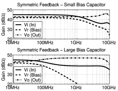
3-8 AC response of symmetric feedback TIA for small/large bias capacitance 3-9 Proposed common-mode feedback (CMFB) TIA biasing ...
3-10 AC response of symmetric versus common-mode feedback TIA . . .
3-11 Extracted AC simulations of two fabricated TIA feedback topologies . 3-12 Test circuit for receiver offset simulation . . . ....
3-13 TIA RF measurement setup ... 69
3-14 TIA eyes at 12.5Gb/s and 18Gb/s for 260fF and 90fF capacitance . . 70
3-15 Jitter as a function of capacitance and input current ... 74
3-16 Receiver jitter versus input signal current and capacitance ... 75
3-17 10Gb/s TIA eyes for varying signal strength, capacitance, and pattern 76 4-1 Pre-emphasis block diagram and basic operation . ... 81
4-2 Simulated rise/fall time improvement with pre-emphasis ... 82
4-3 VCSEL driver output stage schematic . ... 83
4-4 Digital delay line architecture ... 83
4-5 Delay line input data and four output phases . ... 83
4-6 Circuit simulations of pre-emphasis improving the eye diagram . . . . 84
4-7 Die photo of fabricated VCSEL driver . ... 85
4-8 VCSEL driver test setup on RF probe station . ... 86
4-9 Effect of pre-emphasis at 18Gb/s . ... . 88
4-10 Effect of pre-emphasis at 10Gb/s and 18Gb/s . ... 89
5-1 PAM-2 versus PAM-4 at 20Gb/s ... 96
5-2 Probability density and BER for PAM-4 . ... 99
5-3 Symbol values and VCSEL power levels . ... 101
5-4 Architecture of multilevel driver . ... ... 102
5-5 Multilevel VCSEL driver output stage schematic . ... 103
5-6 Layout of PAM-4 VCSEL driver with buffers and output stage . . .. 103
5-7 Circuit simulations of junction current and optical power simulation . 104 5-8 PAM-4 receiver architecture ... 107
5-9 Level shifting pre-amplifier [2] ... ... 108
5-10 2x oversampling front-end latch schematic and timing . ... 109
5-11 Circuit simulation of receiver front end . ... 109
5-12 Transitions with good and bad timing information ... 111
List of Tables
2.1 Estimated and extracted VCSEL parameters used in simulations . . . 43
3.1 Prior work: single-ended transimpedance amplifiers ... 48
3.2 Prior work: differential transimpedance amplifiers . ... 49
4.1 Prior work: high-speed VCSEL drivers . ... . . . 79
4.2 Measured eye improvement data from Figure 4-9 ... 87
4.3 Measured power consumption during PRBS measurement ... 91
4.4 Measured power consumption for DC on/off states ... . . 91
4.5 Equations for calculating block power from data in Table 4.4 .... . 92
4.6 Calculated block power from equations in Table 4.5 ... 92
Chapter 1
Introduction
1.1
Motivation for Optical Interconnect
As processing power scales exponentially with Moore's law, the total aggregate data bandwidth for communication between the components of high-performance computer systems must increase proportionally to prevent a communication bottleneck from limiting system performance. While electrical links have traditionally been employed for interconnects within computer systems, high-frequency loss and interference will eventually limit the performance of these links at high data rates. Optical links have already replaced electrical links for all long-haul data networks and high-performance local networks, and will become advantageous for ever shorter link lengths as data rates increase.
Package-to-package optical interconnects are characterized by many of the same design criteria as long-haul optical links. Ideally, both links are high-speed, low-power, compact, inexpensive, and easy to integrate. However, the relative importance of each of these metrics varies dramatically between the two applications. A long-haul link design may be optimized for speed at the expense of power and cost, but the balance for a package-to-package link is much more complex. The link still requires high speed, but the power consumption, cost, and size must simultaneously be limited to levels that allow the integration of highly parallel optical interconnects. 'Cleaved semiconductor lasers did not provide the performance required to make this type of
Figure 1-1: High bandwidth package-to-package links
link technically and economically feasible, but vertical-cavity, surface-emitting lasers, (VCSELs) [1], have significantly lower threshold current and higher bandwidth and are therefore an attractive solution in this new design space constrained by power, area, and cost.
Figure 1-1 illustrates several package-to-package applications requiring increas-ing bandwidth in future technology generations, includincreas-ing links between processors, bridges, memory, and peripheral IO bridges. While it is clear that higher bandwidth and lower power are required, determining whether electrical or optical links provide better performance for a particular application requires a more complicated analysis based on knowledge of many optical and electrical system parameters. In the past decade, much research has been devoted to predicting when optical links will achieve superior performance as compared to electrical links. While predicting the answer to
this question for future generations requires speculative assumptions about compo-nent performance, a framework for analyzing the effect of each parameter has recently been developed [3]. The work defines the metric of critical length, the link length at which an optical link consumes lower power than an electrical link for a specific set of performance criteria. The model demonstrates that the critical length is reduced for higher bit rates, improved optical devices, reduced optical insertion loss, and lower bit error rates. As scaling to higher bit rates is inevitable, this result indicates that im-provements in optical devices have a direct impact on the performance improvement that can be achieved with optical interconnect. Because there are many variables in the performance analysis, the appropriate metrics for a specific interconnect cannot
be chosen without prioritizing and constraining the system parameters. For example, if a lower bound on bit rate is set a priori, then minimizing the mW/Gb/s subject to the bit rate constraint is appropriate. If an upper bound on power consumption is set instead, then the Gb/s can be maximized subject to this constraint. The relative importance of power consumption and data rate must be determined at the system level in order to arrive at the optimal link design.
Several recent works have made specific predictions regarding the time frame and application space in which optical IO will replace electrical IO. High-performance symmetric multiprocessor (SMP) server systems, in which two or more individual pro-cessors share common memory, require ever increasing data bandwidth in processor-processor and processor-processor-memory links in order to maintain memory and cache co-herency [4]. Recent research suggests that multiprocessor systems and network routers may benefit from intra-card package-to-package optical links as early as 2010 [4]. Even in single-processor systems, processor performance scaling drives an increased demand for bandwidth to memory. In memory applications, some have argued that the dom-inance of memory latency in commodity DRAM in determining memory access time will limit the potential impact of optics for this application [5]. However, while op-tics may have little impact on the physical latency to memory, system level research suggests that that architectural and software techniques applied in high performance systems to mitigate the impact of memory latency will drive increased demand for memory bandwidth [6]. The potential benefits of optical interconnect extend beyond sheer bandwidth performance. Total power consumption promises to become a lim-iting factor in parallel interconnects, and recent work suggests that optical links have a theoretical power advantage over electrical links in the 90nm node at 6Gb/s for critical lengths as short as 43cm [3], and decreasing length for higher data rates. The physical density of interconnect to the chip may also limit the maximum aggregate bandwidth in larger server systems. With the development of dense waveguide pack-ages, optics will have the potential to provide higher linear bandwidth density by eliminating the need for low-loss controlled impedance electrical traces [7].
links have been partially facilitated by decreasing the distance between the transmit-ter and the receiver. For example, one recently published serial link achieved 20Gb/s but could operate at this maximum published rate over only 2 inches of copper [8]. Another electrical architecture with different equalization operates at the full 20Gb/s over 7 inch copper traces [9]. In contrast, optical signals are relatively insensitive to distance and could potentially be used to build flexible IO links to operate over distances between a few inches and a few meters. Such physical flexibility could allow new architectural innovations for high-performance systems.
For both optical and electrical links, maximizing the per-pin data rate is essential because the number of data pins will remain nearly constant across future technol-ogy generations [10]. Instead of channel limitations, optical links must overcome the bandwidth limitations of the optical components in order to achieve maximum per-formance. This requires the application of circuit techniques to compensate for the intrinsic and parasitic bandwidth limitations associated with the VCSEL and photo-diode. CMOS front-end circuitry is the only practical choice for short-distance optical IO as it provides the maximum possible level of integration at the minimum cost.
1.2
Contributions
The three main contributions of this thesis are front-end building blocks designed in 90nm CMOS [11] to maximize the data rates achievable with commercially available optical components. They include a cross-coupled NMOS cascode TIA with 9GHz bandwidth, a digitally tunable pre-emphasis VCSEL driver for 18Gb/s operation, and a PAM-4 VCSEL driver operating at 10GSym/s (20Gb/s).
The feedback TIA is based on a proposed cross-coupled cascode voltage ampli-fier, which increases the gain and bandwidth of a standard cascode amplifier. The technique not only doubles the voltage gain, but also allows gain peaking to optimize the bandwidth by compensating for large load capacitance. A common-mode feed-back biasing technique is introduced to eliminate the low-frequency gain reduction associated with standard symmetric feedback and extend the TIA bandwidth down
to DC. This reduces the link overhead by allowing the transmission of data which is not coded to eliminate low-frequency content. The TIA has a simulated bandwidth of DC to 8.9GHz and measured results demonstrate operation at 12.5Gb/s for 260fF of input capacitance and 18Gb/s for 90fF of input capacitance.
The presented 18Gb/s pre-emphasis VCSEL driver is among the fastest reported CMOS drivers for a commercial GaAs VCSEL. Commercial GaAs VCSELs have sig-nificant capacitance, typically 700fF, and are therefore limited by electrical parasitics as well as intrinsic optical dynamics. In [12], falling edge pre-emphasis reduces the op-tical fall time of experimental 990nm InGaAs VCSELs. These InGaAs devices have smaller capacitance, typically 160fF, and are not significantly limited by electrical parasitics [13]. Dual edge pre-emphasis compensates for both optical and electrical limitations in GaAs VCSELs [14], but the reported architecture has a minimum pre-emphasis pulse width of one bit period and requires phase tuning of the interleaved clocks to minimize systematic jitter. The presented driver derives timing information directly from the full-rate input data and generates pre-emphasis pulses with width resolution less than one bit period in a manner that is compatible with full-rate IO architectures.
A 20Gb/s multilevel (PAM-4) VCSEL driver architecture is proposed as an al-ternative method to achieve higher data rates using standard 10Gb/s class devices. Because short optical links are not typically limited by noise, the optical signal power may be divided into several levels while maintaining an acceptable received bit error rate (BER). When two bits are encoded in each four-level symbol, the symbol rate for an equivalent data rate is reduced by a factor of two, which allows transmission of 20Gb/s PAM-4 data with frequency content comparable to 10Gb/s PAM-2 data. The power consumption of the transmitter is reduced significantly, as this lower symbol rate reduces power consumption in on-chip data paths and eliminates the need for pre-emphasis of the VCSEL current. Extracted circuit simulations and optical rate-equation simulations are presented for the PAM-4 driver. Behavioral simulations of a PAM-4 receiver are presented and receiver complexity is compared for PAM-2 and PAM-4 links.
Chapter 2
Background
Optical links are proposed as an alternative to electrical links, so this chapter begins with a short overview of basic link architectures and the current electrical state-of-the-art in Section 2.1 in order to place this work in context. Since the clock and data recovery (CDR) circuit architectures are similar for optical and electrical links, this overview also provides background for the discussion of PAM-4 CDR architectures in Chapter 5. In Section 2.2, the basic architecture of an optical link and the concept of the link budget are reviewed in order to provide an understanding of how the critical parameters of each component are combined to determine the overall link perfor-mance. Section 2.3 discusses recent research on manufacturable packaging methods for optical package-to-package interconnect. Finally, Section 2.4 describes the meth-ods used to model the optical dynamics of VCSELs. Discussion of prior work on VCSEL drivers and transimpedance amplifiers is reserved for discussion within the respectively relevant chapters.
2.1
Link Architectures: Serial and Parallel
Traditional electrical links are typically divided into two categories: serial links and parallel links. Serial links are generally found in applications where a single channel is used to transmit the data, in which case using an additional channel to transmit a clock alongside the data would introduce unacceptable overhead. Therefore, as
BO
B1
BN
REF
CLK
Figure 2-1: A basic serial link architecture
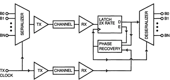
illustrated in the basic serial link architecture of Figure 2-1, the data is transmitted without a forwarded clock and a clock and data recovery (CDR) architecture is used to recover both phase and frequency information from the incoming data and generate an appropriate receiver clock. Perhaps the most common method of clock recovery from random data is sampling the received data twice per bit period, where the data sample (D) nominally occurs in the center of the bit and the edge sample (E) nominally occurs at the transition. A bang-bang phase detector [15] compares each edge sample to the two adjacent data samples in order to decide if the data was sampled early or late. A charge pump then adjusts the VCO control voltage in the direction which moves the clock into alignment with the received optical data.
Serial links with full clock recovery require significant receiver complexity and therefore parallel links, which forward a clock in parallel with several data links, are often used in shorter distance applications when the clock path overhead may be amortized over many data channels. In older technologies, where data symbol periods were long compared to the propagation time in the channel, variations in propagation time were insignificant and the transmit clock could be used directly to retime the receive data. However, as illustrated in the basic parallel link architecture of Figure 2-2, phase adjustment of the data on a per-pin basis is typically required in multigigabit links as channel delay variations are significant with respect to data rate [16], [17]. This requirement has increased the complexity of parallel links and has blurred the previously clear distinction between serial and parallel links. Perhaps modern links are more appropriately categorized by whether the transmitter and receiver share
BO B1 BN TX CL( BO B1 BN
Figure 2-2: One channel of a basic parallel link architecture
a common frequency reference. When no common reference is shared, the receiver must recover frequency and phase information directly from the incoming data. For short links with many channels, expanding the CDR to include this functionality may be more cumbersome than sharing a frequency reference. When a reference is shared, either directly or by a forwarded clock, the receiver must only recover the phase information and the CDR architecture is dramatically simplified.
Two 20Gb/s electrical links in 90nm CMOS demonstrating both embedded-clock and forwarded-clock architectures were presented at ISSCC 2006 [8], [9]. In addition to demonstrating different TX/RX architectures, the works illustrate the increased complexity of electrical links at high data rates, as both employ equalization in or-der to operate at 20Gb/s over only 2-7 inches of copper traces on FR4. In the embedded clock architecture [8], 3-tap equalization with 6b resolution is employed for pre-equalization at the transmitter and a linear equalizer is used at the receiver. Data is serialized and transmitted at 20Gb/s and the receiver uses eight compara-tors, 4x interleaving on both edges of a 5GHz clock, to recover the total of 40GSam-ples/second required for clock and data recovery. These data and edge samples are processed through a bang-bang detector and majority voter to adjust the phase of a local 10GHz LC-VCO. In the forwarded-clock architecture [9], the transmitter uses 4-tap equalization with 6b resolution for transmit pre-emphasis and a continuous-time
BO
B1
BN
REF CLK
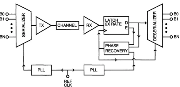
Figure 2-3: One possible hybrid architecture with shared reference clock
source-degenerated equalizer at the receiver. The receiver uses per-pin deskew in the form of an eight-stage DLL and phase interpolator to generate a four-phase clock to drive the 4x interleaved sampling comparators.
The simultaneous publication of both forwarded-clock and embedded-clock sys-tems indicates that the choice between these two architectures is not yet obvious for short-distance links. Unlike long-haul links, where the overhead of sharing a frequency reference is clearly prohibitive, in shorter links with many data pins this overhead may be less onerous than the additional complexity of recovering both frequency and phase at each pin. Furthermore, in an architecture with TX/RX parallel links transmitting in both directions, use of a shared reference frequency could further simplify the ar-chitecture. Assuming PLLs are used at both ends of the link to generate low-jitter and high-frequency transmit clocks, simply locking both PLLs to a shared reference would guarantee identical frequency of the local clocks at both ends of the link. Then, local per-pin phase recovery could be used to align each receive clock to the incoming data as illustrated in Figure 2-3.
While clock and data recovery is not the focus of this thesis, behavioral modeling of a PAM-4 receiver to demonstrate the benefits of using edge selection to eliminate PAM-4 edges with bad timing information is a significant component of Chapter 5 and certain assumptions must be made about the CDR architecture in order to implement
such a system. The PAM-4 receiver architecture will assume that a full-rate clock is available, either from a directly forwarded clock or from a shared reference clock architecture such as the one illustrated in Figure 2-3. Timing recovery at the receiver is then implemented with a DLL and digital phase selection and interpolation, which may now occur at a lower loop bandwidth to minimize the jitter contributed by the bang-bang phase detector. Because DLLs are more stable than PLLs and can tolerate more latency in the feedback loop, this architecture also allows for CDR logic to be performed after deserialization in order to reduce power consumption. This will be particularly advantageous for PAM-4 clock recovery which requires more complex logic and is discussed in more detail in Chapter 5.
2.2
Optical Links: Components and Link Budget
At the most basic level, an optical link consists of a transmitter, channel, and receiver. The transmitter converts electrical data to a modulated optical signal, which then propagates through the channel and is converted back into the electrical domain at the receiver. Design constraints for links with different target applications place significantly different requirements on these three sub-systems. The design space for short-reach optical links prioritizes high data rate, low power, low cost, and compact form factor. This encourages the use of low-cost, highly integrated CMOS transmitter and receiver circuits and low-threshold current VCSEL devices. While longer links can compromise on cost, power, and form factor to achieve higher data rate, package-to-package links will not be practical without meeting challenging targets for each of these specifications. However, due to shorter link length and channel loss, transmit power and receiver sensitivity requirements are relaxed.
The link budget provides a mechanism for analyzing the system performance im-plications of each component. The signal and noise power at each stage in the trans-mission process are analyzed in order to guarantee that the signal power incident to the receiver allows acceptable system performance. A basic analysis of link budget-ing is presented here for the specific case of a short optical link and further details
Ught Output
Electrode r...
Figure 2-4: The VCSEL device structure of [1]
and theory may be found in most introductory texts on optical communications [18]. First, the power budget considerations for the transmitter, channel, and receiver are discussed and representative values are determined. Finally, an example link budget analysis using the determined values is presented.
2.2.1
VCSEL and Transmit Power
The vertical-cavity, surface-emitting laser (VCSEL) is a small laser device fabricated in the plane of the substrate. A light-emitting diode structure with a quantum well gain medium is fabricated inside an optical cavity consisting of two distributed Bragg reflectors (DBRs). The basic structure of a modern VCSEL is shown in Figure 2-4, which is reproduced from an invited paper presented in 2000 by the inventor of the VCSEL, K. Iga [1]. The VCSEL is ideal for short optical interconnects due to its small size, low threshold current, and suitability for array integration.
When a VCSEL is biased above threshold, the output power of the device is ap-proximately a linear function of the junction current. The current through the device is modulated between two current levels ('0' and '1') to transmit a binary signal. The
small-signal bandwidth of a VCSEL increases with the current and the lower bound on the '0' current is therefore determined by the minimum bias over threshold that re-sults in sufficient bandwidth. The upper bound on the '1' current is imposed by power consumption, reduced laser efficiency due to device heating, and reliability concerns. Most commercially available high-speed 850nm VCSELs have a threshold current of ImA to 2mA, a usable current range of about 2mA to 10mA, and a slope efficiency of between 0.3mW/mA and 0.5mW/mA [19, 20, 21]. In a typical transmitter design, the VCSEL might be modulated from 2mA to 8mA. If we assume a device with a threshold of ImA and slope efficiency of 0.4mW/mA, this results in a '0' power of 0.4mW and a '1' power of 2.8mW. The average power is then 1.6mW (2.0dBm) and the optical modulation amplitude (OMA) is then 2.4mW (3.8dBm). This calculation is an example of the maximum power that can be transmitted with existing high-speed GaAs VCSELs. If lower power is required by the system constraints, the '1' current may be reduced accordingly. However, if high-speed performance is of utmost importance and power consumption is secondary, the VCSEL might be biased with a larger average current and smaller OMA. In further discussions throughout this thesis, references to the transmitted optical power of the VCSEL refer to the mod-ulation power or OMA, since this quantity is most significant for analyzing receiver performance. While only the modulation power aspect of VCSEL performance is considered here, further details on the high-speed performance and optical dynamics are found in Section 2.4. Once generated, this modulated optical signal is launched into the optical channel.
2.2.2
Optical Channel
Unlike the copper traces used for high-speed electrical interconnect, optical channels exhibit negligible frequency-dependent losses. From this perspective, the primary challenge for obtaining high-speed operation of an optical link lies in the electrical-optical and electrical-optical-electrical conversion. However, electrical-optical packages for short links play a critical role in providing a high quality optical channel and thereby maxi-mizing system performance. For example, although coupling loss in the channel is
independent of frequency, it has a direct and often significant impact on the link bud-get through the relationship PTx-PLoss=PRx. A channel with significant coupling loss will impact the system by requiring increased transmit power or receiver sensi-tivity, both of which come at the expense of power consumption, area, and circuit complexity. Therefore, loss reduction as a result of ongoing research on optical in-tegration [22],[23] will relax the design constraints on remaining system components and improve overall link performance. For this work, the worst case expected channel loss through the optical package is 12dB [22].
2.2.3
Receiver Sensitivity
Optical receivers typically consist of a photodiode and transimpedance amplifier and their important performance metrics are bandwidth and sensitivity. Receiver sensi-tivity is defined as the minimum received power that allows the receiver to resolve the signal with a specified bit error rate (BER) and is therefore a function of the total noise at the receiver due to both the photodiode and receiver circuits. Analysis of receiver sensitivity is generally quite complex, but may be simplified in most P-I-N diode receivers since the dominant causes of receiver degradation are limited to shot noise in the diode and input-referred noise from the receiver circuits. The interested reader may refer to [24], [25], [26], and [27] for a more detailed analysis.
In beginning an analysis of receiver sensitivity, it is helpful to first quantify the total equivalent input current noise, I~e, since input current noise may be directly related to the signal photocurrent to determine the signal-to-noise ratio and therefore the sensitivity for a given BER [18]. It is important to note that I eq does not describe
a real physical quantity, but is simply defined as the square of the total output voltage noise divided by the peak magnitude squared of the receiver transfer function, R2 ,
as in (2.1). The definition and calculation of Ieq effectively refers the total output noise to the peak magnitude frequency of the receiver transfer function and allows direct comparison of this quantity to the received signal current if we assume that the signal power occurs within the band where IZt(f)l Rt. (Here, the receiver
transfer function, Rt is the peak magnitude, and Ht(f) is the amplitude-normalized,
frequency-dependent component.)
V2
I2 - no (2.1)
To find Ieq, V,2 is first determined by integrating the output noise spectral density,
2 put-referred
vo, over all frequencies as in (2.2). Next, (2.3) relates vo to the input-referred noise spectral density, i2 e through the transfer function, Zt(f). Finally, the Rt term is
separated from the transfer function to reach a solution for Ie (2.4). Several methods exist for analytical calculation of the integrals when simplifying assumptions are made about the amplifier transfer function [28], [18], [27]. In this work, when considering the TIA design of Chapter 3, we will use simulation to determine the input-referred noise spectral density and then assume a noise equivalent bandwidth (NEB) to approximate the total equivalent input noise current.
V=o
o (f)df (2.2)v
=i
2(f)zt(f)
2df(2.3)
[I2 = i2 , (f)l ,(f)l2df (2.4)
Once the total output voltage noise and total equivalent input current noise are calculated and a maximum allowable BER is specified, it is possible to calculate the minimum allowable received power. This sensitivity analysis is relatively simple for the particular case of optical receivers based on P-I-N diodes, as it has been previously shown that the noise is dominated by electronic receiver noise and that representing the noise as a signal-independent Gaussian distribution typically yields results accurate to within 1 dB [28]. Furthermore, because high-speed operation of VCSEL transceivers requires a relatively significant bias above threshold, the analysis
keeps the general case of a non-zero received power for the '0' bit but assumes that dark current in the diode is negligible.
To derive the probability of error, following the analysis of [18], we begin with the assumption that the probability density function of the output voltage noise of the transimpedance receiver is described by (2.5) and (2.6), where Vo is taken from the result of (2.3) and vo and vl are the nominal expected values of the output for either
a received '1' or 'O'.
Po(v) = exp -2V)2 (2.5)
V2_ r V%
2
Vn2
1 (v1 - v )2
P(v)
=
exp
(-)2V
(2.6)
If we define the voltage threshold of the decision circuit following the TIA to be
vt and assume that '1' and '0' are received with equal probability, then the total
probability of error is the average of the integral of Po(v) for v > vt and the integral of Pl(v) for v < vt as shown in (2.7). It is clear that the choice of threshold is critical and it can be shown that the optimal threshold is exactly centered between the two expected values if the noise present in the system is signal-independent and the symbols occur with equal probability.
1jOj[
1
p(v
-
vo)2)]PE
2
vy,
f
exp
e
eV,,
2Vn2
(2.7)
+1
vt
exp1( v - Vl)2)]These functions are not analytically integrable, so the function Q(z) is defined to simplify analysis (2.8).
Q(z)-
exp-
dx(2.8)
S%-27
z
(- 2
By completing separate substitution of variables on (2.7), x=(v - vo)/V,, for the first term and x=(v1 - v)/V,, for the second term, (2.7) is expressed in terms of the
Q function as in (2.9). Applying the further assumption that vt is optimally centered
at the average of vo and vl, then v, - vt = vt - _o 2=V' and this expression is
further simplified to (2.10).
PE (V - t) 1 ( - vo) (2.9)
PE = - Q V9) (- 9Q
2
Vn 02
VnoPE = Q ( •- : (2.10)
The function describes the total probability of error and may be referred back to the receiver input and parameterized with respect to the input power and the total equivalent input noise current fIne (2.11), where R is the receiver sensitivity and Po
and Pi are the power levels received for '1' and '0'.
pE = ( R" (PI - Po) )
PE =
Q
(R PO)) (2.11)The required value of PE is specified at the system level by the BER. In order to determine the minimum received modulated power, P1 - Po, a table of numerically
computed values of Q(z) may be used to determine the required value of the
Q-function argument, QF, for the specified BER. Figure 2-5 plots this calculation and illustrates the required QF values for common BER specifications. It is useful to
remember that we require approximately QF= 6 for a BER of 10-9, QF=7 for a BER of 10-12, and QF=8 for a BER of 10-15. Once the BER is chosen and the
Calculation of Q for Common BER Specs LU w o 0 0 -j Q-Function Argument
Figure 2-5: Q-function calculation for BER=[10-9, 10-12, 10-15]
calculated as in (2.12) and the associated receiver sensitivity is calculated as in (2.13).
2
- Po =eqR
Sensitivity = 10 log
(
P - Po)1
mW
(2.12)
(2.13)
Details on the analysis of Ieq and determination of the sensitivity for the designed receiver are provided in Chapter 3. The worst case result is -10dBm at a BER of 10-12, which is comparable to other reported CMOS receivers designed for 10Gb/s operation.
2.2.4
Example Link Budget Analysis
The link margin is defined as the difference between the received power and the receiver sensitivity, and must be positive to ensure that the link meets the target specifications. For the example case, assume that the VCSEL transmits OdBm optical
power. Subtracting a typical link loss of 8dB leaves a received power of -8dBm, which is 2dB greater than the worst-case expected receiver sensitivity of -10dBm and will therefore result in correct link operation. In practice, many additional factors and noise sources may be included in the link budget analysis. Details may be found in [18], but this basic example provides a starting point for a simple link budget analysis.
2.3
Integration and Packaging Methods
Demonstration of compact, cost-effective, manufacturable packaging and integration techniques is necessary in order for optical package-to-package interconnects to be-come a practical alternative to electrical links in short-reach systems. As a result, a significant amount of recent industry research has focused on the implementation of such techniques. Many variations with different advantages and challenges have been proposed and are summarized in this section.
2.3.1
Single Wavelength
Parallel single-wavelength links were the first proposed alternative and remain the best candidates for practical integration in the near term. Alternate package architectures have been proposed by Intel in [22] and [23] and by the Terabus project in [29]. The two packages are illustrated for comparison in Figure 2-6.
The Intel package of Figure 2-6(a) provides dual 1x12 optical channels to the same CMOS chip to allow simultaneous transmit and receive. This is accomplished by flip-chip bonding the CMOS chip and the 1 x 12 optical component arrays to a small organic substrate and making an electrical connection between them with short copper traces. This approach is attractive as the manufacturing techniques are more mature than those proposed by the Terabus project and because the the thermal coupling between the CMOS and optical components is dramatically reduced, which will improve VCSEL performance and reliability. However, the traces connecting the CMOS and optical components are several millimeters long and must therefore be treated as transmission lines at higher data rates. For example, the 10GHz
funda-- funda-- funda-- funda-- funda-- funda-- funda-- Optical Connector ---I - - - - - Optical Waveguide ---SI r - 50 Ohm TXLine- I
VCSEL I CMOS Chip , PD
Output Input
Optical Optical
Connector Package Substrate and Electrical I0 Connector
Board
(a) Intel Optical Package
Silicon carrier with
wiring and vias
TX CMOS RXCMOS
V"XL -PD
' Polymer Waveguide ' 1
Gold
,r
Card with surface wiring(b) Terabus Optical Package
Figure 2-6: Two proposed packages for high-density optical interconnect mental of 20Gb/s data has a wavelength of 1.4cm assuming a substrate with a relative permittivity of 4.4. These short traces are near the boundary where traces must be treated as transmission lines, which occurs when their length exceeds one-tenth of the shortest wavelength [30], which in this case occurs at 1.4mm. A terminated driver was therefore designed for use with this package architecture.
The Terabus package of Figure 2-6(b) provides a 4x 12 single-direction optical channel from a CMOS transmitter chip to a CMOS receiver chip. The front of the CMOS chip is first bonded to a silicon carrier with through-silicon vias and surface wiring to provide power and electrical signals to the transmitter or receiver. A 4 x 12 VCSEL or photodiode array is then flip-chip bonded to the sub-assembly consisting of the CMOS chip and silicon carrier -the optical devices are bonded front-to-front with the CMOS chips but etched lenses allow optical coupling through the back side. This entire assembly is bonded to an optical card and waveguide, so the optical signals are then turned at a right angle with gold plated mirrors into a polymer waveguide mounted on the board. While the package does not integrate transmit and receive functionality onto a single chip, it provides higher aggregate data capacity for a one-way link, and future dual-direction link implementation is not precluded. The integration process, which is more complex than that of the Intel package, allows direct integration of the VCSEL and photodiode onto the CMOS chip. This allows the use of high-impedance VCSEL drivers, which provide power savings as compared with terminated drivers. However, VCSEL reliability and performance issues resulting from the close thermal coupling of the VCSEL and CMOS in this design require careful thermal management.
Figure 2-7: Multiple wavelength MAUI package
2.3.2
Multiple Wavelength
In addition to the described single-wavelength links, multi-wavelength coarse wavelength-division multiplexing (CWDM) has been proposed to increase the total aggregated data rate for an interconnect limited system [31]. This proposed package, which provides a one-direction 1 x 12 x 4A optical channel, is illustrated in Figure 2-7. The CMOS chip is used as a base for the assembly and includes a 4x 12 array of sites for flip-chip bonding optical components and an additional set of pads around the perimeter for wire bonding the CMOS to the package substrate. Four 1 x 12 arrays of optical components are flip-chip bonded front-to-front with each CMOS chip to provide the four wavelengths of 990nm, 1020nm, 1050nm, and 1080nm. The devices are bottom-emitting and the optical signals are therefore coupled out through lenses etched in the back surface of the optical components. A silicon seal ring is bonded to the CMOS to provide a hermetic seal and set the spacing between the CMOS base and the optical MUX/DEMUX. Optical MUX/DEMUX devices are then bonded to the seal ring. These components allow the transmission of 48 optical signals through 12 fibers by combining one signal of each wavelength into each physical channel. Finally, an alignment structure is bonded to the top of the stack to allow physical alignment with standard optical MT connectors. Development of manufacturable integration methods for wavelength division multiplexing will facilitate higher data density, but as optical multiplexing occurs after the electrical to optical conversion, it will not influence the design of the interface circuits unless different methods for the CMOS interface to the optical components are required.
2.4
Modeling Methodologies
While accurate compact models for transistors already exist and photodiodes may be simply modeled as capacitors, VCSEL modeling for circuit design applications is a relatively new area of research and selection/implementation of an appropriate model is an important part of any driver design endeavor. This section discusses model requirements and reviews prior work. The selected model is fit to data published in the literature for a commercial GaAs VCSEL [21]. This device was selected since the paper presented the most complete set of electrical and optical data for fitting the model.
2.4.1
Model Requirements and Prior Work
VCSELs may be simulated at many levels of detail. Full finite-element simulations may be required to model the most complex effects, but these types of simulations are computationally intensive and incompatible with standard circuit simulation environ-ments. However, simple rate equations with no consideration of spatial dependence do not model effects such as carrier diffusion and spatial hole burning and may be inappropriate for simulations requiring high levels of accuracy.
In order to select an appropriate level of model complexity, it is necessary to consider both the availability of suitable characterization data and the intended use of the model. Since the model parameters must be fit to the actual VCSEL device, the model complexity should not exceed the available level of device characterization data. For the case of the VCSEL driver design, it is important for the VCSEL model to capture the AC and DC characteristics of the VCSEL output power and the electrical parasitics of the VCSEL. Furthermore, given the limited interaction between VCSEL suppliers and circuit designers, the model should contain only parameters that may be approximated from the literature or fit to the VCSEL using relatively simple measurements such as S-parameter data. Model accuracy near threshold is not essential because bandwidth limits at lower bias currents prevent high-speed drivers from operating VCSELs in this range. Given these constraints, models based on rate
equations are the most appropriate choice.
Much of the relatively recent work on rate equation models has investigated meth-ods of transforming the spatiotemporal rate equations into systems of ordinary dif-ferential equations [32], [33], [34], [35], [36], [37]. This approach assumes an arbitrary number of optical mode profiles a priori, represents the electrical carrier density as a finite set of terms in a Bessel series expansion, and leaves weighting coefficients for the carrier densities in each optical mode and series expansion term as the only un-knowns during simulation. This method is flexible and may be used to retain either radial or radial and azimuthal dependence and for an arbitrary number of optical modes. However, the fitting of these models requires knowledge of the mode profiles of the VCSEL and since this kind of data is rarely reported in literature or data sheets, a spatially-independent rate equation model is much more practical. Recent work [38] has demonstrated that such models may be used in conjunction with simpli-fied linear electrical VCSEL models to provide sufficient accuracy for opto-electronic co-simulation of VCSEL drivers using 10Gb/s GaAs VCSELs.
2.4.2
Electrical Model
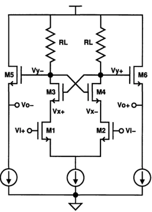
An electrical VCSEL model must be developed in order to simulate the electrical interaction of the VCSEL with the driver circuits. A diode junction model and ap-propriate parasitic capacitances and resistances may be used in conjunction with the intrinsic rate equation model to provide a complete description of the laser. How-ever, this requires co-simulation of Verilog-A and may result in convergence issues in some simulators. If the VCSEL will only be operated above threshold, the diode model is nearly linear and may be modeled as a resistor and voltage source in series for ease of simulation. Parasitics associated with the package, the bond pad, and the DBR are reported to be constant across bias and may therefore be included as linear elements from the standard circuit simulator. The complete electrical model is shown in Figure 2-8, where Rp=90Q, Cp=50fF, RDBR=19Q, Cj=700fF, and a 1.5V source and 45Q resistor were substituted in series for the intrinsic diode [21]. The current flowing through the VCSEL junction was exported from Cadence and optical
IJCT
Figure 2-8: Electrical parasitic model of VCSEL
simulations were completed in Matlab.
2.4.3
Optical Model
The following analysis of optical rate equation dynamics, expanded from a recent paper on rate equation modeling of VCSEL devices [38], is described in sufficient detail to allow its implementation and use by other circuit designers. The equations of (2.14) and (2.15) describe the interaction of photons and electrons when the effect of the separate confinement heterostructure (SCH) is neglected. The carrier densities experience relaxation oscillations in response to sudden changes in the injected current which result in overshoot of the VCSEL output power. Attempts to fit this model to the measured VCSEL data yielded small-signal AC results with excess gain peaking which would cause any transient simulations to predict pessimistic levels of overshoot. This suggests that an addition real source of damping may be neglected by this model.
dPt [1] 1 P ]govg + N + 1 + CP (2.14)
d- = -
I
I-
I
N-g
-
Nt
P
(2.15)
dt qV TN 1 + 6P
Adding a third equation to model the interaction between the electrons in the quantum wells and the electrons in the SCH yields a better-matched result since
this effect increases the damping of the photon-electron interaction and reduces over-shoot. The variables P, N, and M represent, respectively, the photons, electrons in the quantum well, and electrons in the SCH.
dt -
[I
P
+
N
+
govg
P
(2.16)
d t
T
TN
1 + eP
dN _1
r1
1
[ lN
- N
"- = 1 M- - [N + _1 N - gov, [ P (2.17)dt
rq~cap
TN
Tesc
1 + EP
dt-
[q
]
I -[
M +
[
N
(2.18)
dt
qV
Tcap
Teac
By setting the time derivatives equal to zero and solving the equations of
(2.16)-(2.18) the DC solution given in (2.19)-(2.24) is obtained. (The results for No and Po
are also valid for the solution of the rate equations of (2.14)-(2.15).)
-b + Vb-2 - aC
Po = 2 a o (2.19)
2a
No T-1
(-
S•
+ (2.20)(1 - o) \F-rr qV/
Mo = Teap [r-sio +
E±
No, (2.21)TngOvg + E
a
=
rngovg +-
(2.22) 1pg(1 - 3)b =govgNtr
+ nrg (1- ) np I- [7 n--/) Io (2.23) o) qV (1-fl) c = - [q(1-fl) (2.24)The AC solution to the rate equations may be found by expanding the non-linear term using the linearization term given in (2.25).
N-Ntr p~4NP
[
o P(No - Ntr)-Nt
p + P+
EP (1-)
(2.25)1+ 1P1 + E Po (1 + EPo)2
The linearized versions of the rate equations giving the AC solution (P,N,M) around any given DC operating point (Po,No,Mo) are given in (2.26)-(2.28).
dP p N NPo P(No - Ntr) (2.26)
dt P 1 + ePo (1 + EPo)2
dN
d-
= -[1
]
M-1
Te1NPo
P(No
-
Ntr)
(2.27)
+ -·
gov
+ (2.27)dt F ap -N Tesc 1+ EPo (1 + ePo)2
dM
t
=
qv
e
I-
1
M +
[ ]
N
(2.28)
dt iqV LTcap LTesc
(2.28)
After taking the Laplace transform, (2.28) may be solved for M as a function of I and N as in (2.29). This result is then substituted into the Laplace transform of (2.27) and the similar terms collected to give (2.30) and the terms of the Laplace transform
of (2.26) are collected to give (2.31), with the constants (2.32)-(2.35) defined for
readability.
M Tcaprq i I + -N (2.29)
(1 + s•-ap)
[qV
TescNscsc
Tesc(1 + Scap) =[q(1
+scap)
(2.30)73 F govgPo kl = + 7n 1 + EPo
1
r90ov
(No
-
Ntr)
k = p2 7P (1 + eP)2 1 gov9gP k3 = - + r7 1 + EPO k - govg (No - Ntr) (1 + ePo)2(2.32)
(2.33)
(2.34)(2.35)
Finally, (2.30) and (2.31) are combined to the result of (2.36) which gives the AC solution for the photon density as a function of only the AC input current.1 e 1 )
Tesc Tesc(1 + STcap)) + kik4
- ik I
Note that if at this point we let T
cap = 0 and ,,es =
oc
then this result simplifiesto the AC solution of the rate equations with no SCH. In that case we would find the modulation transfer function (MTF) of (2.37).
P
82S2
+
yS + W2
A
P=
qV 7 = k2 + k3 w = k2k3+ klk 4 (2.37) (2.38)(2.39)
(2.40) If, instead, we keep the extra terms we can use the definition of (2.41) to simplify the solution and the MTF of (2.37) is modified to include the sub-terms of (2.42)-(2.44).VCSEL Response: Data and Model
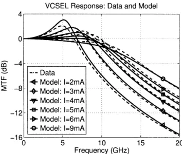
Figure 2-9: AC comparison of measurements and model
= + 1 + ScapTcap /Tesc
(qV)(1 + Scap)(X) X 2 k2ka + klk4 Wo =
X
(2.41) (2.42)(2.43)
(2.44)2.4.4
Model Fitting
The existence of analytical DC and AC solutions allow efficient model fitting. A detailed analysis of the sensitivity of the VCSEL parameters is presented in [38],
which concludes that a majority of the VCSEL parameters may be set based on their design values or taken from the literature but that the performance is strongly dependent on the accuracy of a select set of parameters which must therefore be
![Figure 2-4: The VCSEL device structure of [1]](https://thumb-eu.123doks.com/thumbv2/123doknet/14344679.499807/26.918.258.671.131.473/figure-vcsel-device-structure.webp)
![Figure 2-5: Q-function calculation for BER=[10- 9 , 10-12, 10-15]](https://thumb-eu.123doks.com/thumbv2/123doknet/14344679.499807/32.918.261.677.127.480/figure-q-function-calculation-ber.webp)