HAL Id: hal-00672244
https://hal.archives-ouvertes.fr/hal-00672244
Submitted on 20 Feb 2012
HAL is a multi-disciplinary open access
archive for the deposit and dissemination of
sci-entific research documents, whether they are
pub-lished or not. The documents may come from
teaching and research institutions in France or
abroad, or from public or private research centers.
L’archive ouverte pluridisciplinaire HAL, est
destinée au dépôt et à la diffusion de documents
scientifiques de niveau recherche, publiés ou non,
émanant des établissements d’enseignement et de
recherche français ou étrangers, des laboratoires
publics ou privés.
Low-Temperature Copper Bonding
Bassem Mouawad, Maher Soueidan, D. Fabregue, Cyril Buttay, Bruno Allard,
Vincent Bley, Hervé Morel, Christian Martin
To cite this version:
Bassem Mouawad, Maher Soueidan, D. Fabregue, Cyril Buttay, Bruno Allard, et al.. Application of
the Spark Plasma Sintering Technique to Low-Temperature Copper Bonding. IEEE Transactions on
Components and Packaging Technologies, Institute of Electrical and Electronics Engineers, 2012, 2
(4), pp.553 - 560. �10.1109/TCPMT.2012.2186453�. �hal-00672244�
Abstract—Planar structures, in which a power die is soldered on a substrate and wirebonds are used to connect the top of the die with the substrate, are limited in terms of thermal management and power density. Three-dimensional packaging techniques have been proposed to overcome these limits. Here, an innovative copper-to-copper bonding solution is presented, that can be used for 3-D packaging. The bonding process is described and the effect of the bonding parameters is investigated. It is found that this technique is compatible with the requirements of power electronic packaging. A test assembly including a silicon power die and ceramic substrates is presented.
Index Terms—semiconductor device packaging, power elec-tronics, Spark Plasma Sintering, Three-dimensional packaging.
I. INTRODUCTION
P
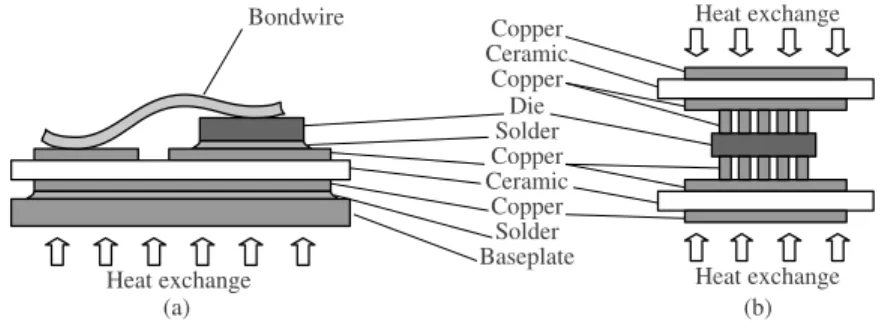
OWER SEMICONDUCTOR DEVICES have largely im-proved since they were first introduced more than 50 years ago. The recent availability of silicon carbide (SiC) devices as a replacement of the classical silicon-based components has pushed the boundaries even further in terms of power density, conversion efficiency, switching speed or thermal capability.Classically, several power dies are assembled into modules such as described in figure 1(a). Such a package provides the electrical interconnects (via the wirebonds and the copper tracks of the ceramic substrate), the electrical insulation (using the ceramic substrate), and the thermal management (the heat dissipated by the devices is removed through the ceramic layer . This structure is used in the vast majority of the power modules that are currently manufactured.
However, this planar packaging solution has become the limiting factor of the performances of the semiconductor modules. The use of wirebonds, which have a stray inductance that can exceed 10 nH [1], increases the switching losses of the devices and limits the plain usage of the semiconductor area as well as the switching frequency. From a thermal point of view, with a classical “planar” package, all the power dissipated by a device is evacuated through its bottom side only. A cooling
January 16, 2012
Mr Mouawad, Soueidan, Buttay, Allard and Morel are with the Universit´e de Lyon, F-69621 France, CNRS UMR 5005, INSA Lyon, Laboratoire Amp`ere, bˆat. L. de Vinci, 21, avenue Capelle, F-69621, Villeurbanne. Mr Fabr`egue is with the Universit´e de Lyon, INSA de Lyon, MATEIS-UMR 5510, Bˆat. Saint-Exup´ery, 25 avenue J. Capelle, F-69621 Villeurbanne Cedex, France. Mr Bley is with the Universit´e de Toulouse, LAPLACE, Universit´e Paul Sabatier, CNRS, UMR5213, Toulouse, F-31062, France. Mr Martin is with the Universit´e de Lyon, F-69622 France, CNRS UMR 5005, Universit´e Claude Bernard Lyon 1, Laboratoire Amp`ere, bˆat. Omega, 43, boulevard du 11 novembre, F-69622, Villeurbanne.
system that could remove the heat through both sides of the die would be much more efficient.
Replacing the planar structure and its wirebond intercon-nects is not an easy task, as it is a very mature solution. Many research groups are working on alternative architectures, some focusing on replacing the wirebonds by a flex substrate [2], or with a screen-printed paste [3]. Other researchers have worked on so-called “sandwich structures”, which use two similar substrates with the dies in-between. These solutions are designed to offer double-side cooling of the devices [4], [5]. Several papers have been dedicated to the comparison of the various 3-D structures [6]–[8].
II. PRESENTATION OF THE3-DSTRUCTURE
A. Description
As mentioned in the previous section, a three-dimensional (as opposed to planar) structure is needed to take full ad-vantage of the power devices. A possible solution for such a package is depicted in figure 1(b) [9]. The originality of the presented technique is that copper posts (or pillars) are grown electrochemically on the die. These posts are then bonded to a Direct Bonded Copper (DBC) substrates on both sides. DBC is basically a ceramic tile with two layers of copper, one of them being patterned to form an electrical circuit.
Such a structure offers double-side cooling capability. Fur-thermore, using copper posts instead of a single, massive interconnect should give more freedom for the system to accommodate the thermal expansion of copper (which is 17 ppm/K, as compared to less than 4 for Si or SiC). One of the advantages of this technique is that we can set the height of the posts to insure sufficient spacing between the DBC tiles and the die. This is required to sustain the required voltage (1200 V or more).
Another advantage of the post structure is that it can accept dies of different thicknesses in the same package, by varying the height of the posts.
However, this “micro-posts” structure has a drawback: the effective interconnect area is smaller than in the case of a single, massive post. With the current design, the copper posts only represent 25 % of the die contact area (the remaining 75 % is the space around the posts). From an electrical point of view, this area is sufficient as it is already more than what is attainable using wirebonds. From a thermal point of view, however, a special care must be given to achieve a low thermal resistance. In particular, only materials with a very high thermal conductivity should be used for the interconnections,
Fig. 1. A planar module (a) and the proposed ”3D” structure based on micro-posts, which offers double-side cooling
including the bonding between the posts and the DBCs. There is an interest to remove the inner bonding material. For this reason, it was decided to develop a special direct copper-to-copper bonding technique.
B. Fabrication
The first step to achieve a structure such as described in figure 1(b) is to grow copper posts on the semiconductor die. This is described in details in [9]. Thin Ti and Cu layers (20/100 nm respectively) are deposited on the aluminium pad of a die (to make it compatible with the following precess steps). Then, a thick photoresist layer (in our case a 75 µm-thick Riston PM275 dry film) is applied on the die and patterned. Finally, the copper posts are electrochemically grown through the openings of the photoresist film, polished to obtain a flat surface, and the photoresist is removed.
In the technique described in [9], a layer of tin (0.5 µm) is deposited on top of the posts. This layer is used as a solder between the posts and the copper of the DBC substrate. The die-to-DBC assembly is performed in vacuum, under a pressure of 10 MPa and at a temperature of 200 °C. This results in the diffusion of the tin layer in the copper parts.
Another assembly approach, described in this paper, is to get rid of the tin layer, and to achieve a direct copper-to-copper bonding (that is, to bond the micro-posts to the DBC substrate without any additional material). This technique is promising, as it reduces the number of processing steps. Furthermore, a good thermal performance can be expected, as only copper is used.
C. Review of the low-temperature direct bonding techniques for Copper
Packaging techniques used to bond conductive parts usually rely on soldering. Many soldering alloys exist, with various properties (such as their melting temperature), but they all offer medium to low thermal conductivity (less than 50 W/K.m) [10]. The melting temperature of the solder alloys, which is usually between 200 °C and 350 °C also sets a limit to the operating temperature of the whole power module [11]. Furthermore, a power module comprises many layers (figure 1). Such a stack of materials with different CTEs is prone to failure when submitted to temperature cycling.
Therefore, we have tried to get rid of the not-so-conductive layers, as well as to reduce the materials count by bonding
directly the copper posts onto the copper metallizations of the substrate. Such a solution is also expected to operate satisfac-torily at elevated temperatures, as the melting point of copper (1084 °C) is much higher than that of the classical solder alloys. Copper has attracted much attention in the area of very large scale integration (VLSI) interconnection technology as the most prospective candidate for the conducting material due to its high electrical conductivity and high electromigration resistance compared with aluminium [12], [13]. It is also a material compatible with industrial processes.
Several experiments on Cu/Cu direct bonding have been reported [14]–[16]. Although the presented methods are sim-ple, they require either high external pressure and annealing or toxic chemical cleaning processes to achieve a reasonable bonding strength. For example, Cu wafers exhibit good bond-ing properties when Cu/Cu contacts are carried out at 400 °C and 4 bar for 30 min, followed by an annealing cure at 400 °C for 30 min in N2 atmosphere [17].
Another solution, the so-called Surface Activated Bonding “SAB” process was used to bond Cu-coated wafers at room temperature without any wet chemical process. SAB is a process that joins similar or dissimilar materials by means of the adhesion force between atoms of two atomically clean sur-faces under an ultrahigh vacuum (UHV) at room temperature [18], [19]. The same authors also reported that the bonding strength of Cu/Cu interface is approximately 6.47 MPa [20]. J. W. Elmer et al. [21] have presented a diffusion bonding of high purity copper using a conventional furnace. A series of diffusion bonds was performed to determine the relationship between bond strength and bonding parameters in order to determine a range of bonding conditions. These tests were made over a wide range of temperature (from 400 °C to 1000 °C), with different bonding pressures and surface states. In these studies, the bonding time was held constant (60 min) at the peak temperature, following a 30 min warming ramp. Bonding strengths of 65 MPa and 190 MPa were found using uniaxial tensile test for samples bonded at 400 °C and 800 °C respectively.
In general, a high temperature annealing cure (>400 °C) is required to increase the bonding strength. However, semi-conductor devices have been designed to meet the requirement of the existing soldering technology (a few seconds above 300 °C). Therefore, an increase in the process temperature could require heavy modification in the dies manufacturing parameters to avoid possible degradation. This is especially
Fig. 2. Temperature profile during the bonding process. Pressure (16 to 76 MPa) and vacuum (10−2Torr) are applied during the entire cycle.
true for longer bonding process such as those involving chemical species diffusion, as they last from minutes to hours. In addition, a low temperature process is advantageous in terms of manufacturing costs. Finally, keeping the process temperature to a low level reduces the residual mechanical stresses of the assembly. Therefore, lowering the temperature for Cu/Cu direct bonding is a key issue in various future device applications. An alternative solution, which uses an electroless deposit of copper to fill the gap between two copper posts, and thus create a low-temperature bond, is presented in [22]. This technique offers a very good bonding strength (>148 MPa).
The solution presented in this paper is based on a different approach, as no chemical solution is involved during the assembly. To the best of our knowledge, Cu/Cu direct bonding using Spark Plasma Sintering (SPS) has never been reported. In this paper, we focus on the bonding issue by evaluating the bonding strength as a function of temperature, pressure and bonding time.
III. BONDING OFCOPPER
A. Sample Preparation
Commercial copper rods (Goodfellow, Cambridge, UK, 99.99+% purity) with a diameter of 19 mm and a length of 400mm were used as the base material in the bonding experiment. These rods were cut into 25 mm-long cylindrical pieces with one flat side manually polished. The polishing procedure starts with 220-grit silicon carbide paper, down to 3 µm diamond paste and 0.05 µm silica.
The samples were then cleaned to remove the lubricant. The cleaning process found to be successful consisted of (i) ultrasonic cleaning in acetone to remove the lubricant, (ii) ultrasonic cleaning in trichloroethylene, (iii) ultrasonic cleaning in microelectronic grade ethanol, (iv) immersion in 5% HF for 1 min at room temperature for oxide elimination (v) followed by rinsing in DI water and blow drying with nitrogen gas.
B. Bonding Process
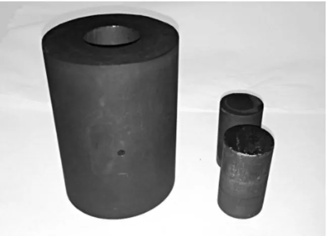
The Cu/Cu bonding was carried out with a Spark Plasma Sintering (SPS) system (FCT HPD 25). As with a classical sintering press, a SPS system applies both pressure and heat to the samples. The difference is that the heat is provided by a pulsed DC-current circulating through the graphite die (or through the sample if it is conductive), whereas the
Fig. 3. The graphite die used to bond the copper rods, with the two 20 mm-diameter pressing cylinders.
(a) (b)
Fig. 4. Shape (a) and photograph (b) of the samples used for the tensile test.
conventional sintering press uses external heating elements. As a result in the case of the SPS, the heat is generated much closer to the sample, offering very fast temperature dynamics: more than 100 K/min for the system used in this study, using current pulses of several kA.
Although not initially designed for the assembly of elec-tronic systems, the SPS technology offers interesting features: its cycle time is comparable to that of a reflow oven (a few minutes) and it operates under vacuum (avoiding oxidation of the copper). SPS systems with platens as large as 30 cm (12 in) in diameter are available, enabling the assembly of several modules at once.
In each experiment, two copper pieces were introduced in a graphite die of 20 mm inner diameter (figure 3). The bonding was performed in vacuum (10−2 torr) with
temper-atures ranging from 200 °C to 300 °C. The uniaxial force , applied during the bonding and maintained during the cooling down to room temperature, was varied from 5 kN to 24 kN (corresponding to 16 and 77 MPa on the sample respectively). The temperature was measured on the surface of the graphite die using a thermocouple.
The heating rate was fixed to 100 K/min and the holding time was varied from 5 to 20 minutes (Figure 2).
0 50 100 150 200 0.00 0.05 0.10 0.15 0.20 0.25 0.30
Engineering Stress [MPa]
Engineering Strain
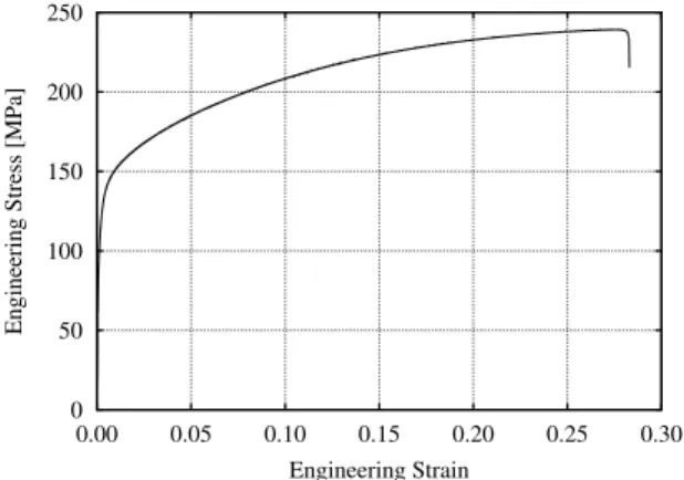
Fig. 5. Tensile test result for one of the sample (sample B in table I).
Fig. 6. Position of the experimental points in the t,T,P space
C. Characterization
After bonding the samples were machined for the mechan-ical test (tensile test), as described in figure 4. Mechanmechan-ical testing of the bonded samples was performed at room temper-ature using a Lloyd EZ20 tensile machine with a 20 kN cell force. The displacement rate was set up to 1 mm/min.
Copper being ductile, the sample quickly enters plastic deformation during the tensile test (figure 5). This results in a reduction of the actual section of the sample as it elongates. In this document, a nominal stress value is calculated using the initial surface of the tensile sample. It will thus constitute a lower bound of the true stress experimented on the sample, as plastic deformation and then necking occur before the actual rupture of the sample (hence reducing the surface of the bond). It should be mentioned that all the samples fractured along the bond line (due to the design of the sample).
Surface microstructure observations were studied by a Leitz optical microscope and a scanning electron microscope (SEM Philips XL20).
MEASUREMENT SUMMARY. AS A REFERENCE,A PLAIN COPPER SAMPLE WAS FOUND TO BREAK AT365 MPA
n° Point t (min) T (°C) P (MPa) y(stress, MPa) 1 A 5 300 77 181 2 B 20 300 77 239 3 C 20 300 16 170 4 D 5 300 16 132 5 E 5 200 77 106 6 F 20 200 77 270 7 G 20 200 16 261 8 H 5 200 16 no bond (0) 9 I 20 250 16 150 10 I 20 250 16 141 11 I 20 250 16 180 12 I 20 250 16 169 13 I 20 250 16 183
IV. PARAMETRIC ANALYSIS
A. Design of experiment approach
The cost of the experiments and the availability of the SPS equipment resulted in a limited set of assemblies. A classical 23
factorial plan [23], [24] was therefore used to study the effect of three factors (time, temperature, pressure) without making any assumption on which factors or factor combinations are significant.
This factorial plan requires 2 values to be chosen for each factor (one low and one high), resulting in 8 (23
) distinct experimental conditions. The position of these 8 points in the (t, T , P ) space is presented in figure 6. The low and high values for t have been chosen to be different enough, yet com-patible with a microelectronic assembly process. Values lower than 5 minutes would not have been sufficiently accurate. We considered that 300 °C is the maximum a semiconductor die can safely withstand. As for the pressure, 16 MPa corresponds to the pressure applied on a 20 mm-diameter sample at the minimum force setting of the press (5 kN). Note that bonding of semiconductor devices at a comparable pressure (or even higher, 40 MPa) has already been demonstrated successfully [25].
Finally, 5 additional experimental values have been acquired on a different point (I in figure 6). These points are used to evaluate the accuracy and dispersion of the experimental data. A list of the experiments, with the corresponding tensile strengths measured is given in table I
A simple linear model that takes into account all the interactions between the factors can be expressed as:
y= a0+ n X i=0 aixi+ n X i=0 n X j=i+1 ai,jxixj + n X i=0 n X j=i+1 n X k=j+1 ai,j,kxixjxk+ . . . (1)
For a 3-factor case, this can be simplified to y= a0+ a1x1+ a2x2+ a3x3+ a1,2x1x2
+ a1,3x1x3+ a2,3x2x3+ a1,2,3x1x2x3
(2) Where x1, x2and x3are the normalized factors, corresponding
by the sample at the breaking point. The normalization of a factor (or parameter) p is calculated as:
xi= p − pmax+pmin 2 pmax−pmin 2 (3) With pmin and pmax the low and high values of the factor p
respectively. The normalized values (1, -1, or 0) of t, T and P are given for each point in figure 6.
The model in eq. (2) requires 8 parameters (a0. . . a1,2,3) to
be identified. This model can be expressed as:
y= M · a (4) Where y is the column matrix that contains the tensile strengths for points A to H (see table I), a the column matrix that contains the parameters a0. . . a1,2,3 to be calculated and
M a matrix that contains the values of the 3 factors and their combinations, for each of the 8 experimental points. Each row of M corresponds to the coefficients of (2): x0
(constant factor associated with a0 in eq. (2), always equal
to 1), x1 (normalized factor t), x2 (T ), x3 (P ), x1x2, x1x3, x2x3, x1x2x3: yA yB yC yD yE yF yG yH = 1 −1 1 1 −1 −1 1 −1 1 1 1 1 1 1 1 1 1 1 1 −1 1 −1 −1 −1 1 −1 1 −1 −1 1 −1 1 1 −1 −1 1 1 −1 −1 1 1 1 −1 1 −1 1 −1 −1 1 1 −1 −1 −1 −1 1 1 1 −1 −1 −1 1 1 1 −1 · a0 a1 a2 a3 a1,2 a1,3 a2,3 a1,2,3 (5)
As MT · M = nI, with n the size of the matrix M (in our case, n= 8), a can be calculated as:
a= 1 nM
Ty
(6) An expanded version of (6) for n = 8 is given in (7), with yA. . . yH the tensile stress measured for points A . . . H
respectively. The calculated values of a0to a1,2,3 are listed in
table II.
B. Model accuracy
5 samples were assembled at the same experimental point I (see table I) in order to characterize the reproducibility and accuracy of the bonding process and of the tensile tests. From these measurements, a tensile strength value of 164.4±20% was calculated for point I.
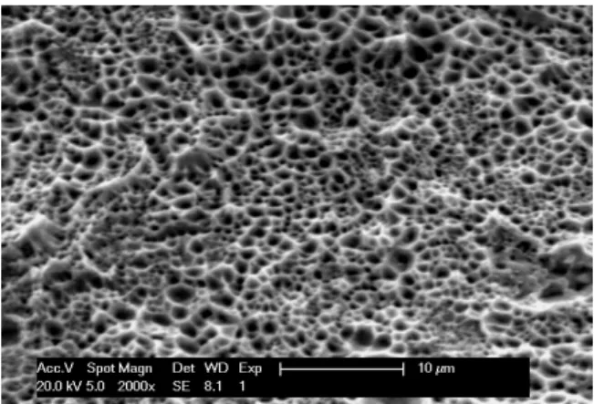
Fig. 8. SEM image of the fracture surface (after tensile test), for a sample bonded at 300 °C for 20 minutes and with a pressure of 16 MPa.
This fairly large tolerance is due to the low sample count, as well as to the low reproducibility of the tensile tests: a much bigger number of samples is usually required but this was unpractical in our case.
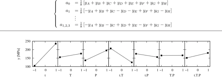
A diagram of the influence of each factor is given in figure 7. This diagram is obtained by using the data in table I (points A to H). For each sub-graph, two data set are formed (one for both values of the corresponding factor, i.e 1 or -1), and the average value of y is calculated for each set. As an example, for the first sub-plot (t), the two dataset correspond to t =5 min (points A, D, E, H) and 20 min respectively (points B, C, F, G).
Considering the ±20% accuracy, only few parameters in table II are significant: a0 (the average tensile strength for all
samples), a1 (effect of time), a3 (effect of the pressure) and
a1,2(conjugated effect of time and temperature).
Therefore, the model (2) can be simplified as: y = a0+ a1x1+ a3x3+ a1,2x1x2
= 166 + 65x1+ 29x3− 41x1x2 (8)
Applying this model to the parameters of point I in table I (t = 20 min, T = 250°C, P = 16 MPa, or x1 = 1,
x2 = 0, x3 = −1 respectively), yields a tensile strength of
202±40 MPa. This is compatible with the tensile strength measured at point I (164.4±20%), but the precision of the results is too low to conclude about the suitability of our linear model. More data points would be needed to improve the accuracy.
V. DISCUSSION
Even with the limited variation range for all three factors (5-20 minutes, 200–300 °C, and 16–77 MPa), substantial differences were found in tensile strength. In most cases, however, a very good bond was formed: the tensile strength of the used bulk copper-rod was found to be 365 MPa, while most results in table I are over 122 MPa (a third of the bulk value).
Another evidence of the good bond quality is visible in figure 8: the fracture surface is characteristic of ductile fracture with the presence of dimples. This means that the sample has been heavily deformed, which is also exhibited by the large
a1 =18[−yA+ yB+ yC− yD− yE+ yF+ yG− yH] .. . a1,2,3 =18[−yA+ yB− yC+ yD+ yE− yF+ yG− yH] (7) 100 150 200 250 −1 0 1 y [MPa] t −1 0 1 T −1 0 1 P −1 0 1 t.T −1 0 1 t.P −1 0 1 T.P −1 0 1 t.T.P
Fig. 7. Influence of the factors time (t), temperature (T ), pressure (P ) and their interactions on the tensile strength y. This shows that the most important factors are the time, pressure, and the interaction between time and temperature (t,T).
(a) (b) (c)
Fig. 9. EBSD pictures of three samples captured just below the bonding line, with the samples standing upright, bonded for 20 minutes, under a pressure of 16 MPa, and a temperature of 200°C (a), 250°C (b) and 300°C (c). This shows a much bigger grain size for the sample bonded at 200°C (101 µm average) than for 250°C (46 µm) or 300°C (50 µm).
strain value attained during the tensile tests (as can be seen for example in figure 5). Similar patterns were found over the entire fracture surface and for all samples.
From the model in (2), it can be seen that time (x1) and
pressure (x3) have the expected effect: an increase in either
of these parameters results in a stronger bond.
The negligible influence of temperature and the negative effect of the simultaneous increase of time and temperature can firstly be surprising, but can actually be explained by the following considerations: in these tests, a good bond could be achieved for any temperature or time value. However, the application of temperature to the samples also constitutes a heat treatment of the copper. The effect of such treatment on work hardened copper is a change in its microstructure. For example, increasing the temperature from 200 °C to 300 °C would involve further annealing and recrystallization of the sample, decreasing its overall mechanical properties. This point is beyond the scope of this paper, but the Electron Backscatter Diffraction (EBSD) images shown in figure 9
Fig. 10. Example of a micropost bonded onto a DBC substrate. This post is part of a diode-to-DBC bonding experiment in which the interface between the posts and the diode was found to be defective. The copper-to-copper bond, however, is of very good quality. The bond line only visible at the edges of the assembly.
demonstrate that the crystallographic structure of the copper changes with the bonding parameters. Therefore, the decrease in mechanical strength is mainly caused by the reduction in the intrinsic mechanical properties of the copper rather than by the bond itself. This is confirmed by the ductile fracture surfaces observed on all samples.
Finally, a test structure comprising a silicon power diode (12.7×12.7 mm die size) with copper posts electroplated on one side, placed between two DBC substrates, was assembled. This test structure comprises two insulating layers (the ceramic layers of the DBCs). The voltage applied by the SPS equip-ment is in the order of 4 V, much lower than the dielectric strength of the ceramic layers (several kilovolts). Therefore, it was expected that the path of the heating current in the SPS press would differ dramatically from the conductive (copper) samples in figure 4(b). As a result, this could have a strong effect on the bonding.
The copper posts were successfully bonded on the copper layer of the DBC (a close-up cross-section is shown in figure 10). However, the post-to-die interface was found to be weak and failed, which is why no diode is visible in the figure. This issue is related to the processes prior to the copper plating, and is therefore beyond the scope of this paper. It
is compatible with the requirements of the application: a semiconductor die can sustain temperatures up to 300°C for a few minutes and pressures in the order of a few tens of MPa. A bonding strength higher than previously reported in the literature was found (between a third and more than two thirds of the bulk copper tensile strength). Furthermore, this good bond was obtained for temperatures as low as 200°C. A study is currently being carried out to understand the physics of this bonding process. In particular, the effect of the intense electrical current used for the SPS heating is under investigation.
Based on this bonding technique, a “sandwich” structure comprising a silicon die and two DBC substrates was assem-bled. A bond was observed between the copper posts of the die and the copper of the DBC, even with the ceramic layers of the substrates forming an electrical insulation around the parts to be bonded. This proves the feasibility of the technique for 3D packaging applications.
ACKNOWLEDGMENT
The authors would like to thank the Agence Nationale de la Recherche for their financial support of this work under the project grant ECLIPSE.
They are also pleased to acknowledge important contribu-tions used in the body of this work from G. Bonnefont and F. Mercier from MATEIS for SPS processing, as well as to thank M. Perez from MATEIS for fruitful discussions.
REFERENCES
[1] A. Hamidi and D. Cottet, “Parasitics in power electronics packaging,” in 37thInternational Symposium on Microelectronics, IMAPS. Long
Beach, California, USA: IMAPS, nov 2004.
[2] S. Dieckerhoff, T. Kirfe, T. Wernicke, C. Kallmayer, A. Ostmann, E. Jung, B. Wunderle, and H. Reichl, “Electric Characteristics of Planar Interconnect Technologies for Power MOSFETs,” in Power Electronics Specialists Conference, 2007. PESC 2007. IEEE, jun 2007, pp. 1036 –1042.
[3] P. Ning, T. Lei, F. Wang, G.-Q. Lu, and K. Ngo, “A Novel High-Temperature Planar Package for SiC Multi-Chip Phase-Leg Power Module,” in Applied Power Electronics Conference and Exposition, 2009. APEC 2009. Twenty-Fourth Annual IEEE, feb 2009, pp. 2061 –2067.
[4] C. Gillot, C. Schaeffer, C. Massit, and L. Meysenc, “Double-Sided Cooling for High Power IGBT Modules Using Flip Chip Technology,” IEEE Transaction on Components and Packaging Technology, vol. 24, no. 4, pp. 698–704, dec 2001.
[5] C. Buttay, J. Rashid, C. Johnson, F. Udrea, G. Amaratunga, P. Ireland, and R. Malhan, “Compact Inverter Designed for High-Temperature Operation,” in Proc. IEEE Power Electronics Specialists Conference PESC 2007, 2007, pp. 2241–2247.
[6] R. Markus, A. Schletz, and M. M¨arz, “Study on Advanced cooling with focus on double-sided cooling,” ECPE, ECPE e.V. Landgrabenstr. 94 90443 N¨urnberg, technology survey, juil 2008. [Online]. Available: www.ecpe.org
Power Electronics, vol. 25, no. 7, pp. 1667–1670, jul 2010.
[10] W. W. Sheng and R. P. Colino, Power Electronic Modules: Design and Manufacture, 1st ed. CRC, jun 2004.
[11] K. Guth, D. Siepe, J. G¨orlich, H. Torwesten, R. Roth, F. Hille, and F. Umbach, “New assembly and interconnects beyond sintering meth-ods,” in Proceedings of PCIM, Nuremberg, may 2010, pp. 232–237. [12] T. Nitta, T. Ohmi, T. Hoshi, S. Sakai, K. Sakaibara, S. Imai,
and T. Shibata, “Evaluating the Large Electromigration Resistance of Copper Interconnects Employing a Newly Developed Accelerated Life-Test Method,” Journal of The Electrochemical Society, vol. 140, no. 4, pp. 1131–1137, 1993. [Online]. Available: http://link.aip.org/link/ ?JES/140/1131/1
[13] P.-L. Pai and C. Ting, “Selective electroless copper for VLSI intercon-nection,” Electron Device Letters, IEEE, vol. 10, no. 9, pp. 423 –425, sep. 1989.
[14] A. Fan, A. Rahman, and R. Reif, “Copper Wafer Bonding,” Electrochemical and Solid-State Letters, vol. 2, no. 10, pp. 534–536, 1999. [Online]. Available: http://link.aip.org/link/?ESL/2/534/1 [15] K. Chen, C. Tan, A. Fan, and R. Reif, “Copper bonded layers
analysis and effects of copper surface conditions on bonding quality for three-dimensional integration,” Journal of Electronic Materials, vol. 34, pp. 1464–1467, 2005, 10.1007/s11664-005-0151-0. [Online]. Available: http://dx.doi.org/10.1007/s11664-005-0151-0
[16] Y. A. Li, R. W. Bower, and I. Bencuya, “Low Temperature Copper to Copper Direct Bonding,” Japanese Journal of Applied Physics, vol. 37, no. Part 2, No. 9A/B, pp. L1068–L1069, 1998. [Online]. Available: http://jjap.jsap.jp/link?JJAP/37/L1068/
[17] K.-N. Chen, A. Fan, and R. Reif, “Microstructure examination of copper wafer bonding,” Journal of Electronic Materials, vol. 30, pp. 331–335, 2001, 10.1007/s11664-001-0039-6. [Online]. Available: http://dx.doi.org/10.1007/s11664-001-0039-6
[18] H. Takagi, K. Kikuchi, R. Maeda, T. R. Chung, and T. Suga, “Surface activated bonding of silicon wafers at room temperature,” Applied Physics Letters, vol. 68, no. 16, pp. 2222–2224, 1996. [Online]. Available: http://link.aip.org/link/?APL/68/2222/1
[19] H. Takagi, R. Maeda, N. hosoda, and T. Suga, “Transmission Electron Microscope Observations of Si/Si Interface Bonded at Room Temperature by Ar Beam Surface Activation,” Japanese Journal of Applied Physics, vol. 38, no. Part 1, No. 3A, pp. 1589–1594, 1999. [Online]. Available: http://jjap.jsap.jp/link?JJAP/38/1589/
[20] T. H. Kim, M. M. R. Howlader, T. Itoh, and T. Suga, “Room temperature Cu–Cu direct bonding using surface activated bonding method,” Journal of Vacuum Science & Technology A: Vacuum, Surfaces, and Films, vol. 21, no. 2, pp. 449–453, 2003. [Online]. Available: http://link.aip.org/link/?JVA/21/449/1
[21] J. W. Elmer, J. Klingmann, and K. Van Bibber, “Diffusion bonding and brazing of high purity copper for linear collider accelerator structures,” Phys. Rev. ST Accel. Beams, vol. 4, no. 5, p. 053502, May 2001. [22] A. He, T. Osborn, S. A. Bidstrup Allen, and P. A. Kohl,
“Low-Temperature Bonding of Copper Pillars for All-Copper Chip-to-Substrate Interconnections,” Electrochemical and Solid-State Letters, vol. 9, no. 12, pp. C192–C195, 2006. [Online]. Available: http: //link.aip.org/link/?ESL/9/C192/1
[23] P. Dagnelie, Principes d’exp´erimentation – Planification des exp´eriences et analyse de leurs r´esultats, electronic edition, in french ed. Gembloux: les presses agronomiques de Gembloux, 2003. [Online]. Available: http://www.dagnelie.be
[24] L. Dascalescu, K. Medles, S. Das, M. Younes, L. Caliap, and A. Mi-halcioiu, “Using Design of Experiments and Virtual Instrumentation to Evaluate the Tribocharging of Pulverulent Materials in Compressed-Air Devices,” IEEE Transactions on Industry Applications, vol. 44, no. 1, pp. 3–8, jan 2008.
[25] C. G¨obl, P. Beckedahl, and H. Braml, “Low temperature sinter technology Die attachment for automotive power electronic applications,” in Automotive Power Electronics, Paris, 21–22 jun 2006,