Chemically Driven Interfacial Coupling in
Charge-Transfer Mediated Functional Superstructures
The MIT Faculty has made this article openly available.
Please share
how this access benefits you. Your story matters.
Citation
Xu, Beibei et al. “Chemically Driven Interfacial Coupling in
Charge-Transfer Mediated Functional Superstructures” Nano Letters 16, 4
(April 2016): 2851–2859 © 2016 American Chemical Society
As Published
http://dx.doi.org/10.1021/ACS.NANOLETT.6B00712
Publisher
American Chemical Society (ACS)
Version
Author's final manuscript
Citable link
http://hdl.handle.net/1721.1/111824
Terms of Use
Article is made available in accordance with the publisher's
policy and may be subject to US copyright law. Please refer to the
publisher's site for terms of use.
Chemically Driven Interfacial Coupling in Charge-Transfer Mediated
Functional Superstructures
Beibei Xu,
†Huashan Li,
‡Haoqi Li,
†Andrew J. Wilson,
§Lin Zhang,
†Ke Chen,
∥Katherine A. Willets,
§Fei Ren,
†Jeffrey C. Grossman,
*
,‡and Shenqiang Ren
*
,††Department of Mechanical Engineering and Temple Materials Institute, Temple University, Philadelphia, Pennsylvania 19122,
United States
‡Department of Materials Science and Engineering, Massachusetts Institute of Technology, Cambridge, Massachusetts 02139 United
States
§Department of Chemistry, Temple University, Philadelphia, Pennsylvania 19122, United States
∥Department of Physics and Temple Materials Institute, Temple University, Philadelphia, Pennsylvania 19122, United States
*
S Supporting InformationABSTRACT: Organic charge-transfer superstructures are enabling new interfacial electronics, such as organic thermoelectrics, spin-charge converters, and solar cells. These carbon-based materials could also play an important role in spin-based electronics due to their exceptionally long spin lifetime. However, to explore these potentials a coherent design strategy to control interfacial charge-transfer interaction is indispensable. Here we report that the control of organic crystallization and interfacial electron coupling are keys to dictate external stimuli responsive behaviors in organic charge-transfer superstructures. The integrated experimental and computational study reveals the importance of chemically driven interfacial coupling in organic charge-transfer superstructures. Such degree of engineering opens up a new route to develop a new generation of functional charge-transfer materials, enabling important advance in all organic interfacial electronics.
KEYWORDS: Nanoferroics, organic crystallization, materials design, and multifuctionality
T
he mixing of conductivity and ferroic orders in functional materials could lead to numerous technological advances, such as ferroic field-effect transistors and magnetoelectric tunnel junctions.1−4However, the ferroic orders are related to the interaction of localized electrons while the conduction is determined by the movement of electrons; thus, simultaneous conducting and ferroic orders remains challenging in conven-tional materials. Materials-by-design and assembly principle provides a unique and exciting opportunity, as it allows us to design novel multifunctional organic materials that combine two or more physical properties in the same crystal lattice, which are difficult or impossible to achieve in continuous inorganic crystalline solids. Organic charge transfer (CT) assemblies, consisting of an electron donor and acceptor with π-electron orbitals, can possess both charge and spin orders due to the largely delocalized π-electrons and the exchange interaction.5,6 Over the past decades, numerous materials have been designed toward the development of functional CT complexes.7,8 Recently, room-temperature multiferroicity in centimeter-sized crystalline charge-transfer superstructures, consisting of polymer−fullerene complexes, was achieved by the self-organization and molecular-packing induced charge order-driven ferroic coupling.9 To take advantage of the complexity and tunability of this new class of organic functionalmaterials, a comprehensive understanding of the relationship between structure and properties is important.
Interfacial engineering has been widely used to tune the electronic and optical behaviors of polymer−fullerene-based CT devices, and materials-by-design criteria exhibit a strong dependence on their structural architecture as demonstrated by both experimental10−14and theoretical15−19studies. Typically, longer side chain lengths of polymers lead to higher fullerene mobility and thus a larger scale of phase separation that reduces the interfacial area for charge separation.20Despite the novel properties observed in polymer−fullerene-based CT structures, a systematic analysis regarding the design strategy of polymer side-chain engineering is lacking. The conclusions obtained by previous studies on blendfilms cannot necessarily be applied to the CT superstructures because (1) although diffusion of C60 molecules is important to determine the morphology of traditional blends, it is a negligible effect in the CT superstructures as the C60s are packed inside the crystal
domains; (2) unlike the relatively fixed donor−acceptor distance in traditional blends with the π-stacking direction perpendicular to the interface,17 the lengths of side-chains Received: February 18, 2016
Letter
pubs.acs.org/NanoLett
© XXXX American Chemical Society A DOI:10.1021/acs.nanolett.6b00712
determine the donor−acceptor distances in the CT super-structures as the π-stacking direction is nearly parallel to the interface, and thus may substantially affect the electron coupling for charge transfer and intersystem crossing. In this work, we shed light on the impact of chemically driven side-chain engineering on correlated optical, thermal, electric and magnetic properties of CT superstructures using a combined experimental and theoretical approach. The CT superstructures with crystallization between fullerene (C60) acceptor and
polythiophene donor with varying alkyl side chains were chosen as prototype systems since exceptional optoelectronic response and optical characteristics have been observed in these π-conjugated systems.21,22
Our results suggest that the essential strategy for side-chain design to dictate external stimuli
responsive behavior is control over polymer crystallization and interfacial electron coupling. Moreover, the Seebeck coefficients observed in such CT superstructures are among the highest reported for polymeric thermoelectric materials.
In order to probe the effect of alkyl side-chain length on donor−donor and donor−acceptor couplings, we examine the following electron donors: poly(3-butylthiophene-2,5-diyl) (BT), hexylthiophene-2,5-diyl) (HT), and poly(3-dodecylthiophene-2,5-diyl) (DDT) with side chains consisting of 4, 6, and 12 carbon alkyls, respectively (shown in the inset of
Figure 1a−c). The antisolvent crystallization combined with the solvent vapor evaporation approach is employed to obtain the CT superstructures. In comparison to the randomly distributed particle-like formation of BT-C60 complex (Figure 1a and Figure 1. Crystal structure, morphology, chemical analysis of charge transfer complexes, and microscopic structural information on CT superstructures. (a−c) SEM and EDS element map of BT-C60, HT-C60, and DDT-C60complexes, respectively. The insets are the structural formula
of BT, HT, DDT and fullerene (C60). The scale bars in panels a−c are 10, 50, and 30 μm, respectively. (d−f) Snapshot of disordered BT-C60,
crystallized HT-C60, and crystallized DDT-C60interfaces at t = 1 ns, respectively. C60, green; C in P3XT, blue; S in P3XT, yellow. (g,h) Probability
density function of distance between nn rings in polymer phases and between rings and nn C60 molecule at BT-C60, HT-C60, and DDT-C60
interfaces, respectively. (i,j) Evolution of averaged ring-C60distance after early time stage of NPT simulations with those during early time stage
shown in the inset, and minimum ring-C60distance after early time stage, respectively.
Nano Letters Letter
DOI:10.1021/acs.nanolett.6b00712
Nano Lett. XXXX, XXX, XXX−XXX
Figure S2), the HT-C60and DDT-C60 complexes enable
well-defined needle-like crystal formation (Figure 1b,c, andFigure S3−S4). Figure 1a−c shows scanning electron microscopy (SEM) images and the carbon and sulfur chemical analysis mapping from energy dispersive X-ray spectroscopy (EDS) of BT-C60, HT-C60, and DDT-C60, respectively, in which the
phase identification is confirmed by X-ray diffraction (XRD,
Figure S1). On the basis of the insights from these crystal structure measurements, we further probe the origin of
microscopic crystalline formation of these superstructure phases using classical molecular dynamics (MD) (the detailed simulation methods are described in the Supporting Informa-tion Section 5.1). Because of the strong attraction between molecules inside each phase and the steric repulsion between polymer side-chains and C60 molecules, phase separations are
stable regardless of the degree of crystallization of the polymers during the 1 ns simulations within the isothermal−isobaric (NPT) ensemble, as shown inFigure 1d for disordered BT and Figure 2.Optical properties of charge transfer complexes. (a) Absorption spectra of BT-C60, HT-C60, and DDT-C60complexes. (b) HOMO (in
cyan) and LUMO (in magenta) wave functions of the pair of truncated polymer and C60molecule with the side-chains perpendicular to the interface.
(c) Calculated absorption spectra of BT, HT, and DDT crystals. (d,e) Calculated donor−acceptor distance-dependent absorption spectra of pairs of truncated polymers and C60molecules associated with charge transfer states with the side-chains parallel (d) and perpendicular (e) to the interface.
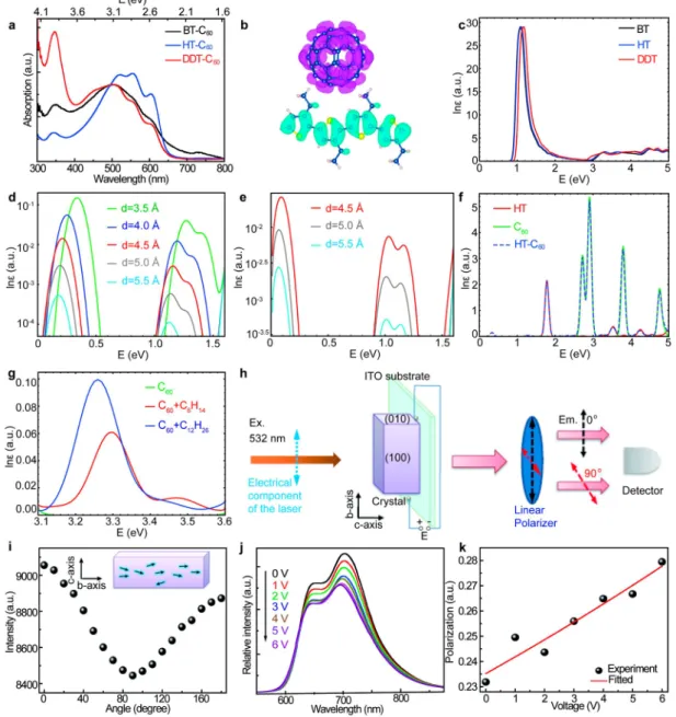
(f) Comparison of calculated absorption spectra between the combined system shown in (b) and its isolated components. (g) Calculated absorption spectra relevant to charge transfer states at the interfaces between a C60molecule and an alkyl chain containing 6/12 C atoms. (h) Scheme for the
fluorescence measurements with an applied voltage. The electric component of the excitation laser is parallel to the crystal growth direction. The emission light is detected through a polarizer set to an angle of 0° or 90° with respect to the electric component of the excitation laser. Electrical leads are attached such that the voltage is applied along the b-axis of the crystal. The actualfluorescence experiment is performed in a backscattering configuration but is drawn as forward scattering for clarity. (i) Excitation polarization (0°−180°) dependent fluorescence intensity of the HT-C60
crystal. The values of 0° and 90° correspond to the b-axis and a-axis of HT-C60crystal, respectively. The small arrows in the crystal denote dipoles.
(j) Electric field-dependent photoluminescence for the 0° emission of the HT-C60 crystal. (k) The polarization ratio change for the emission
intensity at 700 nm. The ratio increases with an increase of applied voltage. The voltage is applied parallel to the crystal growth direction.
Nano Letters Letter
DOI:10.1021/acs.nanolett.6b00712
Nano Lett. XXXX, XXX, XXX−XXX
Figures 1e,f for ordered HT/DDT, respectively. The distances between nearest neighboring (nn) five-member rings are slightly larger in DDT than in HT, whereas a much broader profile is observed in disordered BT (Figure 1g). Starting from a spacing of about 0.3 nm, the polymer−C60 interfacial
structures relax quickly within 10 ps and evolve very slowly afterward (Figure 1i). The distances between rings and their nn C60 molecules at the DDT-C60 interface are much larger than those at the HT-C60 interface but follow a similar Gaussian
distribution.9By contrast, the ring-C60 distance distribution at
the disordered BT-C60interface is much broader and irregular,
with a larger proportion in small distances that tends to increase with increasing time (Figure 1h and Figure S12). While the head-to-head defects at the polymer−C60 interface
also increase the probability of short ring-C60 distances, the effect is much less significant than the disordered initial condition (Figure S14). These results provide a qualitative scenario of how the modification of side-chain chemistry affects the microscopic structure in two aspects, the crystallization of the polymer and the donor−acceptor distance. Next we focus on how such subtle changes in microscopic structure result in a wide range of physical properties.
Figure 3.Electron transport properties. (a) Calculated electron coupling between truncated P3HT with different π-stacking distance. (b) Calculated Δz (shift between neighboring polymers along the backbone direction) dependent electron coupling between truncated polythiophene molecules containing eight rings. (c) Computed total energy variation of polythiophene crystals versusΔz referred to zero-shift configuration. (d) Calculated electron coupling (in units of meV) dependent hole mobility for the polythiophene crystal phases and electron mobility for the C60phase. (e)
Experimental conductivity of BT-C60, HT-C60, and DDT-C60complexes with alkyl side chain containing 4, 6, and 12 carbon alkyls. (f) AFM and
conducting AFM of BT-C60, HT-C60, and DDT-C60 complexes, respectively. (g) Effect of side chain length on the room temperature Seebeck
coefficient of BT-C60, HT-C60, and DDT-C60complexes, respectively. The inset is the measurement scheme of thermoelectric effect.
Nano Letters Letter
DOI:10.1021/acs.nanolett.6b00712
Nano Lett. XXXX, XXX, XXX−XXX
Although the alkyl side chains are electronically inert, the measured absorption spectra for BT-C60, HT-C60, and
DDT-C60 complexes are remarkably different from one another as
shown in Figure 2a. To understand this phenomenon, we compute the absorption spectra of crystallized polymers with infinite lengths, and pairs of truncated polymer and C60
molecules, by ab initio simulations using the random phase approximation (RPA). Although RPA does not accurately predict the optical gaps, it gives a similar strength of CT absorption to those obtained by the more accurate GW-BSE method in previous studies on HT-C60 interfaces
23
and thus serves as a sufficient method for our purpose of qualitatively identifying the origin of absorption peaks. Because the calculated spectra for crystallized polymers exhibit only slight variations of near-edge absorption caused by different stacking distances, the strongest absorption at 450−600 nm observed in HT-C60 is likely due to the highest packing density, while the
broadening of the absorption peak can be ascribed to the wide range of conjugation lengths in the disordered system. Notice that only BT-C60 provides absorption peaks in the infrared
range, which may originate from the direct generation of CT states as illustrated in Figure 2d−f. Such excitation requires sufficient electron coupling between the highest occupied molecular orbital (HOMO) localized on the polymer and the lowest unoccupied molecular orbital (LUMO) localized on C60
(Figure 2b), which decays sharply with increasing donor− acceptor distance (Figure 2d,e,Supporting InformationSection 5.3) and thus can only occur in disordered BT-C60 super-structures with unique donor−acceptor separation profiles. The broad absorption spectrum of the BT-C60 complex reveals
enhanced charge transfer interaction (Figure 2a), resulting from the short side chain enhancedπ-electron density and decreased shielding effects from donating electrons to acceptors.24 In addition, the strong UV absorption in the DDT-C60
super-structures can be understood from the alkyl chain related transitions either within the polymer (Figure 2c) or at the donor−acceptor interface (Figure 2g). The effect of the alkyl
side chain on molecular packing can influence the optical anisotropy of CT crystalline superstructures. The 532 nm excitation light polarization is rotated in 10° increments with respect to the crystal growth axis (defined as 0°) and the resulting emission intensity is measured (Figure 2h).Figure 2i shows the representative data for a HT-C60crystal in which the
fluorescence intensity reaches a maximum (minimum) when the excitation polarization is parallel (perpendicular) to the crystal growth axis, indicating a slight preferential alignment of the transition dipoles along the direction of the crystal growth. The emission is also slightly polarized in this sample, as determined by aligning the excitation polarization along the b-axis of the crystal (e.g., 0°) and collecting the fluorescence emission polarized either parallel or perpendicular to the excitation (Figure S6a). These results are consistent with the previous report that the polythiophene−C60 CT
super-structures are self-organized through the π−π conjugated interaction along the b-axis (crystal growth direction) and stacked in planar structures with the long chain axis (c-axis) nearly perpendicular to the substrate.9 While thefluorescence emission is also polarized for the DDT-C60crystal, the BT-C60
crystal shows no preferential emission polarization, consistent with the disordered nature of this material (Figure S6e,f). Furthermore, the change influorescence from a single HT-C60 crystal measured as an external electric potential is applied. The excitation polarization isfixed parallel to the crystal’s b-axis and
thefluorescence is collected through a linear polarizer set either parallel (0°) or perpendicular (90°) with respect to the excitation (Figure 2h). Figure 2j,k shows the external electric potential-dependent emission of a HT-C60 crystal. As the electricfield increases, the emission intensity at both 0° and 90° decreases (Figure 2j and Figure S7, respectively), which we attribute to the increased dissociation of excitons at the CT interface. The polarization ratio (P) is then calculated from the intensity of the emission at 700 nm, polarized either parallel (I0) or perpendicular (I90) as follows = − + P I I I I ( ) ( ) 0 90 0 90 (1)
The polarization ratio increases linearly with applied voltage, indicating that anisotropic emission can be induced in these materials through application of an applied field (Figure 2k).
The side-chains of polythiophene are also known to play a critical role in the carrier transport.10,12,14Though both density functional theory (DFT) and molecular dynamics (MD) simulations have been implemented to probe the electronic structure and packing order of HT crystals,18,19,25the atomistic-scale understanding of how the side-chains affect the carrier mobility has received less attention. To address this potential, we apply the phonon-assisted charge transfer model with a full quantum treatment,26,27wherein the hopping rate is dictated by the electron coupling and reorganization energy (Supporting IinformationSection 5.4). The most straightforward side-chain effect is increasing π-stacking distance with increasing side chain length,28 which results in a weak electron coupling (Figure 3a). Though the shift between neighboring polymer along the backbone direction (Figure 3b) is weak, it can still substantially reduce the electron coupling caused by insufficient wave function overlap (Figure 3c). Interestingly, the energy profile versus shift distance exhibits a nonmonotonic trend with side-chain length (Figure 3c), which can be explained by the fact that the deviation from ideal crystal structure reduces the steric repulsion between nn ligands but increases the steric energy between dentate units. In addition to the local effects, side-chains also change the crystallinity of the polymer and thus the conjugation length. As summarized in Table 1, electron
coupling (V) is insensitive to the conjugation length (Lc) if the positions of the conjugating domains are close to each other, yet a larger Lc generally favors the overlap of conjugating domains. In contrast, the reorganization energy (λ) correspond-ing to the electron−phonon coupling strength decreases sharply with increasing Lc, which results in a lower effective hopping barrier. These influences can be mapped onto the carrier mobility (μ) with μ increasing with decreasing λ and increasing V (Figure 3d). As defects have not been accounted for in this treatment, and the degree of irregularity in a realistic system is higher than that in our model, our calculated mobility is in reasonable agreement with experimental values (0.1−0.5 cm2V−1s−1).10,29
Moreover, in response to various population Table 1. Electronic Coupling (V) between Two Truncated Polymers and Reorganization Energy (λ) of Hole Hopping with Various Conjugation Lengths (Lc)
Lc (rings) V (meV) λ (meV)
6 140.5 152.0
8 136.2 110.4
10 133.6 90.2
Nano Letters Letter
DOI:10.1021/acs.nanolett.6b00712
Nano Lett. XXXX, XXX, XXX−XXX
distributions of phonon modes, the mobilityfirst increases then decreases with increasing temperature, which is consistent with the negative temperature dependence reported for P3HT near room temperature.29 The calculated mobility for C60 is also
consistent with experimental values of 0.3−6 cm2V−1s−1,30,31 implying that it is possible to achieve charge balance between donor and acceptor by tuning the donor side-chains. These calculations are consistent with our experimental results that HT provides the highest robustness against shift and thus may lead to large electron coupling, which is evidenced by the largest conductivity for HT-C60in comparison to the other two (Figure 3e and Figure S9). The side-chain dependent steric hindering effect on the effect of conductivity is also confirmed by the conducting AFM (c-AFM, Figure 3f), where the segregation between the DDT-rich donor phase and C60-rich
acceptor phase is larger than that of the other two (Figure 3f). To further confirm the polymeric crystallization and interfacial electron coupling effect, the side-chain dependent thermo-electric Seebeck coefficient is shown in Figure 3g. At room temperature, Seebeck coefficients of HT-C60and DDT-C60are
190± 10 and 110 ± 40 μV/K, respectively, while no detectable thermovoltage is measured from the BT-C60. The Seebeck
coefficients observed in HT-C60crystals are among the highest
reported for polymeric thermoelectric materials, which typically
ranged between tens to hundreds of microvolt per kelvin (Table S2).32−38 It is known that bipolarons are the major charge carriers in doped polythiophenes.39,40 As proposed by Bubnova et al., the Fermi levels, EF, of amorphous bipolaron
conducting polymers lies between the valence band and the bipolaron band, and the density of states (DOS) near EFvaries
very little with respect to energy.41As the ordering increases, the bipolaron band starts to merge into the valence band and becomes empty, resulting in an increase in the DOS slope near EF. Because the Seebeck coefficient is related to the slope of the
DOS at EF,42one would expect that increase in the crystallinity of bipolaron conducting polymers can lead to an enhanced Seebeck coefficient.
The relatively small dielectric constant in organic materials is beneficial for the formation of a large Coulomb capture radius with the generation of the CT state.43An external magnetic field can cause spin-mixing with the change of the ratio between singlet and triplet CT state, leading to the change of corresponding CT dependent properties.44As shown inFigure 4a andFigure S6, the emission intensity of the BT-C60complex
increases under an external magneticfield of 100 mT due to the induced triplet to singlet conversion, whereas it decreases for both HT-C60 and DDT-C60 crystals, suggesting the transfer of singlet to triplet CT state. We evaluate the magneto-Figure 4.External stimuli control of optical, electrical, and ferroic properties. (a) Photoluminescence change for BT-C60, HT-C60, and DDT-C60
complexes without magneticfield and with magnetic field of 100 mT, respectively. (b) MC for BT-C60, HT-C60, and DDT-C60complexes under
different magnetic field. The applied electric field is 233 kV/cm. The inset is the measurement scheme of MC. (c) Frequency-dependent dielectric constant of HT-C60 crystal. The inset is the temperature-dependent dielectric constant change for HT-C60 crystal. (d) Magneticfield-dependent
dielectric constant change for HT-C60 crystal at a frequency of 100 Hz. (e) Electron spin resonance spectra of HT-C60 under dark and light
illumination at 100 mW/cm2. The inset is the light intensity dependent susceptibility change for BT-C
60, HT-C60, and DDT-C60 complexes. (f)
Magnetoelectric coupling coefficient change for BT-C60, HT-C60, and DDT-C60complexes under a electricfield of 700 V/cm. The light intensity is
70 mW/cm2. The magneticfield is 60 Oe.
Nano Letters Letter
DOI:10.1021/acs.nanolett.6b00712
Nano Lett. XXXX, XXX, XXX−XXX
conductance (MC) to gain further understanding of the CT characters in the complex with different side chain length.
Figure 4b and Figures S25−S34 demonstrate a negative MC under different external stimuli (the inset illustrates the measurement scheme of MC). The scattering reaction between triplet CT states and polarons decreases the mobility of polarons, resulting in the decrease of the current density under magnetic field within the HT-C60 and DDT-C60 crystals,
deemed as the negative MC effect. The magnetic field induces a decrease of the triplet CT by transferring them to the singlet CT, leading to the negative MC effect with a decrease of the charge carrier density. As discussed in Figure 1, a short alkyl side chain benefits the formation of CT states and thus the HT-C60 crystal exhibits a larger MC than that of the DDT-C60 crystal. However, a relatively small MC effect is shown in the BT-C60 complex, which results from its lower crystallinity. In the CT complex, the collective electron transfer from donor to acceptor leads to the formation of dipoles, which can be tuned by external stimuli. The ordered noncentrosymmetric crystal-line structure with the generation of long-range orientation of dipoles, and the large density of CT states are beneficial for organic CT ferroelectrics.45,46It is consistent with the results in the inset ofFigure 2j that the loading of electric field increase the alignment of the dipoles toward the crystal growth direction. The HT-C60 crystal exhibits the optimum
photo-excitation dependent polarization due to its ordered structure and relatively weak shielding effect from donating electrons to acceptors (Figure S34a). In addition, its dielectric constant decreases with increasing frequency due to the dielectric relaxation (Figure 4c). The HT-C60 crystal shows a large
dielectric constant at low frequency, while the BT-C60complex
shows a small dielectric relaxation due to the short alkyl side chain induced relatively large CT density. The inset of Figure 4c shows that the dielectric constant increases with temper-ature, which is due to the thermally excited triplet excitons. As discussed inFigure 4a, an external magneticfield can induce the transfer of singlet to triplet CT states, in which the triplet excitons increase the dipoles as the magneto-dielectric coupling effect (Figure 4d). The charge transfer between the donor and acceptor phase, together with the spin formation, play an important role in the magnetism of the CT complexes. In particular, a large variety of electronic phases exist inπ-electron systems, including charge density wave, spin density wave, electron−phonon coupling, spin−lattice coupling which could enable the coupling between charge and spin orders.47In order to examine the CT controlled spin properties, electron spin resonance (ESR) has been utilized to study the CT states under dark and photoexcitation conditions (Figure 4e and Figure S36). In comparison to the dark condition, two strong ESR signals ascribing to HT polaron+ and C60 polaron− appear,
revealing the strong CT and effective photoexcitation character-istic in the HT-C60 crystals. This phenomenon was also
observed in two other complexes (Figure S36) and summarized by the light intensity dependent susceptibility change as shown inFigure 4e. As shown inFigure S42, the application of electric field increases the ME coupling coefficient of the CT complexes in which the HT-C60crystal shows the optimum ME coupling
coefficient. The optimum ME coefficient of 1.0 × 10⁻³Oe·cm/
V is observed in HT-C60crystals under a bias magneticfield of
60 Oe at a light intensity of 70 mW/cm2(Figure 4f andFigure S41). In the long-range orderedπ−π stacking network, the spin orders and CT dipoles are directed along a specific direction, enabling the spin-charge composite ferroic orders at ambient
conditions.48−50The electric field induces an increase of CT states with the enhancement of the coupling between the spin and charge ferroic orders, leading to more spin along the magnetization direction as well as the increase of the ME coupling effect. The photoexcitation induced CT and ordering can further enhance the ME coupling in crystals. By contrast, the disordered structure of BT-C60and weak CT interaction in
DDT-C60 due to the hindering effect by the long alkyl side
chain, the coupling of spin, and charge orders are relatively weaker than that in HT-C60, resulting in a lower ME coupling. In conclusion, we design and exploit chemically driven side-chain engineering for a new class of multifunctional organic CT superstructures, produced by antisolvent crystallization and drying mediated self-assembly. The unique crystallization characteristics and high degree of charge transfer endow the crystals with anisotropic optical properties, high Seebeck coefficient and external stimuli dependent ferroic properties. The mechanistic studies from the theoretical modeling confirm that high degree of crystallinity in the polymer phase and appropriate energy profile between neighboring molecules enhance electron coupling and conjugation length, and thus access high carrier mobility. Furthermore, a short donor− acceptor interfacial distance provides sufficient electronic coupling between the donor and acceptor orbitals, which is necessary for both charge separation and direct excitation of CT states. The proposed strategies in this study open up a new opportunity to chemically design organic CT materials for the development of all-organic interfacial electronics.9,51
Methods. The details for the synthesis of the solution and the growth of the crystals can be found in part 1 of the
Supporting Information. DFT and MD calculations on electric and structural properties can be found in part 5 of the
Supporting Information.
Conducting Atomic Force Microscopy. Bruker dimension icon atomic force microscopy equipped with Cr/Pt-coated Si probe (radius <25 nm, resonant frequency, 13 kHz) was used. A voltage of 5−10 V was applied.
Fluorescence Measurement. (1) For the angle-dependent fluorescence measurement, the samples containing the crystals were mounted on an Olympus IX73 inverted microscope. Fluorescence was excited with 4.3μW of a 532 nm laser and collected with a Princeton Instruments ACTON SpectraPro 2500i/Spec-10 spectrometer using a 20× objective. The excitation polarization was aligned to the long axis of each crystal investigated, while a linear polarizer in the detection path was varied (0° parallel to the excitation polarization and 90° perpendicular). (2) For electrical measurements, the crystals were grown on ITO glass substrate. Two wire leads (tinned-copper) were attached to the surface of the ITO using conductive Ag epoxy. Next, the leads were connected to a Power Designs Inc. Model TP325 triple output DC power supply. For each voltage step, the system was allowed to equilibrate before the spectrum was collected.
Thermovoltage Measurement. Seebeck coefficient (ther-mopower) was measured using an in-house apparatus. Thin film samples were deposited on glass slides, which were placed on top of two Peltier stages. The temperature was detected by thermocouples and the thermovoltage across the samples was measured using a multimeter. One of the Peltier stages was kept at 273 K (25°C) while the temperature of the other was varied between 267 and 280 K.
Nano Letters Letter
DOI:10.1021/acs.nanolett.6b00712
Nano Lett. XXXX, XXX, XXX−XXX
Polarization Measurement. Polarization hysteresis loops is obtained by Radiant Precision Premier LC-II at room temperature in air. The measurement frequency is 1000 Hz.
Dielectric Constant Measurement. Broadband Dielectric/ Impedance spectrometer Agilent 4249A was used to get the capacitance in 40−106Hz between 243 and 293 K. The bias is
600 mV.
ESR Measurements. Bruker EMX (type:ER073) plus ESR spectrometer is used to get ESR signal. Spin susceptibility is calculated from ESR signals. The crystal powder samples are used for the ESR measurements.
Magnetic Hysteresis (M-H) Loop Measurement. Micro-Sense EV7 vibrating sample magnetometer (VSM) is carried out to obtain M-H loops and magnetoelectric coupling at room temperature.
MD Simulation. Classical MD simulations were performed in the constant NPT ensemble for 1 ns with a 0.5 fs time step using the LAMMPS package.52
DFT Simulation. Standard DFT method as implemented in the VASP53and Quantum Espresso54 packages were used to obtain the electronic structures for polythiophene crystals and polymer-C60 interfaces. The absorption spectra were com-puted by RPA approach using the BerkeleyGW package.55
Charge Transfer Rate. The carrier hopping rates were calculated by full quantum treatment within the phonon-assisted nonadiabatic charge dynamics scenario.26The electron couplings were obtained by the anticrossing approach, whereas the reorganization spectra were computed by the phonon mode decomposition.27
■
ASSOCIATED CONTENT*
S Supporting InformationThe Supporting Information is available free of charge on the
ACS Publications website at DOI: 10.1021/acs.nano-lett.6b00712.
Synthesis, structure, morphology, chemical analysis, optical, thermoelectric, ferroelectric, dielectric, and magnetoelectric properties of polythiophene-C60 charge transfer CT complex, DFT, and MD calculation on structure and electric properties of the crystals. (PDF)
■
AUTHOR INFORMATIONCorresponding Authors
*(J.G.) E-mail:[email protected].
*(S.R.) E-mail:[email protected].
Author Contributions
B.X. and H.S.L carried out experiments and the modeling calculation and wrote the paper. H.Q.L., L.Z., and F.R. designed and took the thermovoltage measurement. A.W. and K.W. designed and took the fluorescence analysis. K.C. helped with the AFM and conducting AFM measurement. S.R. and J.G guided the project and edited the paper. All authors discussed the results and commented on the manuscript.
Author Contributions
B.X. and H.L. contributed equally to this paper.
Notes
The authors declare no competingfinancial interest.
■
ACKNOWLEDGMENTSWork at Temple University (S.R) was supported by the Army Research Office - Young Investigator Program
(W911NF-15-1-0610, material design/self-assembly), U.S. Department of Energy-Basic Energy Sciences Award No. DE-SC0014902 (organic synthesis and physical property measurement). Work at Temple University (A.J.W. and K.A.W.) was supported by the Department of Energy (DOE), Office of Science, Basic Energy Science (BES) under Award No. DE-SC0010307.
■
REFERENCES(1) Bibes, M. Nat. Mater. 2012, 11 (5), 354.
(2) Cuellar, F. A.; Liu, Y. H.; Salafranca, J.; Nemes, N.; Iborra, E.; Sanchez-Santolino, G.; Varela, M.; Garcia Hernandez, M.; Freeland, J. W.; Zhernenkov, M.; Fitzsimmons, M. R.; Okamoto, S.; Pennycook, S. J.; Bibes, M.; Barthelemy, A.; te Velthuis, S. G.; Sefrioui, Z.; Leon, C.; Santamaria, J. Nat. Commun. 2014, 5, 4215.
(3) Naber, R. C. G.; Tanase, C.; Blom, P. W. M.; Gelinck, G. H.; Marsman, A. W.; Touwslager, F. J.; Setayesh, S.; de Leeuw, D. M. Nat. Mater. 2005, 4 (3), 243.
(4) Wen, Z.; Li, C.; Wu, D.; Li, A.; Ming, N. Nat. Mater. 2013, 12 (7), 617.
(5) Miyasaka, H. Acc. Chem. Res. 2013, 46 (2), 248. (6) Yamamoto, T. NPG Asia Mater. 2010, 2 (2), 54.
(7) Coleman, L. B.; Cohen, M. J.; Sandman, D. J.; Yamagishi, F. G.; Garito, A. F.; Heeger, A. J. Solid State Commun. 1973, 12 (11), 1125. (8) Lappas, A.; Prassides, K.; Vavekis, K.; Arcon, D.; Blinc, R.; Cevc, P.; Amato, A.; Feyerherm, R.; Gygax, F. N.; Schenck, A. Science 1995, 267, 1799−1782.
(9) Xu, B.; Li, H.; Hall, A.; Gao, W.; Gong, M.; Yuan, G.; Grossman, J.; Ren, S. Sci. Adv. 2015, 1 (11), e1501264.
(10) Sauve, G.; Javier, A. E.; Zhang, R.; Liu, J.; Sydlik, S. A.; Kowalewski, T.; McCullough, R. D. J. Mater. Chem. 2010, 20 (16), 3195.
(11) Huang, W. Y.; Lee, C. C.; Wang, S. G.; Han, Y. K.; Chang, M. Y. J. Electrochem. Soc. 2010, 157 (9), B1336.
(12) Pankaj, S.; Hempel, E.; Beiner, M. Macromolecules 2009, 42 (3), 716.
(13) Wu, P.-T.; Ren, G.; Jenekhe, S. A. Macromolecules 2010, 43 (7), 3306.
(14) Kline, R. J.; DeLongchamp, D. M.; Fischer, D. A.; Lin, E. K.; Richter, L. J.; Chabinyc, M. L.; Toney, M. F.; Heeney, M.; McCulloch, I. Macromolecules 2007, 40 (22), 7960.
(15) Reddy, S. Y.; Kuppa, V. K. Synth. Met. 2012, 162 (23), 2117. (16) Huang, D. M.; Faller, R.; Do, K.; Moule, A. J. J. Chem. Theory Comput. 2010, 6 (2), 526.
(17) McMahon, D. P.; Cheung, D. L.; Troisi, A. J. Phys. Chem. Lett. 2011, 2 (21), 2737.
(18) Northrup, J. E. Phys. Rev. B: Condens. Matter Mater. Phys. 2007, 76 (24), 245202.
(19) Cheung, D. L.; McMahon, D. P.; Troisi, A. J. Phys. Chem. B 2009, 113 (28), 9393.
(20) Nguyen, L. H.; Hoppe, H.; Erb, T.; Guenes, S.; Gobsch, G.; Sariciftci, N. S. Adv. Funct. Mater. 2007, 17 (7), 1071.
(21) Campoy-Quiles, M.; Ferenczi, T.; Agostinelli, T.; Etchegoin, P. G.; Kim, Y.; Anthopoulos, T. D.; Stavrinou, P. N.; Bradley, D. D. C.; Nelson, J. Nat. Mater. 2008, 7 (2), 158.
(22) Li, G.; Shrotriya, V.; Huang, J.; Yao, Y.; Moriarty, T.; Emery, K.; Yang, Y. Nat. Mater. 2005, 4 (11), 864.
(23) Li, L.-H.; Kontsevoi, O. Y.; Freeman, A. J. J. Phys. Chem. C 2014, 118 (19), 10263.
(24) Al-Ibrahim, M.; Roth, H. K.; Schroedner, M.; Konkin, A.; Zhokhavets, U.; Gobsch, G.; Scharff, P.; Sensfuss, S. Org. Electron. 2005, 6 (2), 65.
(25) Lan, Y.-K.; Huang, C.-I. J. Phys. Chem. B 2008, 112 (47), 14857. (26) Jortner, J. J. Chem. Phys. 1976, 64 (12), 4860.
(27) Li, H.; Wu, Z.; Lusk, M. T. J. Phys. Chem. C 2014, 118 (1), 46. (28) Kawai, T.; Nakazono, M.; Sugimoto, R.; Yoshino, K. J. Phys. Soc. Jpn. 1992, 61 (9), 3400.
(29) Joshi, S.; Pingel, P.; Grigorian, S.; Panzner, T.; Pietsch, U.; Neher, D.; Forster, M.; Scherf, U. Macromolecules 2009, 42 (13), 4651.
Nano Letters Letter
DOI:10.1021/acs.nanolett.6b00712
Nano Lett. XXXX, XXX, XXX−XXX
(30) Singh, T. B.; Sariciftci, N. S.; Yang, H.; Yang, L.; Plochberger, B.; Sitter, H. Appl. Phys. Lett. 2007, 90 (21), 213512.
(31) Kobayashi, S.; Takenobu, T.; Mori, S.; Fujiwara, A.; Iwasa, Y. Appl. Phys. Lett. 2003, 82 (25), 4581.
(32) Yan, H.; Ohta, T.; Toshima, N. Macromol. Mater. Eng. 2001, 286 (3), 139.
(33) Park, Y. W. Synth. Met. 1991, 45 (2), 173.
(34) Zhang, Q.; Sun, Y.; Xu, W.; Zhu, D. Energy Environ. Sci. 2012, 5 (11), 9639.
(35) Hu, D.; Liu, Q.; Tisdale, J.; Lei, T.; Pei, J.; Wang, H.; Urbas, A.; Hu, B. ACS Nano 2015, 9 (5), 5208.
(36) Bubnova, O.; Khan, Z. U.; Malti, A.; Braun, S.; Fahlman, M.; Berggren, M.; Crispin, X. Nat. Mater. 2011, 10 (6), 429.
(37) Kim, G. H.; Shao, L.; Zhang, K.; Pipe, K. P. Nat. Mater. 2013, 12 (8), 719.
(38) Liu, Q.; Hu, D.; Wang, H.; Stanford, M.; Wang, H.; Hu, B. Phys. Chem. Chem. Phys. 2014, 16 (40), 22201.
(39) Bertho, D.; Jouanin, C. Phys. Rev. B: Condens. Matter Mater. Phys. 1987, 35 (2), 626.
(40) Sai, N.; Li, Z. Q.; Martin, M. C.; Basov, D. N.; Di Ventra, M. Phys. Rev. B: Condens. Matter Mater. Phys. 2007, 75 (4), 045307.
(41) Bubnova, O.; Khan, Z. U.; Wang, H.; Braun, S.; Evans, D. R.; Fabretto, M.; Hojati-Talemi, P.; Dagnelund, D.; Arlin, J.-B.; Geerts, Y. H.; Desbief, S.; Breiby, D. W.; Andreasen, J. W.; Lazzaroni, R.; Chen, W. M.; Zozoulenko, I.; Fahlman, M.; Murphy, P. J.; Berggren, M.; Crispin, X. Nat. Mater. 2013, 13 (2), 190.
(42) Snyder, G. J.; Toberer, E. S. Nat. Mater. 2008, 7 (2), 105. (43) Clarke, T. M.; Durrant, J. R. Chem. Rev. 2010, 110 (11), 6736. (44) Hu, B.; Yan, L.; Shao, M. Adv. Mater. 2009, 21 (14−15), 1500. (45) Tayi, A. S.; Shveyd, A. K.; Sue, A. C. H.; Szarko, J. M.; Rolczynski, B. S.; Cao, D.; Kennedy, T. J.; Sarjeant, A. A.; Stern, C. L.; Paxton, W. F.; Wu, W.; Dey, S. K.; Fahrenbach, A. C.; Guest, J. R.; Mohseni, H.; Chen, L. X.; Wang, K. L.; Stoddart, J. F.; Stupp, S. I. Nature 2012, 488 (7412), 485.
(46) Tayi, A. S.; Kaeser, A.; Matsumoto, M.; Aida, T.; Stupp, S. I. Nat. Chem. 2015, 7 (4), 281.
(47) Enoki, T.; Miyazaki, A. Chem. Rev. 2004, 104 (11), 5449. (48) Ren, S.; Wuttig, M. Adv. Mater. 2012, 24 (6), 724.
(49) Lunkenheimer, P.; Müller, J.; Krohns, S.; Schrettle, F.; Loidl, A.; Hartmann, B.; Rommel, R.; de Souza, M.; Hotta, C.; Schlueter, J. A.; Lang, M. Nat. Mater. 2012, 11 (9), 755.
(50) van den Brink, J.; Khomskii, D. I. J. Phys.: Condens. Matter 2008, 20 (43), 434217.
(51) Mei, J.; Bao, Z. Chem. Mater. 2014, 26 (1), 604. (52) Plimpton, S. J. Comput. Phys. 1995, 117 (1), 1.
(53) Kresse, G.; Furthmuller, J. Phys. Rev. B: Condens. Matter Mater. Phys. 1996, 54 (16), 11169.
(54) Giannozzi, P.; Baroni, S.; Bonini, N.; Calandra, M.; Car, R.; Cavazzoni, C.; Ceresoli, D.; Chiarotti, G. L.; Cococcioni, M.; Dabo, I.; Dal Corso, A.; de Gironcoli, S.; Fabris, S.; Fratesi, G.; Gebauer, R.; Gerstmann, U.; Gougoussis, C.; Kokalj, A.; Lazzeri, M.; Martin-Samos, L.; Marzari, N.; Mauri, F.; Mazzarello, R.; Paolini, S.; Pasquarello, A.; Paulatto, L.; Sbraccia, C.; Scandolo, S.; Sclauzero, G.; Seitsonen, A. P.; Smogunov, A.; Umari, P.; Wentzcovitch, R. M. J. Phys.: Condens. Matter 2009, 21 (39), 395502.
(55) Deslippe, J.; Samsonidze, G.; Strubbe, D. A.; Jain, M.; Cohen, M. L.; Louie, S. G. Comput. Phys. Commun. 2012, 183 (6), 1269.
Nano Letters Letter
DOI:10.1021/acs.nanolett.6b00712
Nano Lett. XXXX, XXX, XXX−XXX