HAL Id: hal-01707151
https://hal.archives-ouvertes.fr/hal-01707151
Submitted on 7 Mar 2018HAL is a multi-disciplinary open access archive for the deposit and dissemination of sci-entific research documents, whether they are pub-lished or not. The documents may come from teaching and research institutions in France or abroad, or from public or private research centers.
L’archive ouverte pluridisciplinaire HAL, est destinée au dépôt et à la diffusion de documents scientifiques de niveau recherche, publiés ou non, émanant des établissements d’enseignement et de recherche français ou étrangers, des laboratoires publics ou privés.
Oriented Metallic Nano-Objects on Crystalline Surfaces
by Solution Epitaxial Growth
Nikolaos Liakakos, Charbel Achkar, Benoit Cormary, Justine Harmel,
Bénédicte Warot-Fonrose, Etienne Snoeck, Bruno Chaudret, Marc Respaud,
Aikaterini Soulantika, Thomas Blon
To cite this version:
Nikolaos Liakakos, Charbel Achkar, Benoit Cormary, Justine Harmel, Bénédicte Warot-Fonrose, et al.. Oriented Metallic Nano-Objects on Crystalline Surfaces by Solution Epitaxial Growth. ACS Nano, American Chemical Society, 2015, 9 (10), pp.9665 - 9677. �10.1021/acsnano.5b04524�. �hal-01707151�
1
Oriented Metallic Nano-Objects on Crystalline
Surfaces by Solution Epitaxial Growth
N. Liakakos1,,2 †, C. Achkar1 ,B. Cormary1 ,††, J. Harmel1, B. Warot-Fonrose2, E. Snoeck2, B.
Chaudret1, M. Respaud1, K. Soulantica1,*, T. Blon1,*
1 Laboratoire de Physique et Chimie des Nano-Objets, LPCNO, UMR5215 INSA-UPS-CNRS,
Université de Toulouse; Institut National des Sciences Appliquées, 135 avenue de Rangueil, 31077 Toulouse, France
2 Centre d’Elaboration de Matériaux et d’Etudes Structurales (CEMES-CNRS), 29 rue Jeanne
Marvig, B.P. 94347, 31055 Toulouse, France
ABSTRACT. Chemical methods offer the possibility to synthesize a large panel of nanostructures of various materials with promising properties. One of the main limitations to a mass market development of nanostructure based devices is the integration at a moderate cost of nano-objects into smart architectures. Here we develop a general approach by adapting the seed-mediated solution phase synthesis of nanocrystals in order to directly grow them on crystalline thin films. Using a Co precursor, single-crystalline Co nanowires are directly grown on metallic films and present different spatial orientations depending on the crystalline symmetry of the film used as a 2D seed for Co nucleation. Using films exposing 6-fold symmetry surfaces such as
2
Pt(111), Au(111) and Co(0001), the Co heterogeneous nucleation and epitaxial growth leads to vertical nanowires self-organized in dense and large scale arrays. On the other hand, using films presenting 4-fold symmetry surfaces such as Pt(001) and Cu(001), the Co growth leads to slanted wires in discrete directions. The generality of the concept is demonstrated with the use of a Fe precursor which results in Fe nanostructures on metallic films with different growth orientations which depend on the 6-fold/4-fold symmetry of the film. This approach of solution epitaxial growth combines the advantages of chemistry in solution in producing, shape-controlled and mono-disperse metallic nanocrystals, and of seeded growth on an ad-hoc metallic film that efficiently controls orientation through epitaxy. It opens attractive opportunities for the integration of nanocrystals in planar devices.
KEYWORDS: epitaxial growth, seeded growth, self-organization, cobalt nanowire, iron nanoparticle, nanowire array.
Solution phase synthesis of nanoparticles can produce size, shape and composition controlled nanocrystals of almost all kind of materials (semiconducting, metallic, metal oxides), possessing remarkable properties (optical, sensing, catalytic, magnetic, etc). Despite these promising properties, nanocrystal implementation in real applications faces several problems. Indeed, a great number of targeted nanostructure-based devices, especially in the domain of microelectronics, require the exact positioning and orientation of nano-scale building blocks locally, or over extended areas.1 The organized integration of these nano-objects produced by
3
center of a very active area of research.2-5 In comparison to top-down approaches, bottom-up
processes are expected to organize nanostructures over large scales with a reduced number of technological steps.6-8 Self-assembly of colloidal nanocrystals offers a low-cost solution to
large-scale fabrication of ordered nanolarge-scale materials.9 It is however inappropriate for controlling
nano-crystal orientation with respect to a substrate. Moreover, the chemical and mechanical stability of the architecture is a prerequisite for future applications to ensure reliable and stable properties over time.10 Finally, rendering easier an efficient electrical contact between
macroscopic components and the nano-object is of utmost importance for optoelectronic applications.11
An attractive alternative is based on the oriented growth of nanocrystals directly on surfaces. Considering 1D nanocrystals, several bottom-up methods for growing nanowires on surfaces have been developed, especially the well-known vapor-liquid-solid (VLS) technique12 and its
derivatives.13 Thanks to a metallic catalyst deposited on a surface and initiating the growth, the
VLS method leads to vertical or tilted epitaxial growth of nanowires on substrates.14,15 However,
such a process allows to produce almost exclusively semiconducting nanostructures. Recently, a lot of effort has been devoted to the development of aqueous routes for growing Fe2O3, Mn2O3,
TiO2, ZnO nanorods (NRs) / nanowires (NWs) perpendicular to a substrate without using any
rigid template or catalyst.16 These NRs/NWs are at the origin of intensive research, due to their
high potential for numerous applications (photovoltaic devices, gas sensors, etc), and their integration into devices is an intense area of investigation.17 Considering 1D metallic
nanocrystals, arrays of vertical metallic nanowires can be obtained by filling mesoporous templates such as anodized aluminum oxide18,19 or copolymer templates20 by chemical,
4
pore diameter which is generally larger than 10-12 nm, even if diameters as small as 8 nm can be attained.23 The main advantage of electrochemical methods is their ability to deposit a wide
variety of materials depending on the plating bath used. Nevertheless, in the majority of the cases, the structure of the resulting wires is polycrystalline, and crystallite orientation is poorly controlled.24 Nanowires or nano-columns stabilized into crystalline matrices have also been
reported, 25-27 as well as Co NWs directly grown by chemical vapor deposition (CVD) without
templates,28 but they also suffer from poor crystalline order and low density respectively. Until
very recently there was no pure bottom-up approach that leads to the oriented growth of sub-10nm single-crystalline metallic nanowires on surfaces without the use of templates or matrices. The potential applications of arrays of metallic nanowires on surfaces is however important, for instance in sensing and metamaterials29,30 considering noble metals, or in ultra-high density
magnetic recording using magnetic materials.20,31 In this context, colloidal chemistry is
particularly attractive as it can produce well controlled 1D nano-objects with good crystalline order.32,33 Moreover, seed-mediated growth of nanocrystals in solution has been extensively
studied using nanometer size seeds. This strategy allows the synthesis of a variety of complex hybrid nano-structures, among which bimetallic and multicomponent nanocrystals.34-36 Homo- or
hetero-epitaxial relationships between the seed and the growing material have been used in order to control the shape of the final nanostructures.37,38 However, this solution approach has not been
largely applied to macroscopic seeds for the direct elaboration of metallic nanostructures. We recently reported the adaptation of a solution synthesis of Co nanorods, that allows to epitaxially grow single-crystalline cobalt nanowires on a 2D non-patterned Pt(111) metallic film.39 The
nanowire growth starts from the metallic film immersed in solutions of compositions similar to the ones that, in the absence of any seed film, give rise to anisotropic Co nano-objects.40,41 This
5
strategy combines the major advantages of both chemical and physical methods: (i) the possibility of decomposing metal salts, coordination compounds, or organo-metallic precursors in solution to obtain, shape-controlled and mono dispersed sub-10 nm nanocrystals, and (ii) the epitaxial growth of nanocrystals on an ad-hoc crystalline film. Here we demonstrate that this epitaxial growth of Co nanowires is also successful on seed layers different from Pt(111), namely Co(0001), Au(111), Pt(001) and Cu(001). The solution composition imposes anisotropic Co growth on all these substrates which differ from each other, either in chemical composition, in symmetry, or in lattice parameters. We show by a precise crystallographic analysis that the crystalline symmetry of the seed layer has a strong impact on the heterogeneous nucleation of cobalt, on its crystalline growth direction and therefore on the nanowire orientations. Consequently, by acting on the nature of the metallic film introduced into the solution synthesis, vertical or tilted nanowires with discrete angles with respect to the substrate can be obtained. Furthermore we demonstrate the generality of this approach of solution epitaxial growth, showing how by decomposition of a Fe precursor, Fe nanostructures of different orientations depending on the crystalline symmetry of the film, can be grown on metallic films. This study establishes that the solution epitaxial growth constitutes a novel approach for the direct growth of nanocrystals with tunable growth orientations, shape control and epitaxy on planar devices.
RESULTS
Three kinds of films are compared as seed layer: (i) films with crystalline planes of 6-fold symmetry, Pt(111), Au(111) and Co(0001), (ii) films with planes of 4-fold symmetry, Pt(001) and Cu(001), and (iii) commercial polycrystalline Cu metal foils. Apart from the commercial substrates, the films were grown epitaxially by sputtering and/or thermal evaporation of the
6
corresponding metal target (i) on Al2O3(0001) or Si(001) substrates for 6-fold symmetry
crystalline surfaces, and (ii) on MgO(001) substrates for the 4-fold symmetry substrates (see procedure description and elaboration conditions in Methods section and Supporting Table S1 respectively). In a second step, the substrate is introduced into an anisole or toluene solution of [Co{N(SiMe3)2}2(thf)] containing lauric acid (LA) and hexadecylamine (HDA). The solution
containing the substrate supporting the metallic film is then heated, under 3 bars of H2. It has to
be noted that, as a result of homogeneous nucleation, free Co nano-objects are formed at 150°C and with concentrated solutions (50 mM in Co).40,41 Thus at [Co] = 50 mM, and when heated
under H2 at 150°C, a molecular ratio of 1 Co /1.2 LA/1.2 HDA, in the absence of films gives rise
to Co nanorods,40 whereas a ratio of 1/2/2 gives rise to multipods due to the initial nucleation of
irregularly shaped nanocrystals from where anisotropic pods grow during the growth step.41
Whereas the growth of free Co nano-objects in the absence of added seeds is preceded by a homogeneous nucleation in solution, the exclusive Co growth on a metallic film requires the suppression of this stage. The reaction conditions were chosen so that the formation of free Co nano-objects in solution is not favored. Therefore the temperature and/or the Co concentration have been decreased compared to the synthesis of free Co nano-objects in order to limit the homogenous nucleation and favor the heterogeneous nucleation of Co on the film. While we have reduced the concentration and/or the reaction temperature, we used Co/LA/HDA ratios that give rise to anisotropic Co nanocrystals. Using this approach, we have previously shown that a reaction of 4.5 days at 100°C using a Co/LA/HDA molecular ratio of 1/1.2/1.2 and with a Co concentration of about 2mM results in vertical Co nanorods (NRs) of 140 nm in length, 8 nm in diameter and epitaxially grown on Pt(111). Using the second ratio of 1/2/2, a reaction of 24h at 150°C and at concentrations of about 5 mM results in vertical Co nanowires (NWs) on Pt(111)
7
of 960 nm in length and 5-6 nm in diameter.39 The same solution compositions under similar
reaction conditions lead to various configurations of NRs and NWs on thin films of various metals and different crystalline symmetries.
Co nanowire growth on 6-fold symmetry metallic films
Figure 1 displays the scanning electron microscope (SEM) micrographs of three different films exposing crystalline planes of 6-fold symmetry, after independent and identical 24h reactions at 150°C using a Co/LA/HDA molecular ratio of 1/2/2. Interestingly, the nanowires are oriented perpendicularly to the substrate whatever the metallic film, Pt(111), Co(0001) and Au(111). While tilted NWs are clearly seen at the periphery of bundles, perpendicular NWs are densely packed into bundles of various sizes depending of the metallic film. Cross-section observations using transmission electron microscopy (TEM) of Co NW arrays on Pt(111) and Co(0001) films confirm the vertical growth of Co nanowires (Figure 2). A TEM cross-section of Co NWs on Au(111) is shown in Supporting Figure S1. Whatever the seed metallic film, the NW length is estimated to be around 1 µm (Table 1). We suppose that bending and therefore bundle formation of NWs occurs due to their micrometric length because shorter NRs do not present such a bendingErreur ! Signet non défini. (see also Supporting Fig. S2a). These cross-section observations reveal that the NW densities obtained for Co NWs/Pt(111) and Co NWs/Co(0001) are not as drastically different as suggested by Figure 1. Nevertheless, the differences in bundle sizes can be due to differences in film quality (grain size, roughness) of the Pt(111), Co(0001) and Au(111) films (see Supporting Table S1). The NW diameters are estimated by cross-section TEM micrographs to be around 6 nm, 8 nm and 9 nm for Co NWs/Pt(111), Co NWs/Co(0001) and Co NWs/Au(111) respectively (Table 1). The Co[0002] growth direction is also locally
8
evidenced in high resolution TEM micrographs of Co NWs on Pt(111) and Co(0001) (Fig. 2c-f, respectively). It demonstrates that the Co nanowires are single-crystals with the c axis of the Co bulk hcp structure along the wire axis.
Figure 1. Scanning Electron Microscopy (SEM) micrographs of the surfaces of Co nanowire arrays grown on (a) Pt(111)/Al2O3(0001), (b) Co(0001)/Al2O3(0001) and (c) Au(111)/Cr/Si(001), after 24h of
9
Figure 2. Cross-sectional transmission electron microscope (TEM) micrographs of Co nanowire arrays grown on (a),(b),(c) Pt(111)/Al2O3(0001) and (d),(e),(f) Co(0001)/Al2O3(0001), (Co/LA/HDA ratio:
1/2/2, [Co] = 5mM, 24h, 150°C, solvent: anisole). (c) and (f) are high resolution TEM micrographs of Co nanowires on Pt(111)/Al2O3(0001) and Co(0001)/Al2O3(0001) respectively. Insets: fast Fourier
transforms illustrating the single-crystalline structure of the nanowires with a Co[0001] growth axis, i.e. the c-axis of the Co hcp structure.
10
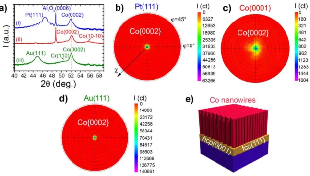
In contrast to electron microscope techniques that give information on limited sample areas, X-Ray diffraction (XRD) allows interrogating the sample over large areas. Therefore, it was the method of choice for the crystallographic characterization of the obtained nanostructured films. The symmetric diffractograms (Fig. 3a) indicate that the Co(0002) planes are parallel to the Pt(111), Co(0001) and Au(111) planes, respectively (the different axes and angles relevant to the XRD measurements are shown in Figure S3). Combined to the TEM observations, these data show that the wires grow vertically along the Co[0002] direction whatever the metallic film of 6-fold symmetry. In order to precise the NW spatial orientation, we performed XRD texture measurements to record the pole figure of the Co{0002} reflections, i.e. the NW growing planes (Figure 3b-d, and Methods section). Indeed, as NWs grow along the (0001) planes in a single-crystal hcp structure, the spatial orientation of the (0001) planes corresponds to the NW ones. The Co{0002} pole figures recorded on NW arrays grown on 6-fold symmetry surfaces reveal that the Co[0002] growth direction, and consequently the direction of the NW long axis, is narrowly distributed around the substrate out-of-plane direction (==0°), even if a larger distribution is recorder for Co NWs/Co(0001). A 3D scheme of the vertical NWs grown on 6-fold symmetry surfaces is given in Figure 3e.
11
All the above mentioned data indicate that the Co(0001) crystalline orientation and therefore the vertical growth of Co cylindrical nanocrystals are governed by the symmetry matching between the Co(0001) growing plane and the different 6-fold symmetry surfaces, whatever the associated lattice mismatches with Co (Co/Pt = -9.5%, Co/Co = 0, Co/Au = -13.1%). This is consistent with the hexagonal close-packed (hcp) Co(0001) growth orientation reported in thin film growth studies of Co/Pt(111)42,43 and Co/Au(111)44,45 by physical vapor deposition techniques.
Figure 3. (a) XRD 2 diffractograms (Co Kα1) of Co NW arrays grown on different metallic films:
(i) Pt(111), (ii) Co(0001), and (iii) Au(111) (Co/LA/HDA ratio: 1/2/2, [Co] = 5mM, 24h, 150°C, solvent: anisole). The diffractogram measured on Co NWs/Au(111) also presents the Si(004) peak of the substrate at 2=82.42° (not shown). Pole figures of the Co{0002} reflections (2=51.47°) measured on (b) Co NWs/Pt(111), (c) Co NWs/Co(0001), and (d) Co NWs/Au(111). (e) Schematic representation of a Co NW array on 6-fold symmetry surfaces.
12
In terms of magnetic properties, magnetic measurements reveal that NW arrays on 6-fold symmetry surfaces exhibit hysteresis loops characteristic of ferromagnetic materials at room temperature. On Pt(111), Co NWs/NRs present a magnetic anisotropy perpendicular to the substrate: the hysteresis loops are more square with higher remnant magnetizations and coercive fields when the magnetic field is applied perpendicular to the metallic film, i.e. parallel to the NRs/NWs (Supporting Fig. S4). This behavior results from the intrinsic shape anisotropy of the NWs/NRs, combined with the uniaxial magnetocrystalline anisotropy along the Co[0001] direction, and this despite important dipolar interactions.39 The association of a high
magnetocrystalline anisotropy and a high density is a pre-requisite for application in magnetic recording, therefore the hcp single-crystalline structure is highly desirable for this application. On Co(0001), despite the similar overall structure to the Pt(111) which presents an out-of-plane easy axis of the NR array, only a weak magnetic anisotropy is measured along the substrate plane (Supporting Fig. S5). This is attributed to the in-plane contribution of the 20 nm thick Co(0001) film on which NRs have grown. An important point concerns the absence of Co/Co oxide exchange bias in the low temperature hysteresis loops of the Co NWs/Pt(111) samples preserved from air-exposure during transfer to the magnetometer (Supporting Fig. S4b). This demonstrates that, as in the case of the synthesis of Co nanorods and nanowires in homogeneous conditions, i.e. without substrates,40,41 the Co NW growth process intrinsically provides oxygen
free Co nano-objects. If samples are air-exposed, a Co/Co oxide exchange bias is measured at low temperature and the saturation magnetization slightly decreases. We believe the CoO surface layer passivates the nanowires that retain their metallic core even after long air exposure as confirmed by checking by magnetic measurements at various time intervals (Supporting Fig. S6).
13
Co nanowire growth on 4-fold symmetry metallic films
The same Co growth conditions in the presence of crystalline surfaces of 4-fold symmetry
results in different orientations of nanostructures, the growth direction of which are dictated by the substrate.
Co decomposition on Pt(001)
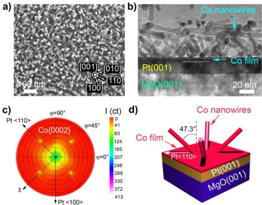
Figure 4 displays the NR array obtained on a Pt(001) film after a 3 days reaction at 100°C and
with a Co/LA/HDA ratio of 1/1.2/1.2. The SEM micrograph of Figure 4a shows tilted NRs with in-plane projections of the NR directions along the Pt<110> directions of the Pt(001) film. The TEM cross-section indicates that an intermediate Co layer of around 5 nm is present between the Pt(001) film and a layer of slanted NRs (Figure 4b). The NRs have diameters around 8 nm and grow along the hcp Co[0001] axis. Texture measurements by XRD were carried out in order to identify the Co NR orientations. The resulting pole figure of the Co{0002} reflections shown in Figure 4c reveals 4 satellite spots at =45, 135, 225 and 315° indicating that the NRs are oriented along 4 distinct directions and form an angle of =47.3° with the normal of the film, i.e. the Pt[001] axis (precise angle measurements are shown in Supporting Fig. S7). The large spot measured in the central area of the pole figure (at ==0°) could be due to parasite diffraction of the MgO(002) and Pt(002) planes, as MgO(002) and Pt(002) diffract at angles close to the Co(0002) one, and no Co(0002) peak appears in the XRD 2 diffractogram (Supporting Fig. S8). However, the presence of a limited number of vertical Co NRs on Pt(001) cannot be totally ruled out. The Co{0002} pole figure also indicates that the in-plane projections of the tilted NRs are aligned along the Pt<110> directions. From the analysis developed above, the NR orientations on Pt(001) are summarized in Figure 4d. A reaction under conditions corresponding to a nanowire synthesis (Co/LA/HDA ratio of 1/2/2) was also performed on Pt(001) and also
14
leads to tilted NWs with identical spatial orientations to the ones described for NRs (Supporting Fig. S9).
Figure 4. (a) SEM micrograph of a Co NR array grown on Pt(001)/MgO(001) (Co/LA/HDA ratio: 1/1.2/1.2, [Co] = 2.1mM, 3.5 days, 100°C, solvent: toluene) Inset: crystalline directions of the Pt(001) film. (b) Cross-sectional TEM micrograph of the same sample. (c) XRD pole figure of the Co{0002} reflections, indicating 4 satellite spots at =47.3°. (d) Schematic 3D view of the Co NR orientations on Pt(001).
While rationalisation of the growth orientation of Co NRs/NWs on Pt(001) films is not straightforward, an explanation can be given considering the presence of a 5 nm intermediate Co layer on Pt(001), in association to the measured tilt angle of the NRs/NWs. We assume that during the first stages of the growth, Co island nucleation occurs on Pt to form the intermediate
15
Co layer. From the measured tilt angle of the NWs, it is proposed that Co hcp nuclei grow on Pt(001) along Co(11-23) planes as opposed to the growth along Co(0001) planes on 6-fold symmetry metallic films. Upon growth, these Co(11-23) islands should exhibit facets composed of (0001) planes in order to minimize their surface energy because such planes are the ones of minimum energy in bulk hcp Co.46 Since (0001) and (11-23) planes form an angle of 47.26° in
bulk hcp Co, the (0001) facets of the islands are oriented at 47.26° from the substrate plane (Supporting Figure S10). As already shown, deposition of Co from the solution on Co(0001) planes induces a vertical NW growth (Figures 1b, 2d, 3c). Therefore Co deposition on (0001) facets of Co(11-23) islands results in NW growth perpendicularly to (0001) facets, i.e. along directions at 47.3° from the normal of the substrate plane, as measured experimentally. In this description, the Co(11-23) islands would compose the observed 5 nm thick layer on Pt(001). Despite the fact that the Co(11-23) growth orientation on Pt(001) has never been reported before, whatever the deposition technique, such (11-23) planes would reduce the lattice parameter misfits between Co and Pt lattices (Supporting Fig. S11).
In terms of magnetic properties, the peculiar Co NRs/NWs orientations on Pt(001) induce strong differences in comparison to vertical Co NRs/NWs on 6-fold symmetry surfaces. As the anisotropy is high along the NW long axis due to the uniaxial Co hcp magnetocrystalline anisotropy, the different NR/NW directions for NRs/NWs grown on Pt(001) induce a dispersion of the magnetic easy axes. Moreover, the 5nm Co intermediate layer is expected to favor an in-plane anisotropy. Consequently, the out-of-in-plane direction is a hard axis and a weak anisotropy is observed along the substrate plane (Supporting Fig. S12). Qualitatively, micromagnetic simulations illustrate the influence of the NR orientation distribution and of the Co intermediate layer on the magnetic behavior (Supporting Fig. S13).
16
Co decomposition on Cu(001)
A different NW configuration is obtained by using a Cu(001) film as a 2D seed. After a
reaction with a Co/LA/HDA ratio of 1/2/2 during 24h at 150°C, the SEM and TEM cross-section micrographs also show tilted nanowires on the whole substrate surface (Figure 5a,b respectively). The NW diameter is estimated by TEM to be around 11 nm. TEM observations allow distinguishing two different growth directions (see dashed lines on Figure 5b). As seen in Figure 5c, the Co{0002} pole figure is composed of 8 satellite spots, 4 at =54.3° and 4 at =15.5° (precise angle measurements in Supporting Fig. S14a-b). As summarized on the 3D scheme given in Figure 5d, it is concluded that there exist 8 directions of tilted NWs, 4 forming an angle of about 15.5° with the normal of the substrate (i.e. the Cu[001] axis) and 4 forming an angle of about 54.3°. These 8 directions have projections on the substrate plane that are aligned along the Cu<110> directions.
17
The origin of the tilted NW orientations on Cu(001) can be rationalized as in the Co NWs/Pt(001) system. Based on the measured tilt angles, it is suggested that the Co nucleation on the Cu(001) film induces the growth of face-centered cubic (fcc) Co islands of Co(001) and Co(221) orientations (i.e. islands with Co(001) and Co(221) planes parallel to Cu(001), respectively). The fcc Co(001) growth orientation is commonly reported in Co ultra-thin films deposited on Cu(001) surfaces by physical vapour deposition techniques.47-49 Furthermore, the
Figure 5. (a) SEM micrograph of a Co NW array grown on Cu(001)/MgO(001) (Co/LA/HDA ratio: 1/2/2, [Co] = 5mM, 24h, 150°C, solvent: anisole). (b) Cross-sectional TEM micrographs of the same sample (the dashed lines indicate the two tilted growth directions). (c) XRD pole figure of the Co{0002} reflections, indicating 4 satellite spots at =15.5° and 4 at =54.3°. (d) Schematic 3D view of the Co NW orientations on a Cu(001) film.
18
growth of fcc Co(001) on Cu(001) is confirmed by XRD measurements (Supporting Fig. S14d). We believe that fcc Co(001) islands expose facets composed of Co(111) planes, that is, planes forming an angle of 54.74° with respect to Co(001) planes in bulk fcc Co. Since a fcc Co(111) plane is identical to a hcp Co(0001) plane in terms of symmetry and interatomic distances, a deposition of Co from the solution on these planes would result to the anisotropic growth of Co and consequently to Co NWs tilted at an averaged measured angle of 54.3° from the normal of the substrate (see fcc Co(001) island description in Supporting Fig. S15a). Following the same reasoning, fcc Co(221) islands could nucleate on Cu(001) and exhibit facets composed of (111) planes which form an angle of 15.79° with the (221) planes in bulk fcc Co. Such facets could induce a Co[0001] growth and therefore the resulting NW long axis at defined directions from the normal of the substrate plane, that is, at 15.5° as measured experimentally (see fcc Co(221) island description in Supporting Fig. S15b). To the best of our knowledge, the growth of fcc Co(221) has never been reported in Co ultra-thin films deposited on Cu(001) surfaces, whatever the deposition techniques. Nevertheless, it can be shown that the lattice parameter mismatch between fcc Co(221) and Cu(001) is the same as between fcc Co(001) and Cu(001) (Supporting Fig. S16). A third NW orientation on Cu(001) can be deduced from the XRD Co{0002} pole figure in Figure 5c. The intense central spot at ==0° could be attributed to vertical NWs because the XRD -2 diffractogram (Supporting Fig. S14d) clearly shows a hcp Co(0002) peak (or fcc Co(111) as they diffract at the same angle) which indicates that Co planes of 6-fold symmetry are parallel to the substrate. These NWs may result from Co islands of either hcp Co(0001) or fcc Co(111) growth orientation which are also present on Cu(001), however without an epitaxial relationship with Cu(001) due to symmetry mismatch. Such islands could then induce a vertical growth of Co NWs. The presence of parasitic Pt(111) crystallites in the Pt
19
buffer layer introduced to enhance the crystalline orientation of the Cu film can moreover favor such a hcp Co(0001) or fcc Co(111) growth orientation (Fig. S14d). Contrary to the case of Co NW/Pt(001), the presence of a Co intermediate layer at the Co NW/Cu(001) interface has not been clearly detected by TEM. However, it has to be noted that the Co/Cu interface area is ill defined with disturbed contrasts in TEM, presumably due to a preferential Cu etching during the cross-sectional sample preparation.
Finally, the growth of Co nanowires has been attempted on commercial thin Cu foils instead of orientated crystalline films. The results show that the Co NW growth is effective on 50µm thick Cu foils, with tilted and vertical NWs in less well-defined orientations than for the previous cases due to the polycristallinity of the substrate (Supporting Fig. S17). Such behaviour is consistent with the above mentioned results demonstrating the peculiar link between the NW growth orientations and the crystallographic orientation of the metallic film. The table 1 summarizes the characteristics of the Co NW growth on different substrates.
6-fold symmetry surfaces 4-fold symmetry surfaces Polycrystalline textured surface Pt(111) Co(0001) Au(111) Pt(001) Cu(001) Cu
NW
orientation vertical vertical vertical tilted (47.3°)
tilted
(15.5° and 54.3°)
vertical and tilted (15° and 54°) NW diameter
(nm) 6 8 9 8 11 -
NW length
(nm) 1080 1000 1300 - 700 -
Table 1. Characteristics of the Co NWs grown on different substrates after a similar chemical
20
Fe decomposition on Pt(001) and Pt(111)
In order to demonstrate the large scope of the solution epitaxial growth method, the same strategy has been applied for the growth of Fe nanostructures. We previously demonstrated that the reduction by H2 of [Fe{N(SiMe3)2}2] in solution in the presence of long chain amine and
long-chain acid ligands leads to Fe nanocubes and nanostars.50 Under similar experimental
conditions and in the presence of Pt(111) and Pt(001) surfaces, Fe nanostructures were successfully grown and present patterns which depend on the Pt crystallographic orientation as shown in Figure 6. After 24h reaction, the Fe nanostructures on Pt(001) consist in cubic-like structures (Fig. 6b). On the other hand, the Fe structures on Pt(111) can be viewed as triangular prisms, i.e. elongated and truncated cubes along {110} planes (Fig. 6a). The same characteristic surface features persist after several days of reaction (Supporting Fig. S18). Transmission Electron Microscopy (TEM) of a cross-section for both samples after 3 days of reaction evidence thick body-centered cubic (bcc) Fe columnar films above the Pt layer of around 80 nm for Pt(111) (Fig.6c) and 40 nm for Pt(001) (Fig. 6d), suggesting the merging of the nanostructures towards a Fe film. The XRD diffractograms show that Fe grows mainly along bcc Fe(110) on Pt(111) (Fig. 6e) and along bcc Fe(001) on Pt(001) (Fig. 6f), as observed in thin films elaborated by classical vapour-phase methods.51,52 The epitaxial growth of Fe on both substrates
is illustrated by -scan diagrams on Fe reflections (insets in Fig. 6e, f). Detailed information on the structure and the epitaxial relationships are given in Supporting Fig. S19. Thus, the decomposition of Fe in the presence of either Pt(001) or Pt(111) surfaces leads to nanostructured epitaxial films of metallic bcc Fe, the growth direction being dictated by the Pt exposed surface. The schematic views of Fig. 6g and h illustrate the overall feature of Fe nanostructure orientations obtained on Pt(001) and Pt(111) surfaces respectively. As expected, the Fe layers
21
obtained after 3 days of reaction are ferromagnetic at room temperature with an in-plane easy axis of magnetization (Supporting Fig. S20).
Figure 6. SEM micrographs of Fe nanostructures grown on (a) Pt(111) and (b) Pt(001) films, respectively (Fe/LA/HDA: 1/2/1, [Fe]=2.5mM, 24h, 150°C, solvent: anisole). (c), (d): TEM cross-section micrographs of the Fe/Pt(111) and the Fe/Pt(001) growths, respectively (3 days reaction). (e), (f): XRD diffractograms and -scan in inset (3 days reaction). (g), (h): Schematic 3D views of the Fe nanostructure orientations obtained on Pt(111) and Pt(001) films respectively before coalescence takes place.
22
DISCUSSION
We have demonstrated that the reduction of a metal complex in solution under mild conditions allows the growth of Fe and Co nanostructures on crystalline metallic films. The growth is epitaxial in both cases and the nanostructure orientations are dictated by the crystalline orientation of the film. Concerning Co, on 6-fold symmetry films, we observed a common vertical NR/NW orientation independently of the lattice mismatch. On the other hand, 4-fold symmetry films induce nanowire growth along different orientations. Thus, in all cases the growth process ends-up by forming NRs/NWs similar to those obtained in the absence of any substrate,40,41 and this irrespectively of the film characteristics. Concerning Fe, the obtained
nanostructures on Pt surfaces can be viewed as merged cubic nanoparticles, truncated along different directions, and with distinct orientations, which depend on the symmetry of the metallic film.
These results allow proposing a general growth mechanism. Before reduction takes place, the metal reservoir consists of several species of different reactivity due to the reaction of the metallic precursor with the amine and acid ligands.40,41 The most unstable species are the first to
be reduced supplying the first metallic atoms. This first step of heterogeneous nucleation on the film surface leads to nuclei with a crystalline orientation dictated by the symmetry of the surface. As the reaction proceeds, atoms coming from the more stable metal species in solution start to be reduced and add to the nuclei which start to grow. In parallel, upon decomposition of the molecular metallic species, the liberated organic ligands define the size and shape of the islands formed on the surface, by preferential coordination on their less stable facets.
In the case of the formation of free Co NRs, this effect inhibits Co deposition on (10-10) planes which constitutes the wire lateral planes while favoring Co growth along (0001) ones
23
which give rise to an anisotropic growth along the Co[0001] direction. Indeed, free Co nanorods grow along their long axis, that is, by Co addition to Co(0001) facets,32,33,40 whereas in the case
of multipods, nanowires of hcp structure grow from Co(111) facets of fcc seeds.41 The present
results demonstrate that the same shape-directing function of the organic ligands also acts in the presence of the substrate and consequently leads to an assembly of NWs on the substrate as opposed to a Co film. We suggest that the crystalline orientation of Co nuclei on 6-fold symmetry surfaces is hcp with Co(0001) growing planes irrespective of the respective lattice parameter mismatches. On 4-fold symmetry surfaces, it is assumed that fcc or hcp Co islands can be stabilized depending on their mismatch with Cu(001) or Pt(001) metallic surfaces. Indeed, the appearance of the different growth orientations, i.e. fcc Co(001) and (221) on Cu(001) and hcp Co(11-23) on Pt(001), could be rationalized in terms of minimized lattice parameter mismatch (Supporting Table S2). It is postulated that the anisotropic Co growth occurs on the 6-fold symmetry facets presented by both hcp and fcc Co islands, that is, on Co(111) facets of fcc Co islands or Co(0001) facets of hcp ones. This step would require a certain island size and consequently could lead to an intermediate layer of coalesced islands between the NWs and the metallic film before NRs/NWs start to appear, as for Co NWs/Pt(001). Once the anisotropic growth is engaged on specific facets, it is pursued on Co(0001) planes, and adopting the shape imposed by the solution.
In this description, the Fe nucleation on metallic surfaces also leads to nuclei with crystallographic orientations dictated by the surface. In the absence of a substrate, the growth of Fe nanocrystals in solution leads to bcc Fe cubes or concave cubes with ligands acting as shape-directing agents.50 In the presence of a substrate, we postulate that the ligands play the same
24
symmetry implies a Fe <100> preferential growth direction which is not a strictly anisotropic growth direction as opposed to Co NR/NW. As both Fe(110) and Fe(100) orientations obtained on Pt(111) and Pt(001) respectively possess a <100> direction along the film plane (Fig. 6g,h), the Fe initial nanostructures on Pt grow also along the substrate plane. Consequently, as the reaction proceeds, the Fe nanostructures continue to grow on Pt and finally merge together to give a nanostructured film.
Despite the fact that several points remain unclear for the moment (differences in NR/NW diameters, different Fe film thickness at long reaction time), our results suggest that the solution finally imposes its natural tendency by (i) allowing a pre-structuration of the substrate film by epitaxial nucleation of islands and (ii) selecting island facets from which the growth can take place as dictated by its composition. This is the key point of the present results suggesting that the growth of shape-controlled nanocrystals, well-controlled in solution phase syntheses, can operate on appropriate 2D seeds and proceed via self-organization of the nano-objects on a planar device. This concept is of fundamental interest because it means that the different nanocrystals reported in the literature and synthesized by wet chemical methods could in principle be grown on suitable films. In the case of anisotropic nanocrystals, such as Co NRs/NWs, this approach is particularly attractive, illustrating the efficient coupling between the intrinsic Co anisotropic crystal lattice and specific organic ligand coordination leading to different growth possibilities, tilted or not, depending on the substrate used. Extension of the method to other anisotropic nanocrystals synthesized by solution phase syntheses will open interesting new bottom-up approaches for nanotechnology.
25
CONCLUSION
Here we report the detailed general approach of a solution phase synthesis of purely metallic nano-objects on various metallic surfaces of different crystalline symmetries. The most interesting system, which benefits from the Co intrinsic anisotropic growth, concerns the Co NRs/NWs growth on surfaces by decomposition of a Co coordination precursor in the presence of acid and amine ligands. Indeed, the use of 6-fold symmetry substrates of various metals yields Co NWs grown perpendicularly to the substrate surface, without any exception. On the other hand, 4-fold symmetry substrates give rise to nanowires that grow at well-defined, albeit different orientations depending on the epitaxial relationships and the lattice mismatch between the substrate and the nucleating Co islands. The case of Fe confirms the generality of the approach and shows that as expected, if the nanocrystal growth is not strictly anisotropic, the obtained nanostructures tend to merge together upon growth, at longer reaction times, to result in a nanostructured film instead of an array of distinct nano-objects.
These results have no precedent using physical deposition methods. We previously presented the interesting magnetic properties of ultra-dense arrays of NWs on Pt(111), particularly interesting in the field of future magnetic recording where the high dipolar interactions experienced at ultra-high densities can be overcome thanks to the uniaxial magnetocrystalline anisotropy of the single-crystalline hcp NWs to result in a perpendicular magnetic anisotropy.39
On the other hand, the growth of tilted NWs on 4-fold symmetry metallic films represents an original approach to support non-aggregated 1D catalysts on a substrate. The use of fully conductive, ductile and inexpensive substrates such as thin Cu foil is particularly attractive. In addition, considering the larger scope of metallic 1D nanocrystals, by adapting the solution syntheses of free metallic NWs reported in the literature to induce their heterogeneous nucleation
26
and growth on a substrate, the solution epitaxial growth method could constitute an alternative to the VLS method for the growth of metallic NWs on surfaces. Finally, thanks to the ability of chemical approaches to induce the epitaxial growth of various materials on pre-synthesized nanocrystals,36 one can envisage to modify the nanowires of an array through subsequent
deposition steps of other materials towards more complex nanostructures and multifunctional materials of specific properties.
METHODS
Thin film fabrication. The crystalline metallic films were grown in a vacuum chamber
(3×10⁻⁸ mbar) connected to a glove box in order to avoid any oxygen or water contamination
when passing from physical vapour deposition to chemical solution growth. Before film deposition, the 10mm×10mm×1mm α-Al2O3(0001) sapphire and Mg0(001) substrates (furnished
by Neyco) were annealed at 750 °C for an hour under high vacuum, in order to clean the surface. The 20nm thick films were deposited using thermal evaporation or Direct Current (DC) magnetron targets at 5×10⁻³ mbar Ar pressure. Details about the deposition conditions of the
different epitaxial films are listed in the Supporting Table 1 (temperature, buffer layer, etc). X-ray diffraction (XRD) and X-X-ray reflectivity (XRR) measurements were performed in order to control the growth orientation and epitaxy, the thickness and the roughness degree. The 10mm×10mm×50µm commercial Cu foils were purchased from Neyco. They were conditioned in individual oxygen-free sachets and kept in the glove-box. They were opened immediately prior to use and immersed in the growth solution without any further treatment.
Co nanowire growth. All solutions were prepared in a glove-box, toluene was distilled,
27
sieves (Acros-Organics 4A 8-12 Mesh) to remove traces of water. Anhydrous anisole was purchased from Aldrich (99,7%) and kept in the glove-box under activated molecular sieves in order to remove traces of water. The metal precursor [Co{N(SiMe3)2}2(thf)] was furnished by
NanoMePS. Hexadecylamine (HDA) (Aldrich) and lauric acid (LA) (Acros) were kept in the glove box and used as received.
In a representative reaction resulting in the growth of long nanowires, a solution of [Co{N(SiMe3)3}2 (thf)] (22.6 mg, 0.05 mmol), in 2 ml of anisole is rapidly added to a mixture of
HDA (24.2 mg, 0.10 mmol) and LA(20.0 mg, 0.10 mmol) in 8 ml of anisole (Co/LA/HDA molecular ratio = 1/2/2, [Co] = 5mM). The solution is introduced in a Fischer-Porter pressure bottle. The substrate is immersed in the solution with the metallic film facing the bottom of the bottle. The Fischer-Porter is removed from the glove-box, the Ar is evacuated and the bottle is charged with H2 to 3 bars. The solution containing the substrate is heated to 150°C for 24h. At
the end of the reaction the solution is cooled down and the Fischer-Porter transferred to the glove box. A TEM grid is prepared by drop-casting some drops of the supernatant solution. At the end of the reaction, the solution is cooled down with cold water and transferred into the glove box. The substrate is removed from the solution and washed 3 times with toluene, then washed twice with a solution of HDA in THF (tetrahydofurane) (10 mg/mL), assisted by ultra sounds during 1 minute, and finally washed in toluene. The substrate was then observed by SEM. The same procedure is used in all experiments.
The same procedure is followed for the formation of nanorods, by adjusting the amounts of reactants so that Co/LA/HDA = 1/1.2/1.2. and [Co] = 2.1mM, and by performing the reaction at 100°C for longer reaction times. Toluene was used instead of anisole for the reactions performed at 100°C, unless otherwise stated. The specific reaction conditions (concentrations, temperature,
28
reaction times) for each case are mentioned in the text and/or in the corresponding Figure captions.
Iron growth. A solution of [Fe{N(SiMe3)2}2] (9.4 mg, 0.012 mmol), in 2 ml of anisole is rapidly
added to a mixture of HDA (6.0 mg, 0.025 mmol) and LA (10.0 mg, 0.050 mmol) in 8 ml of anisole (Fe/LA/HDA = 1/2/1, [Fe] = 2,5mM). The solution is introduced in a Fischer-Porter pressure bottle. The substrate is then immersed in the solution with the Pt layer facing the bottom of the bottle. The Fischer-Porter is removed from the glove-box and charged with H2 to 3bars
during 7 min. The reaction is heated to 150°C for 24h or 3 or 4 days. At the end of the reaction the solution is cooled down and the Fischer-Porter transferred to the glove box. The substrate is washed with toluene in order to remove the organic surfactants and observed by FEG-SEM. A TEM grid is prepared by drop-casting some drops of the transparent supernatant solution in order to verify whether homogeneous growth has taken place in solution.
Electron microscopy (SEM and TEM). The FEG-SEM (Field Emission Gun-Scanning
Electron Microscopy) observations were carried out on a JEOL JSM6700F. Samples for cross-sectional TEM analysis were prepared following the standard method: the samples were first mechanically polished down to about 10 micron thickness, then the final thinning to electron transparency was achieved by ion milling at low angle (7°) and low voltage (5 kV) using a Precision Ion Polishing System (PIPS from Gatan). The TEM samples were investigated using a Tecnai F20 fitted with a Cs corrector (CEOS) which point resolution is 0.12 nm.
X-ray Diffraction (XRD). The X-ray diffraction measurements were performed on a θ-2θ
29
select Co Kα1 radiation (λKα1Co = 1.78901 Å). The different axes of the diffractometer are
displayed on Supporting Figure S3. Each pole figure is recorded during approximately 60h.
Supporting Information Available: Details about thin film fabrication, definition of the angle
during X-ray diffraction experiments, TEM micrograph of Co NWs/Au(111), SEM micrographs of Co NRs/Pt(111) and Co NRs/Co(0001), complementary XRD datas of Co NWs/Pt(001) and Co NWs/Cu(001), schematic illustrations of hcp Co(11-23) islands on Pt(001), fcc Co(221) islands on Cu(001) and fcc Co(001) islands on Cu(001), lattice parameter mismatches between fcc Co(001), fcc Co(221), hcp Co(11-23) and Cu(001) and Pt(001) films respectively, SEM and XRD data of Co NWs grown on Cu foils, SEM micrographs of Fe nanostructures on Pt(111) and Pt(001) films after long reaction times, two-dimensional surface lattice configurations of Fe on Pt(001) and Pt(111), magnetic hysteresis loops of Co NRs/Pt(111), Co NWs/Pt(111), Co NRs/Co(0001), Co NRs/Pt(001) and Fe nanostructured films on Pt(111) and Pt(001). This material is available free of charge via the Internet at http://pubs.acs.org.
AUTHOR INFORMATION
Corresponding Author
*Blon Thomas, [email protected] * Katerina Soulantica, [email protected]
Present Addresses
† Nikos Liakakos, [email protected], +1-510-486-4251, Chemical Sciences Division, Lawrence Berkeley National Laboratory, 1 Cyclotron Road, Berkeley, California 94720, United States. †† Benoit Cormary, [email protected], +33 5 61 33 31 39, CNRS, LCC (Laboratoire de Chimie de Coordination), 205 route de Narbonne, 31077 Toulouse Cedex 4, Université de Toulouse, UPS, INPT, 31077, Toulouse, France.
30
Conflict of Interest: The authors declare no competing financial interest.
ACKNOWLEDGMENTS
The authors thank the ANR for the BATMAG project (ANR-07-BLAN-0296), the DENSAR project (ANR-14-CE07-0025-01), the European Commission for the FP7 NAMDIATREAM project (EU NMP4-LA-2010-246479), the European Commission and the Région Midi-Pyrénées for the POCTEFA Interreg project (MET-NANO EFA 17/08), the European Commission, FEDER and the Région Midi-Pyrénées for NANOBAT I and II projects and the TEMSCAN service for the SEM.
ABBREVIATIONS
VLS vapor-liquid-solid ; NRs nanorods ; NWs nanowires ; LA lauric acid ; HDA hexadecylamine ; SEM scanning electron microscope; TEM transmission electron microscopy ; XRD X-ray diffraction ; CVD chemical vapor deposition ; hcp hexagonal close-packed ; fcc face-centered cubic ; bcc body-centered cubic.
REFERENCES
1 Gao, Y.; Tang, Z. Design and Application of Inorganic Nanoparticle Superstructures: Current
Status and Future Challenges. Small 2011, 7, 2133-2146
2 Grzelczak, M.; Vermant, J.; Furst, E. M.; Liz-Marzan, L. M. Directed Self-Assembly of
31
3 Chen, Q.; Chul Bae, S.; Granick, S. Directed Self-Assembly of a Colloidal Kagome Lattice.
Nature 2011, 469, 381-384
4 Vigderman, L.; Khanal, B. P.; Zubarev, E. R. Functional Gold Nanorods: Synthesis,
Self-Assembly, and Sensing Applications. Adv. Mater. 2012, 24, 4811–4841
5 Li, L.; Seng, K. H.; Chen, Z.; Guo,Z.; Liu, H. K. Self-Assembly of Hierarchical Star-like
Co3O4 Micro/Nanostructures and their Application in Lithium Ion Batteries. Nanoscale 2013, 5, 1922-1928
6 Whitesides, G. M.; Grzybowski, B. Self-Assembly at all Scales. Science 2002, 295, 2418-2421 7 Busseron, E.; Ruff, Y.; Moulin, E.; Giuseppone, N. Supramolecular Self-Assemblies as
Functional Nanomaterials. Nanoscale 2013, 5, 7098-7140
8 Kwiat, M.; Cohen, S.; Pevzner, A.; Patolsky, F. Large-Scale Ordered 1D-Nanomaterials
Arrays: assembly or not ? Nano Today 2013, 8, 677-694
9 Nie, Z.; Petukhova, A.; Kumacheva, E. Properties and Amerging Applications of
Self-Assembled Structures Made from Inorganic Nanoparticles. Nat. Nanotechnol. 2010, 5, 15-25
10 Amatore, C. Is there an Intrinsic Limit to the Size of 2D Supracrystals Built from Weakly
Interacting Nanoparticles ? Chem. - Eur. J. 2008, 14, 8615-8623
11 Greene, L. E.; Yuhas, B. D.; Law, M.; Zitoun, D.; Yang, P. Solution-Grown Zinc Oxide
32
12 Wagner, R. S.; Ellis, W. C. Vapor‐Liquid‐Solid Mechanism of Single Crystal Growth. Appl.
Phys. Lett. 1964, 4, 89-90
13 Wang, N.; Cai, Y.; Zhang, R. Q. Growth of Nanowires. Mater. Sci. Eng., R 2008, 60, 1-51 14 Adhikari, H.; Marshall, A. F.; Chidsey, C. E. D.; McIntyre, P. C. Germanium Nanowire
Epitaxy: Shape and Orientation Control. Nano Lett. 2006, 6, 318-323
15 Lugstein, A.; Steinmair, M.; Hyun, Y. J.; Hauer, G.; Pongratz, P.; Bertagnolli, E.
Pressure-Induced Orientation Control of the Growth of Epitaxial Silicon Nanowires. Nano Lett. 2008, 8, 2310-2314
16 Vayssieres, L. An Aqueous Solution Approach to Advanced Metal Oxide Arrays on
Substrates. Appl. Phys. A: Mater. Sci. Process. 2007, 89, 1-8
17 Appell, D. Wired for Success. Nature 2002, 419, 553-555
18 Martin, C. R. Nanomaterials: a Membrane-Based Synthetic Approach. Science 1994, 266,
1961-1966
19 Lee, W.; Park, S.-J. Porous Anodic Aluminum Oxide: Anodization and Templated Synthesis
of Functional Nanostructures. Chem. Rev. 2014, 114, 7487-7556
20 Thurn-Albrecht, T. ; Schotter, J.; Kästle, G. A.; Emley, N.; Shibauchi, T.; Krusin-Elbaum, L.;
Guarini, K.; Black, C. T.; Tuominen, M. T.; Russell, T. P. Ultrahigh-Density Nanowire Arrays Grown in Self-Assembled Diblock Copolymer Templates. Science 2000, 290, 2126-2129
33
21 Brumlik, C. J.; Menon, V. P.; Martin, C. R. Template Synthesis of Metal Microtubule
Ensembles Utilizing Chemical, Electrochemical, and Vacuum Deposition Techniques. J. Mater. Res. 1994, 9, 1174-1183
22 Huczko, A. Template-Based Synthesis of Nanomaterials. Appl. Phys. A: Mater. Sci. Process.
2000, 70, 365-376
23 Zhang, X. Y.; Xu, L. H.; Dai, J. Y.; Chan, H. L. W. Fabrication and Magnetic Behavior of Co–
Ni Nanowire Arrays with Small Diameters. Phys. B (Amsterdam, Neth.) 2004, 353, 187-191
24 Darques, M.; Encinas, A.; Vila, L.; Piraux, L. Controlled Changes in the Microstructure and
Magnetic Anisotropy in Arrays of Electrodeposited Co Nanowires Induced by the Solution pH. J. Phys. D: Appl. Phys. 2004, 37, 1411–1416
25 Vidal, F. ; Zheng, Y. ; Schio, P.; Bonilla, F. J. ; Barturen, M. ; Milano, J. ; Demaille, D. ;
Fonda, E. ; de Oliveira, A. J. A. ; Etgens, V. H. Mechanism of Localization of the Magnetization Reversal in 3 nm Wide Co Nanowires. Phys. Rev. Lett. 2012, 109, 117205
26 Jamet, M.; Barski, A.; Devillers, T.; Poydenoet, V. ; Dujardin, R. ; Bayle-Guillemaud, P. ;
Rothman, J. ; Bellet-Amalric, E.; Marty, A.; Cibert, J.; et al. High-Curie-Temperature Ferromagnetism in Self-Organized Ge1−xMnx Nanocolumns. Nat. Mater. 2006, 5, 653-659
27 Mohaddes-Ardabili, L.; Zheng, H.; Ogale, S. B. ; Hannoyer, B.; Tian, W.; Wang, J.; Lofland,
S. E.; Shinde, S. R.; Zhao, T.; Jia, Y.; et al. Self-Assembled Single-Crystal Ferromagnetic Iron Nanowires Formed by Decomposition. Nat. Mater. 2004, 3, 533-538
34
28 Kim, S-I.; Yoon, H.; Lee, H.; Lee, S.; Jo, Y.; Lee, S.; Choo, J.; Kim, B. Epitaxy-Driven
Vertical Growth of Single-Crystalline Cobalt Nanowire Arrays by Chemical Vapor Deposition. J. Mater. Chem. C 2015, 3, 100-106
29 Yao, J.; Liu, Z.; Liu, Y.; Wang, Y.; Sun, C.; Bartal, G.; Stacy, A. M.; Zhang, X. Optical
Negative Refraction in Bulk Metamaterials of Nanowires. Science 2008, 321, 930
30 Liu, Q.; Cui, Y.; Gardner, D. ; Li, X. ; He, S.; Smalyukh, I. I. Self-Alignment of Plasmonic
Gold Nanorods in Reconfigurable Anisotropic Fluids for Tunable Bulk Metamaterial Applications. Nano Lett. 2010, 10, 1347–1353
31 Terris, B. D.; Thomson, T. Nanofabricated and Self-Assembled Magnetic Structures as Data
Storage Media. J. Phys. D: App. Phys. 2005, 38, R199-R222
32 Dumestre, F.; Chaudret, B.; Amiens, C.; Respaud, M.; Fejes, P. Unprecedented Crystalline
Super-Lattices of Monodisperse Cobalt Nanorods. Angew. Chem., Int. Ed. 2003, 42, 5213 –5216
33 Dumestre, F.; Chaudret, B.; Amiens, C.; Fromen, M-C.; Casanove, M-J.; Renaud, P.; Zurcher,
P. Shape Control of Thermodynamically Stable Cobalt Nanorods Through Organometallic Chemistry. Angew. Chem., Int. Ed. 2002, 41, 4286-4289
34 Heng, H.; Gibbons, P. C.; Kelton, K.F.; Buhro, W. E. Heterogeneous Seeded Growth: A
Potentially General Synthesis of Monodisperse Metallic Nanoparticles. J. Am. Chem. Soc. 2001, 123, 9198-9199
35 Carbone, L.; Cozzoli, P. D. Colloidal Heterostructured Nanocrystals: Synthesis and Growth
35
36 Liakakos, N.; Gatel, C.; Blon, T.; Lentijo-Mozo, S.; Altantzis, T.; Garcia-Martelot, C.;
Lacroix, L.-M.; Respaud, M.; Bals, S.; Van Tendeloo, G.; et al. Co-Fe Nanodumbbells : Synthesis, Structure and Magnetic Properties. Nano Lett. 2014, 14, 2747-2754
37 Habas, S. E.; Lee, H.; Radmilovic, V.; Somorjai, G. A.; Yang, P. Shaping Binary Metal
Nanocrystals Through Epitaxial Seeded Growth. Nat. Mater. 2007, 6, 692-697
38 Sneed, B. T.; Kuo, C-H.; Brodsky, C. N.; Tsung, C-K. Iodide-Mediated Control of Rhodium
Epitaxial Growth on Well-Defined Noble Metal Nanocrystals: Synthesis, Characterization, and Structure-Dependent Catalytic Properties. J. Am. Chem. Soc. 2012, 134, 18417-18426
39 Liakakos, N.; Blon, T.; Achkar, C.; Vilar, V.; Cormary, B.; Tan, R.P.; Benamara, O.;
Chaboussant, G.; Ott, F.; Warot-Fonrose, B. et al. Solution Epitaxial Growth of Cobalt Nanowires on Crystalline Substrates for Data Storage Densities Beyond 1 Tbit/in2. Nano Lett.
2014, 14, 3481-3486
40 Wetz, F.; Soulantica, K.; Respaud, M.; Falqui, A.; Chaudret, B. Synthesis and Magnetic
Properties of Co Nanorod Superlattices. Mater. Sci. Eng., C 2007, 27, 1162-1166
41 Liakakos, N.; Cormary, B.; Li, X.; Lecante, P.; Respaud, M.; Maron, L.; Falqui, A.; Genovese,
A.; Vendier, L.; Koïnis, S.; et al. The Big Impact of a Small Detail: Cobalt Nanocrystal Polymorphism as a Result of Precursor Addition Rate During Stock Solution Preparation. J. Am. Chem. Soc. 2012, 134, 17922-17931
36
42 Thiele, J.; Belkhou, J. R.; Bulou, H.; Heckmann, O.; Magnan, H.; Le Fèvre, P.; Chandesris,
D.; Guillot, C. EXAFS Study of the Crystallographic Structure of Cobalt Thin Films on Pt(111). Surf. Sci. 1997, 384, 120-128
43 Grütter, P.; Dürig, U. T. Growth of Vapor Deposited Cobalt Films on Pt(111) Studied by
Scanning Tunneling Microscopy. Phys. Rev. B: Condens. Matter Mater. Phys. 1994, 49, 2021-2029
44 Voigtlander, B.; Meyer, G.; Amer, N. M.; Epitaxial Growth of Thin Magnetic Cobalt Films on
Au(111) Studied by Scanning Tunneling Microscopy. Phys. Rev. B: Condens. Matter Mater. Phys. 1991, 44, 10354
45 Ardhuin, H.; Snoeck, E.; Casanove, M.J. Epitaxial Growth of Magnetic Au/Co/Au Sandwiches
Studied by TEM. J. Cryst. Growth 1997, 182, 394-402
46 Vitos, L.; Ruban, A. V.; Skriver, H. L.; Kollár, J. The Surface Energy of Metals. Surf. Sci.
1998, 411, 186-202
47 Li, H.; Tonner, B. P. Structure and Growth Mode of Metastable fcc Cobalt Ultrathin Films on
Cu(001) as Determined by Angle-Resolved X-Ray Photoemission Scattering. Surf. Sci. 1990, 237, 141-152
48 Heinrich, B.; Cochran, J.F.; Kowalewski, M.; Kirschner, J.; Celinski, Z.; Arrott, A. S.; Myrtle,
K. Magnetic Anisotropies and Exchange Coupling in Ultrathin fcc Co(001) Structures. Phys. Rev. B: Condens. Matter Mater. Phys. 1991, 44, 9348-9361
37
49 Turko, D.; Morawski, I.; Nowicki, M. Growth and Crystalline Structure of Co Layers on
Cu(001). Appl. Surf. Sci. 2008, 254, 4391-4395
50 Lacroix, L.-M.; Lachaize, S.; Falqui, A.; Respaud, M.; Chaudret, B. Iron Nanoparticle Growth
in Organic Superstructures, J. Am. Chem. Soc. 2009, 131, 549-557
51 Chen, Y.-J.; Chang, C.-C.; Ho, H.-Y.; Tsay, J.-S. Effects of Interfacial Structure on the
Magnetic Properties of Ultrathin Fe/Pt(111) Films with Ag Buffer Layer, Thin Solid Films 2011, 519, 8343-8346
52 Hufnagel, T.C.; Kautzky, M.C.; Daniels, B.J.; Clemens, B.M. Structural Evolution During
![Figure 1. Scanning Electron Microscopy (SEM) micrographs of the surfaces of Co nanowire arrays grown on (a) Pt(111)/Al 2 O 3 (0001), (b) Co(0001)/Al 2 O 3 (0001) and (c) Au(111)/Cr/Si(001), after 24h of reaction (Co/LA/HDA ratio: 1/2/2, [Co] = 5](https://thumb-eu.123doks.com/thumbv2/123doknet/13653226.428619/9.918.341.584.270.783/figure-scanning-electron-microscopy-micrographs-surfaces-nanowire-reaction.webp)

![Table 1. Characteristics of the Co NWs grown on different substrates after a similar chemical reaction (Co/LA/HDA ratio: 1/2/2, [Co] = 5mM, 24h, 150°C, solvent: anisole)](https://thumb-eu.123doks.com/thumbv2/123doknet/13653226.428619/20.918.98.821.687.951/characteristics-different-substrates-similar-chemical-reaction-solvent-anisole.webp)
![Figure 6. SEM micrographs of Fe nanostructures grown on (a) Pt(111) and (b) Pt(001) films, respectively (Fe/LA/HDA: 1/2/1, [Fe]=2.5mM, 24h, 150°C, solvent: anisole)](https://thumb-eu.123doks.com/thumbv2/123doknet/13653226.428619/22.918.235.684.226.817/figure-micrographs-nanostructures-grown-films-respectively-solvent-anisole.webp)
![Investigation des propriétés physiques des tellurures des métaux alcalins M2Te [M: Li, Na, K et Rb] via des méthodes ab initio](data:image/gif;base64,R0lGODlhAQABAIAAAP///wAAACH5BAEAAAAALAAAAAABAAEAAAICRAEAOw==)