HAL Id: cea-02888302
https://hal-cea.archives-ouvertes.fr/cea-02888302
Submitted on 2 Jul 2020
HAL is a multi-disciplinary open access
archive for the deposit and dissemination of
sci-entific research documents, whether they are
pub-lished or not. The documents may come from
teaching and research institutions in France or
abroad, or from public or private research centers.
L’archive ouverte pluridisciplinaire HAL, est
destinée au dépôt et à la diffusion de documents
scientifiques de niveau recherche, publiés ou non,
émanant des établissements d’enseignement et de
recherche français ou étrangers, des laboratoires
publics ou privés.
Distributed under a Creative Commons Attribution| 4.0 International License
inhomogeneities on early-stage defect formation in Si
electrodes
Chunguang Chen, Tao Zhou, Dmitri Danilov, Lu Gao, Svenja Benning, Nino
Schön, S. Tardif, Hugh Simons, Florian Hausen, Tobias Schülli, et al.
To cite this version:
Chunguang Chen, Tao Zhou, Dmitri Danilov, Lu Gao, Svenja Benning, et al.. Impact of dual-layer
solid-electrolyte interphase inhomogeneities on early-stage defect formation in Si electrodes. Nature
Communications, Nature Publishing Group, 2020, 11, pp.3283. �10.1038/s41467-020-17104-9�.
�cea-02888302�
ARTICLE
Impact of dual-layer solid-electrolyte interphase
inhomogeneities on early-stage defect formation in
Si electrodes
Chunguang Chen
1,2,9✉
, Tao Zhou
3,4,9, Dmitri L. Danilov
1,2, Lu Gao
2, Svenja Benning
1,5, Nino Schön
1,5,
Samuel Tardif
6, Hugh Simons
7, Florian Hausen
1,5, Tobias U. Schülli
3, R.-A. Eichel
1,5&
Peter H. L. Notten
1,2,8✉
While intensive efforts have been devoted to studying the nature of the solid-electrolyte interphase (SEI), little attention has been paid to understanding its role in the mechanical failures of electrodes. Here we unveil the impact of SEI inhomogeneities on early-stage defect formation in Si electrodes. Buried under the SEI, these early-stage defects are inaccessible by most surface-probing techniques. With operando full field diffraction X-ray microscopy, we observe the formation of these defects in real time and connect their origin to a hetero-geneous degree of lithiation. This heterohetero-geneous lithiation is further correlated to inhomo-geneities in topography and lithium-ion mobility in both the inner- and outer-SEI, thanks to a combination of operando atomic force microscopy, electrochemical strain microscopy and sputter-etched X-ray photoelectron spectroscopy. Our multi-modal study bridges observa-tions across the multi-level interfaces (Si/LixSi/inner-SEI/outer-SEI), thus offering novel
insights into the impact of SEI homogeneities on the structural stability of Si-based lithium-ion batteries.
https://doi.org/10.1038/s41467-020-17104-9 OPEN
1IEK-9, Forschungszentrum Jülich, D-52425 Jülich, Germany.2Eindhoven University of Technology, P.O. Box 5135600 MB Eindhoven, The Netherlands. 3ID01 ESRF, CS 40220, F-38043 Grenoble Cedex 9, France.4Nanoscience and Technology Division, Argonne National Laboratory, Chicago 60439 IL, USA. 5RWTH Aachen University, D-52074 Aachen, Germany.6Univ. Grenoble Alpes, CEA, IRIG-MEM, Grenoble 38000, France.7Department of Physics,
Technical University of Denmark, 2800 Kongens Lyngby, Denmark.8University of Technology Sydney, Broadway, Sydney, NSW 2007, Australia.9These
authors contributed equally: Chunguang Chen, Tao Zhou. ✉email:c.chen@fz-juelich.de;p.h.l.notten@tue.nl
123456789
L
ithium-ion batteries (LIB) are nowadays the standard energy source for most of our modern portable electronics, as well as for newly emerging applications such as electrical vehicles and aircrafts1. Si is one of the most studied anode materials forLIB, due to its high energy density, mature industrial manu-facturing, and abundance in the earth’s crust2–4. In terms of
theoretical specific capacity, Si can alloy with lithium up to Li4.4Si
at high temperatures (415 °C), delivering a storage capacity of as high as 4200 mAh g−15,6. Li
15Si4is formed at room temperature,
with a capacity of 3579 mAh g−16–9. The high alloying state is,
however, accompanied by extreme volume changes of about 300%, which results in a rapid decay in storage capacity upon cycling due to mechanical fracture of the Si host material6,8.
Hence, understanding the evolution of structural deformation during the (de)lithiation process is key to improving the cyclability of Si-based LIB.
Considerable efforts, both experimentally and in modeling, have been devoted to the characterization of the structural deformation in Si electrodes. Electron-microscope analysis indi-cated that the lithiation-induced expansion of crystalline Si pre-ferentially occurs along the (110) crystallographic facets10–12. By using a substrate curvature technique, the stress and fracture energy evolution of thin-film Si anodes were measured as a function of (de)lithiation13. Upon lithiation, Si thin-film elec-trodes began to deform plastically, with a compressive stress of ~1200 MPa at a lithiation state of Li0.4Si, followed by a decrease to
~450 MPa upon further lithiation to Li3.75Si. During delithiation
the compressive stress was reverted into tensile stress, peaking again at 1200 MPa for Li0.33Si13.
The stress evolution in Si nanoparticles was found to be dif-ferent from that in thin-film Si electrodes by operando Raman Spectroscopy14,15and X-ray diffraction15. At the beginning of the
initial lithiation process, the core of the nanoparticles was under tensile stress due to the presence of a native surface oxide layer, and to the outward expansion of the lithiated volume. Further lithiation inverted this into compressive stress as the lithiation front was trapped between the lithiated shell and the pristine Si core. Subsequent cycling of partially lithiated nanoparticles showed that while compressive stress was maintained on the core during delithiation, tensile and compressive stress were respec-tively applied during the re-lithiation of the amorphous shell and the lithiation of the pristine crystalline core material15. The
dif-ference in stress evolution between a curved reaction front in nanoparticles and aflat reaction front in thin-film electrodes was described elsewhere16. Besides, Si-based nanoparticle/thin-film
anodes are shown to have a size- and thickness-dependent frac-ture behavior upon (de)lithiation17,18.
The majority of these experiments were performed without any spatial resolution, yielding only averaged information on the evolution of structural deformation10–18. Local stress is therefore often underestimated and, in particular, the early stage of defect formation has mostly been neglected. Moreover, these experi-ments were performed in the presence of a liquid electrolyte, with the solid-electrolyte interphase (SEI) layer significantly hindering the investigations of mechanical failure mechanisms in the underlying Si electrodes. Therefore, spatially resolved studies that offer a better understanding of the correlation between the SEI and its impact on the structural stability of the underlying elec-trode are in urgent demand.
We study the evolution of structural deformation in Si elec-trodes, using a multimodal approach consisting of full-field dif-fraction X-ray microscopy (FFDXM), atomic force microscopy (AFM), electrochemical strain microscopy (ESM), and sputter-etched X-ray photoelectron spectroscopy (XPS). Thanks to the high sensitivity of operando FFDXM, we visualize defects at the pristine-Si/lithiated-Si interface (Fig.1a) after lithiation to <0.2%
of the total capacity. We refer to them as early-stage defects due to their weak lattice deformation and low density. Quantitative analyses by three dimensional reciprocal space mapping (3D RSM) suggest that these defects are initially formed due to a heterogeneous degree of lithiation. Operando AFM, ex situ ESM and sputter-etched XPS measurements further trace the origin of the heterogeneous lithiation to inhomogeneities in the dual-layer SEI (Fig. 1b), in terms of topography and more importantly lithium-ion mobility. The significance of the early-stage defects is revealed after prolonged lithiation, as they are shown to be connected to the most deformed area or cracks in the Si electrode. Our multimodal study sheds light on the idea of improving the structural stability of Si-based LIB through minimization of inhomogeneities in the SEI. We further demonstrate this possi-bility by showing the complete absence of early-stage defects under similar cycling condition on samples coated with homo-geneously deposited artificial SEI.
Results
Early-stage defect formation visualized by FFDXM. FFDXM is a novel technique that combines the merits of hard X-ray dif-fraction (lattice deformation, penetration power) with micro-scopic imaging (spatial resolution, largefield of view (FoV))19,20. The working principle of FFDXM is illustrated in Fig. 1a. As a diffraction method, FFDXM is sensitive to structural deforma-tions with a lattice tilt resolution of 10−2mrad and strain reso-lution of 10−4. Single-crystal Si wafers were used as working electrodes. The Si near the surface participates in the (de)lithia-tion process while the Si underneath serves as a sensor for structural deformations. At room temperature, the initial lithia-tion of Si was shown to be a two-phase phenomenon, with a sharp lithiation front separating the amorphized, lithiated-Si (LixSi) from the pristine, single-crystal Si. Upon delithiation Si
remains amorphous, and any subsequent lithiation is a single-phase phenomenon characterized by a lithium concentration gradient across the material and a diffuse lithiation front6,21. The volume change accompanying the (de)lithiation process induces tensile (compressive) stress on the underlying Si (sensor), which can be monitored by shifts of the Bragg peak position in reci-procal space. Even for a small defect at its very early stage, the lattice deformation may extend laterally to a few micrometers, which can be precisely imaged with a 100 nm spatial resolution. The large FoV of about 100 × 430μm2and an acquisition rate of 1 frame per second allows the surface area to be investigated under operando conditions, making FFDXM an ideal method to investigate structural deformation at the buried Si/LixSi interface.
The Si electrode potential (E) is scanned by cyclic voltammetry (CV) between the open-circuit potential (Eocp) and +5 mV at a
scan rate of 5 mV s−1. So-called time scans were recorded during the CV, which generates one dark-field snapshot every second at −0.03° off the Si (004) Bragg θ angle. At this offset angle, the integrated scattering intensity (Int) is sensitive to any deviation from the perfect single-crystal Si state and thus serves as a qualitative measure of structural deformations happening at the Si/LixSi interface. In between each CV scan, a 3D RSM is
performed, which allows quantitative information on the lattice strain-tilt to be measured simultaneously on the entire imaged area.
Figure 2 shows the result of operando FFDXM and the corresponding electrochemical data for thefirst three CV cycles. A small current peak was found near E= 1.0 V during the first CV cycle (Fig. 2a, encircled), which corresponds to the SEI formation by the decomposition of carbonaceous solvents and lithium salt22. The total Int curves of the entire region (100 × 430
No contrast was observed on the FFDXM images and Int remained 0 during the entire first cycle.
The SEI formation peak at 1.0 V in the 2nd cycle (Fig.2b) was much less pronounced than in thefirst cycle. When E reached its lowest value at +5 mV in the 2nd cycle, two defects appeared (Fig.2d). These defects are structurally deformed Si and remained the only visible contrasts in the entire 100 × 430μm2 FoV up through cycle 3. The 1:4.3 aspect ratio of the images (see Fig. 2d–n) is due to projection of the diffracted beam at shallow exit angle (13.4°). Selected FFDXM images are shown in Fig.2e–n. For clarity, only the cropped (5 × 21.5μm2) area around the two
defects is shown. The evolution of the two defects was analyzed by integrating separately the scattered Int in the two regions, denoted as Area I and II in Fig. 2i. It is evident that these two defects behave differently under the same cycling condition (Int curves in Fig.2b, c). The current turned positive at point g (Fig.2b) in the 2nd cycle, indicating the start of the delithiation process (red background). For Area I, most of the initial deformation was mitigated by spontaneous stress relaxation even before delithia-tion, which explains the weak contrast in Fig.2g. Int of Area I at point i was only slightly lower compared with that at point h (purple curve of Fig. 2b), suggesting a significant amount of residual stress remained at the end of the 2nd cycle. In contrast, Area II was slow in relaxing the initial stress (strong contrast in Fig. 2g) but was able to spontaneously relax most of the residual stress after the stress reversal (much lower Int at point i compared with point h, orange curve in Fig.2b).
A small depression in Int was observed at the start of the 3rd lithiation (point k in Supplementary Fig. 1c). This can be
understood as the residual stress from the previous cycle being mitigated by another stress reversal13. The depression was more
significant for Area I (point k in Fig. 2c) because most of the residual stress had been spontaneously relaxed for Area II at the end of the previous cycle. The much weaker contrast in the corresponding FFDXM image (Fig. 2k) indicates that the early-stage defects are mainly elastic, as most of the deformed Si was, at this point, restored to normal. The heterogeneous evolution of the two defects is very well visible and serves as a good example why spatially resolved techniques are required to fully understand the failure mechanism in such systems where inhomogeneous behavior is to be expected. The complete evolution of the two defects during cycle 2 and 3 can be found in Supplementary Movie 1 and 2, respectively.
3D RSM was performed at the end of cycle 3 to quantitatively characterize the two defects. Figure 2n shows the raw FFDXM image at the end of the 3rd cycle, which corresponds to deformed Si diffracting specifically at −0.03° off the Bragg peak. Figure3a is the processed 3D RSM of the same area. The defects appear to be larger because the entire deformed area is shown. The main contrast is dominated by the lattice tilt, which is found to be as large as 0.03°. The lattices were tilted inwards, indicating a smaller lattice parameter at the center of the defects, and hence a lower degree of lithiation in the defects than in the surrounding area after delithiation (Fig.3b). In other words, these early-stage defects were formed as a result of heterogeneous lithiation. The elongated shape of the two defects is again due to the projection factor at shallow exit angle (13.4°). The length scale of the defects was otherwise close to 4μm in all directions in the surface plane.
Monochromatic X-ray Si LixSi Inner-SEI Liquid electrolyte WE RE CE a b Cell holder CRLs Detector Outer-SEI ESM image AFM image
Fig. 1 Schematic illustration of the multimodal study. FFDXM working principle and operando electrochemical cell configuration (a). Single-crystal Si samples were prepared as the working electrodes (WE) and assembled in a custom-made cell with two lithium metal foils, acting as the reference (RE) and the counter electrode (CE). The cell isfilled with 1 M LiPF6dissolved in ethylene carbonate/dimethyl carbonate (EC/DMC, 1:1 by volume). X-ray photons
diffracted by the Si electrode are imaged by a set of compound refractive lenses (CRLs) onto an area detector. The exposure time per frame used to obtain the results in the present research is 1 s. The multilevel interfaces probed by FFDXM (Si/LixSi) as well as the combination of AFM, ESM, and XPS (inner-/
outer-SEI) are schematically depicted inb.
Area II Area I –1.5 –1.0 –0.5 0.0 0 1 2 3 Area II Area I 50 µm Int. (ph s –1 ) I (mA) E (V) f f h g g k k l l m m
Cycle 1 Cycle 2 Cycle 3
a b c d e SEI 0 1000 0 1000 0 1000 Time (s) Time (s) e e i i j j n n Area I Area II Time (s) h 1×10⁵ 2×10⁵ 5×10⁴ 1×10⁵ Int. (ph s –1 ) 1×10⁵ 2×10⁵ 5×10⁴ 1×10⁵ 100 500 Photon 4 µm +5 mV +5 mV +5 mV f g i j h k l m n Area I Area II Area I Area II
Fig. 2 Evolution of the early-stage defects from cycle 1 to 3. Potential (E) and current (I) of the 1st cycle (a). The E, I, and the integrated scattered intensity (Int) of the 2nd (b) and 3rd (c) cycle are shown separately for Area I and II. The light green and light red background in a–c illustrate the current for lithiation (negative currents) and delithiation (positive currents), respectively.d shows the complete FoV of 100 × 430μm2.e–n show the evolution of
the observed defects at a higher magnification. The labels of e–n match the marked annotations in b and c, corresponding to the instants of time at which the FFDXM images were taken.
b –0.03° 0.03° 0.03° –0.03° a After delithiation Si LixSi 4 µm
Fig. 3 Quantitative analysis of the early-stage defects. Result of 3D RSM (a). The direction and magnitude of the lattice tilt are expressed both by false colors (the reference color wheel is found in the inset) and arrows. The lattice tilt is the weakest at the center of the two defects, as indicated by the two circles ina. Cross-sectional schematic representation of the tilted lattice (b). The lattice is tilted toward the center of the defect, which is attributed to a lower lithium concentration in the defective area after delithiation.
It should be noted that due to the short period of time that the electrode potential was below the lithiation potential, the amount of incorporated lithium during each cycle was very limited, close to 0.1–0.2% of the full capacity. The lattice strain normal to the surface in the defective area is below the detection limit of 10−4, with stress being relaxed mainly through lattice tilts. This observation thus sheds light on the very early stage of defect formation where the average stress value on the entire sample is negligible and the defect density is low (<100 ppm). For discussion on the sensitivity of the FFDXM, the readers are kindly referred to Supplementary Fig. 2 and Supplementary Note 1.
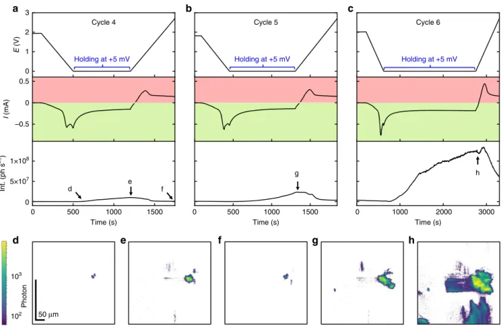
Figure4shows the E, I, and Int curves for cycle 4, 5, and 6 as well as the corresponding FFDXM images. The entire 100 × 430 μm2FoV is shown. The two individual defects (Fig.4d) merged
into a large single defect at the end of the 4th lithiation cycle (Fig.4e). New defects were also formed, as a result of prolonged lithiation by holding the electrode potential at+5 mV (Fig.4e). These newly formed defects were, at this point, mainly elastic as confirmed by the vanished contrast after delithiation (Fig.4f). At the end of the 6th cycle, deformed Si was observed to cover consistently ~20% of the sample surface area (Supplementary Fig. 3). We note that the two early-stage defects, despite being barely noticeable when initially formed (Fig.2d), were responsible for the strongest structural defect (Fig.4h) within the FoV, both in terms of physical size and amplitude of deformation. For discussion on the evolution of the defect density upon cycling, the readers are kindly referred to Supplementary Fig. 3.
Operando AFM studies of the SEI layer. Operando FFDXM offers an unobstructed view to the defect formation in the buried
Si/LixSi interface, which is inaccessible to most surface probing
techniques. However, as a diffraction method it is insensitive to the amorphous SEI layer above. Operando study of the SEI layer is equally important as it governs the lithium-ion transport in and out of the Si electrodes. Furthermore, the early-stage defects (Fig. 2d) were only observed after the initial formation of the SEI layer, which points to a possible correlation. To complement the FFDXM measurements, operando AFM was performed on the same batch of Si electrodes. The high surface sensitivity of the AFM enables direct observation of the SEI formation at the surface of pristine single-crystal Si electrodes. The experimental setup for operando AFM is schematically shown in Supplemen-tary Fig. 4a. Peak-force quantitative-nano-mechanical (PF-QNM) mode23with a low contact force of 80 nN was used to minimize the disturbance of the AFM tip on the SEI formation.
Topography of the pristine single-crystal Si electrode at Eocp
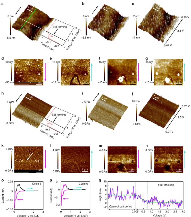
(Supplementary Fig. 5) reveals a typical smooth Si surface with a root mean square (RMS) roughness of 1.2 nm. Operando topographical measurements (Fig. 5a) of the same Si electrode were performed by scanning the electrode potential from Eocp
(~3.0 V) to +5 mV with a scan rate of 7 mV s−1 while moving simultaneously the AFM tip in the direction indicated by the black arrow. The operation principles for operando AFM is shown in Supplementary Fig. 4b–e. The corresponding current–voltage curve is shown in Fig. 5a. A SEI-free Si surface was observed up until E= 1 V. The surface became rougher starting at 0.75 V, signaling the beginning of the SEI formation. This was also evident from the surface height profile (Fig. 5q) generated by subtracting the height of the pristine Si surface (green line in Supplementary Fig. 5) from that of the operando measurements (green line in Fig. 5a). It can be seen that SEI
102 50 µm E (V) I (mA) Int. (ph s –1) 103 (5) d e f g h
Cycle 4 Cycle 5 Cycle 6
Time (s) Time (s) Time (s)
Photon 0 500 1000 1500 0 500 1000 1500 0 1000 2000 3000 0 5×10⁷ 1×10⁸ –0.5 0.5 0 0 1 2 3 a b c d
Holding at +5 mV Holding at +5 mV Holding at +5 mV
e f g h
Fig. 4 Defect evolution from cycle 4 to 6.E, I, and Int curves of cycle 4 (a), 5 (b), and 6 (c). The light green and light red background illustrate the current range for lithiation (negative currents) and delithiation (positive currents), respectively. The labels ofd–h match the marked annotations in a–c, corresponding to the instants of time at which the FFDXM images were taken.
–5.5 nm Current (mA) Current (mA) Voltage (V vs. Li/Li +) Voltage (V vs. Li/Li +) 6 nm –5.5 nm 6 nm 1 µ m 1 µm 1 µ m –7 nm 7 nm –30 nm 30 nm –15 nm 15 nm –15 nm 15 nm –15 nm 15 nm 1 µm 1 µm 1 µm 0.07 V 2.5 V 0.75 V a b c d e f g –0.2 –0.1 0 0.1 Current (mA) Cycle 6 Voltage (V vs. Li/Li+) 3 2 1 0 Voltage (V vs. Li/Li+) 3 2 1 0 –0.10 –0.05 0 0.05 Current (mA) o p Cycle 5 0 –0.1 –0.2 3 2 1 0 0 GPa 0.07 V 2.5 V 0.75 V 7 GPa 0 GPa 7 GPa 0 GPa 6 GPa 0 GPa 4 GPa 0 GPa 4 GPa 0 GPa 4 GPa 0 GPa 3 GPa h i j k l m n 0 –0.1 –0.2 3 2 1 0 SEI forming SEI forming q Voltage (V) 0.005 0.5 1.0 1.5 2.0 2.5 3.0 –2 0 2 4 6 8 Height (nm) Open-circuit period 10 1 µm 1 µm 1 µm 1 µm 1 µm First lithiation 1 µ m 1 µ m 1 µm
Fig. 5 Operando AFM measurements on the single-crystal Si electrode. Topographical map and current–voltage curve during the first CV scan from Eocp
to the cut-off potential of+5 mV at a scan rate of 7 mV s−1(a), during the resting period (b), during the CV scan back to 2.5 V and down to 0.75 V (c). d and e are the topographic maps during the 5th CV cycle. f and g are the topographic maps during the 6th CV cycle. The current and voltage for d, e and forf, g are indicated respectively by the colored curve in o and p. The colored arrows to the right of each map indicate the direction of the topographic scans (d–g). Also shown are results of Young’s modulus measurements. The Young’s modulus maps in h–n are taken at the same time as the topographic maps ina–g, respectively. The missing data in d and k are caused by surface fluctuations during the crack formation. q shows the height profile of the surface during thefirst lithiation and subsequent open-circuit period.
started to develop when the sample was scanned at the SEI forming potential of 0.75 V. The current was switched off as soon as the electrode potential reached+5 mV. During the subsequent open-circuit period a complete topographical image was taken (Fig. 5b). The result shows that the surface was covered by an inhomogeneous SEI layer with an RMS roughness of 2.4 nm. Figure 5c shows the topographical AFM image during the scan back to 2.5 V and then down to 0.75 V.
To mimic the same conditions as in the FFDXM experiments, more CV cycles were applied. The SEI formation peak was not so pronounced in subsequent cycles as compared with thefirst one, consistent with the FFDXM observation. A triangular-shaped crack (Fig. 5e) was observed while scanning the electrode potential from +5 mV back to 2.5 V during the 5th cycle. The scanning periods for Fig.5d, e are indicated by the magenta and turquoise curve in Fig. 5o, respectively. Due to this crack formation, the contact of the AFM tip with sample surface was lost for a brief period of time, as recognized by the blurry region in the lower part of Fig.5d. The sample was further scanned for the 6th cycle. The scanning periods for Fig.5f, g are indicated by the magenta and turquoise curve in Fig.5p, respectively. New SEI was formed, as indicated by the bright contrast in Fig. 5f, g. In particular, a large bright spot was observed on top of the triangle-shaped cracked area found in Fig.5e.
To understand the origin of the crack formation, Young’s modulus or the stiffness of the electrode surface was measured while performing operando topographical measurements in the PF-QNM mode. Figure 5h–j shows the operando Young’s modulus map of the Si electrode surface during the first CV cycle, measured simultaneously as the topographical images shown in Fig.5a–c, respectively. Figure5h clearly shows that the sample surface became harder when the potential reached the SEI forming potential at 0.75 V. Figure 5i shows that the entire
sample surface was covered by a layer of hard SEI materials during the open-circuit period. When the Si electrode was scanned back from 5 mV to 2.5 V, the sample surface subse-quently became softer (Fig. 5j), the reason of which will be discussed in the next section.
The stiffness of the sample surface continued to decrease in the subsequent cycles. Figure5k–n shows the Young’s modulus maps of the 5th and 6th cycle, measured simultaneously as the topographical images shown in Fig.5d–g, respectively. The crack was also clearly visible in the Young’s modulus maps. Local hardening was observed at the upper corner of the triangular-shaped crack (Fig. 5m). The hardened areas manifested themselves as brighter contrast on the Young’s modulus maps and were observed even before the cracking in Fig. 5k (white arrow). The connection between the AFM observations (local hardening to crack) and the FFDXM observations (early-stage to large-scale defects) will be discussed later. As the crack broke the SEI layer, new SEI was formed on freshly exposed Si in contact with the liquid electrolyte. It is worth mentioning that the newly formed SEI contains a high ratio of soft materials as indicated by the darker contrast on the Young’s modulus maps (Fig.5m, n). Inhomogeneity of lithium-ion mobility in dual-layer SEI. From the operando Young’s modulus maps, it can be inferred that the SEI layer formed during the 1st lithiation (Fig. 5i) was harder than that formed during subsequent cycles (e.g., Fig.5j). This is because of the duality nature of the SEI. Similar to what was found on carbon-based electrodes24–27, the SEI on Si also has a
dual-layer structure, composed of an inner- and outer-SEI layer28–30. The so-called inner SEI mainly consists of inorganic
species which are dense, thin, and relatively stable24,31,32. A
so-called outer-SEI layer is formed on top of the inner-SEI layer, and C–C C–H C–O–C ROCO2Li Li2CO3 Li2O LiF ROCO2Li Li2CO3 280 c 284 288 292 52 54 56 58
Binding energy (eV) Binding energy (eV)
280 284 288 292 52 54 56 58
Binding energy (eV) Binding energy (eV)
Intensity (a.u.) Intensity (a.u.)
Li 1s C 1s 0.20 0.51 Amplitude (a.u.) Li 1s C 1s 0 0
Intensity (a.u.) Intensity (a.u.)
d g h 200 nm Percentage (%) 0 1 2 3 0.20 0.90 Amplitude (a.u.) 200 nm e f Amplitude (a.u.) Percentage (%) 0.2 0.4 0.6 0.8 Amplitude (a.u.) 0.2 0.4 0.6 0.8 0 1 2 3 a b Outer-SEI Inner-SEI
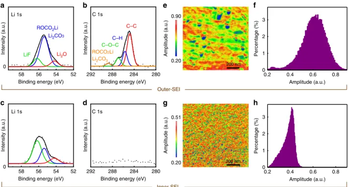
Fig. 6 Composition and lithium-ion mobility of the dual-layer SEI. Li 1s and C 1s sputter-etched XPS spectra of the Si electrode after the 6th cycle. The spectra ina and b were obtained without sputter-etching the SEI surface and represent the chemical information of the outer-SEI layer. The spectra in c and d were recorded after about 10 s of sputter-etching and represent the chemical information of the inner-SEI layer. ESM amplitude map (e) and corresponding histogram (f) of the Si electrode after the 6th cycle. ESM amplitude map (g) and corresponding histogram (h) of another Si electrode, after being scanned to +5 mV during its first CV cycle at a scan rate of 7 mV s−1. The center contact resonance frequency of the tip-sample system was 290 kHz for the two ESM
measurements.
is mainly composed of organic material, which continues to grow upon cycling24,28.
Sputter-etched XPS analyses have been performed to study the chemistry of the inner- and outer-SEI layers. Figure 6a–d shows the Li 1s and C 1s spectra of the dismantled sample (rinsed by DMC and dried) after the 6th CV cycle. The spectra in Fig.6a, b are collected without sputter-etching the surface and are therefore representative of the outer-SEI layer. The result (Li 1s spectra, Fig.6a) confirmed that the outer SEI mainly comprised of organic species, such as ROCO2Li (where R is a low-molecular-weight
alkyl group)33–35. Figure 6b shows intensive peaks of multiple carbon-based species in the C 1s spectra. The predominant presence of organic materials leads to a softer outer-SEI layer as observed in the Young’s modulus maps (Fig. 5j–n). Small amounts of LiF and Li2O were also observed in the outer-SEI
layer, albeit significantly less than ROCO2Li (Fig.6a). Figure6c, d
shows the spectra collected after about 10 s of sputter-etching and are representative of the inner-SEI layer. In sharp contrast, inorganic LiF was found to be the dominant component (Fig.6c) with a significantly weaker presence of the carbon species (Fig.6d). The result explains the origin of the harder inner-SEI layer as observed in the Young’s modulus map (Fig.5i).
Result of 3D RSM (Fig.3) indicated heterogeneous lithiation to be responsible for the formation of the early-stage defects. The heterogeneous lithiation is likely to be caused by an inhomoge-neous conduction of the lithium-ion in the SEI layer. To verify this, ex situ ESM was employed on the Si electrode after it was dismantled at the end of the 6th CV cycle. The electrode surface was subsequently rinsed by DMC and dried. The ESM amplitude is a measurement of the electrical-field-induced surface strain and is proportional to the lithium-ion mobility36–38. Figure 6e, f shows the ESM amplitude map and corresponding histogram. The ESM map in Fig.6e shows a strong variation in lithium-ion mobility with some areas of the sample conducting lithium-ion more than four times less than some other areas. It is worth noting that the inhomogeneous lithium-ion mobility observed in Fig.6e is characteristic of the outer-SEI layer. Ex situ ESM was also performed on the inner-SEI layer. This latter was made possible by dismantling another Si electrode after it was scanned to+5 mV in its 1st cycle. The Young’s modulus measurement in Fig. 5i indicated that the Si electrode at this stage was only covered by the inner SEI. Figure6g, h shows the ESM amplitude map and corresponding histogram. The results revealed that the lithium-ion mobility of the inner SEI was also inhomogeneous, albeit with a weaker variation.
Discussion
The impact of the SEI on the structural deformation in Si elec-trodes was studied by a combination of operando and ex situ techniques. For operando studies, CV with a relatively fast scan rate of 5 mV s−1 was used to intentionally limit the amount of lithiation during each cycle. This allowed us to observe the for-mation of defects at a mere 0.1–0.2% of the total lithiation capacity of Si. We refer to them as early-stage defects because of their low density (<100 ppm, Supplementary Fig. 3) and weak amplitude of deformation (Fig. 3a), making them essentially invisible to nonlocal techniques that average over the entire sample (Supplementary Fig. 2). Spontaneous relaxation was observed both during lithiation and delithiation, and the defor-mation around the early-stage defects was found to be mainly elastic (Fig.2k). The significance of these early-stage defects was later revealed by prolonging the potential holding at +5 mV, during which both the defect density and their amplitude of deformation gradually increased. It was shown that, of the ~20% surface area (Supplementary Fig. 3f) covered by
large-scale defects, the most deformed part was evolved from the early-stage defects. In other words, suppressing the formation of early-stage defects is essential to improving the structural stability of Si electrodes upon cycling.
3D RSM result at the end of cycle 3 shows the lattice in the defective area to be tilting inwards (Fig.3a), indicating locally a lower degree of lithiation compared with the surrounding area. This heterogeneous lithiation is likely to be caused by two major factors: inhomogeneities in the thickness of the lithium-ion-conducting SEI layer (longer transportation time for thicker regions) and in the mobility of the lithium-ion (less conducting for lower mobility). Both were supported by the present study. On one hand, operando topographic measurement showed a twofold increase in RMS roughness (standard deviation of layer thickness) in the initially formed SEI (Fig.5b). On the other hand, ex situ ESM (Fig.6e) result revealed a strong variation in lithium-ion mobility of the SEI layer, with some areas of the sample conducting lithium-ion more than four times less than other areas. These inhomogeneities inevitably led to a heterogeneous degree of lithiation, which in turn resulted in the lattice defor-mation as seen by FFDXM. To further confirm this correlation, we have performed FFDXM experiments on the same batch of Si samples coated with a homogeneous artificial SEI (Li4Ti5O12
-Li3PO4). Indeed, no defects were ever observed under similar
cycling conditions. This last result can be found in Supplementary Fig. 6.
The SEI formed on Si is known to have a dual-layer structure, composed of a softer (Fig.5j–n) and mainly organic (Fig. 6a, b) outer-SEI layer on top of a harder (Fig.5i) and mainly inorganic (Fig.6c, d) inner-SEI layer. We note that the average lithium-ion mobility of the outer-SEI layer (Fig. 6f) is ~1.5 times that of the inner one (Fig. 6h), which is explained by a higher lithium-ion conductivity for Li2CO3and ROCO2Li (main components of the
outer SEI) than for LiF (main component of the inner SEI)39–42. This indicates that the lithium-ion transport through the inner SEI is the major limiting factor in the case of Si electrodes. Optimizing the thickness and roughness of the inner SEI is thus more rewarding than tuning those of the outer one. The prop-erties of the inner SEI are known to be affected by the surface of the electrode, due to their direct contact. As is the case for this study, the presence of native silicon oxide promotes the formation of a less rough and thinner SEI43,44. The use of rigid Si wafers
with atomicallyflat surface also helps reduce the roughness of the SEI layer, which is favorable for observing the defects in their early stage.
Although operando FFDXM and AFM were not performed simultaneously on the same sample, the two observations were closely connected. The early-stage defects first appeared during the 2nd cycle in the FFDXM experiments (Fig. 2b, d). In the meantime, local (i.e., inhomogeneous) hardening of the Si elec-trode was also observed during the 2nd cycle in the AFM experiment. The local hardening manifests itself as brighter contrast in the Young’s modulus map (black square, Supple-mentary Fig. 7c) and is explained by a local variation in the chemical composition. More importantly, FFDXM showed that after extensive cycling, the part where the Si lattice was most deformed lies on top of the early-stage defects (Fig.4). Similarly, the cracking of the Si electrode observed by AFM (Fig.5k–n) is also tied to the local hardened area. It is worth noting that the mismatch in spatial resolution and FoV between the FFDXM and AFM is in fact welcomed. The deformation in the lattice often extends much further than the physical size of the defects. The 100-nm spatial resolution of FFDXM is adequate for the inves-tigation of the nature of the defects because their lattice defor-mation has the size of roughly 4 × 4μm2(Fig.3a). Its large FoV
were initially formed. AFM, on the other hand, measures the physical size of the defects. Itsfiner spatial resolution (20 nm) is required to resolve the crack (1 × 1 μm2) and the topographic
inhomogeneities (0.1 × 0.1μm2, Fig.5).
Our multimodal study bridges the gap between conventional X-ray diffraction, sensitive to structural deformation but not in its early stage (i.e., <100 ppm) and surface probing microscopy which measures topography, stiffness, lithium-ion mobility but not in buried layers. It reveals the presence of the early-stage defects and their ominous connection to the large-scale defor-mation causing mechanical failures in the electrodes. We note that the onset of the early-stage defects and their evolution have been consistently observed over repeated experiments, and under various cycling conditions (Supplementary Fig. 8). The present study allows us to construct a model (Supplementary Movie 3) that highlights the inhomogeneities in the dual-layer SEI and their correlation to the structural deformation inside Si electrodes in liquid electrolyte. This correlation may, for instance, explain the unexpected yet consistent crack observations in extremely thin (20 nm) Sifilm electrodes18,45, despite a theoretical critical
thickness of 100 nm18,46. More generally, we hope to accentuate the importance of minimizing the inhomogeneities in the SEI (natural or artificial) on improving the structural stability of Si-based LIB.
Methods
Electrodes preparation. Single-crystal Si electrodes were fabricated by thermal evaporating 200 nm Cu on one side of highly doped, double-side polished, (100) oriented Si wafers (200 µm thick, UniversityWafer), acting as the current collector. The rigidness of the thick Si substrates is necessary for high-precision measure-ments of the structural deformation. Free standing thinfilms are not recommended as they are often bent (inherent lattice tilt) due to the absence of a rigid support, and easily strained (inherent lattice strain) by adhesives. The Si near the surface participates in the (de)lithiation process and is subsequently amorphized, the dark-field contrast in FFDXM thus reflects structural changes in single-crystal pristine Si just below the Si/LixSi interface.
Operando FFDXM. FFDXM experiments were carried out on the ID01 beamline at the European synchrotron radiation facilities (ESRF) in Grenoble, France. The size of the Si samples was 7 × 5 mm2. The custom-made 3-electrode electrochemistry
cell is controlled by a potentiostat (Biologic, SP300). 1 M LiPF6dissolved in EC/
DMC (1:1 in volume ratio) was used as electrolyte. All potentials are given with respect to the Li/Li+reference electrode.
FFDXM is a novel synchrotron technique that combines X-ray diffraction with spatially resolved microscopy. The basic principles of FFDXM time-scan and 3D RSM are schematically shown in Supplementary Fig. 9. The Si samples were mounted vertically so that the surface normal lies in the horizontal scattering plane (the X–Y plane, Supplementary Fig. 9a). The illuminated sample area is 980 (H) × 240 (V)μm2. The pre-focusing by the in vacuum Beryllium transfocator at 62-m
upstream of the sample allows a high incoming photonflux to be achieved with a near parallel beam (convergence < 0.03 mrad). A set of CRLs (SU-8, made by the Karlsruhe Institute of Technology, 6μm apex radius of curvature47) was mounted
behind the sample to image the diffracted beam. For each point of data acquisition, a real space image (raw FFDXM image) was acquired on the area detector (Andor Zyla 5.5 sCMOS, 6.5μm pixel size, 2560 × 2160 pixels), which is direct fiber-coupled to a 15μm of Gadox scintillator. The X-ray energy for the experiments was chosen to be 19.7 keV to reduce absorption from the operando electrochemical cell and the electrolyte. For the operando measurements, the so-called time scans were performed at a sample angle−0.03° off the θ angle for the (004) reflection (tilted by the phi motor). Supplementary Fig. 9b shows the integrated Int of a rocking curve around the (004) Si reflection. The full width at half maximum is broadened by the bandwidth of the multilayer monochromator (ΔE/E = 3 × 10⁻³). At−0.03° off the
Bragg angle (marked by the arrow in Supplementary Fig. 9b), the technique is highly sensitive to any deformation of Si, deviating from the perfect single-crystal structure. For the 3D RSM, the sample was scanned in three orthogonal directions in the reciprocal space, given respectively by the phi rocking, the psi rocking, and the Q (the momentum transfer) direction (Supplementary Fig. 9c). The two sample rocking motions allow the lattice tilt to be mapped at a resolution of 10−2mrad, whereas the radial motion in the Q direction (achieved via aθ–2θ motion by moving simultaneously the sample phi, the detector, and the lenses) allows the lattice strain to be mapped at a resolution of 10−4.
Operando AFM. An AFM (Bruker, Santa Barbara, USA, Dimension Icon Micro-scope) setup, operating inside an Argon-filled glove box (H2O < 0.1 ppm, O2< 0.1
ppm, MBraun, Stratham, USA), was used to perform the operando AFM mea-surements. The design of the in-house made cell holder for the AFM measurements is shown in Supplementary Fig. 4a. The Si single-crystal working electrode is assembled in the AFM cell with two lithium metal foils, acting as the RE and the CE and 1 M LiPF6dissolved in 1:1 EC/DMC as the electrolyte. PF-QNM mode23
was employed to carry out the topographical investigations. Tapping mode can-tilevers (NCHR, NanoSensors) made of doped silicon with a nominal spring constant of 64 nN nm−1were used as force transducer. All images have been captured with a tip-force of 80 nN at a scan rate of 0.5 Hz in the trace–retrace mode. The direction of the tip movement is indicated in each image. All AFM images are recorded with a pixel density of 256 data points per line. Electrochemical strain microscopy (ESM). For lithium-ion movability detec-tions, the AFM was operated in the ESM mode, which is effective to qualitatively visualize local variations36,37. ESM, conducted in the contact mode, is a novel AFM
technique. It concentrates a periodic electricalfield with the same frequency as the contact resonance frequency at the conductive AFM tip within a radius of about 10 nm36,37. The induced electricalfield then moves lithium ions toward or away
from the electrode surface38. This results in local electrochemical surface strain,
which is proportional to the local lithium-ion mobility36,37. In the ESM mapping
mode, the cantilever was changed to a conductive one with a platinum/iridium coating (PPP-EFM, Nanosensors) and a nominal spring constant of 2.8 N m−1. The contact resonance frequency and amplitude were tracked with a phase-locked loop (HF2LI, Zurich Instruments, Switzerland). This ensures that frequency shifts during the measurement are tracked and measurements are always on resonance. The center frequency is given in the various ESM-relatedfigure captions. To ensure a stable tip-sample interaction, a slow scanning frequency of about 1.5 Hz was applied with 256 data points per line and a drive amplitude of 2 V. The two ESM measurements were performed in trace and retrace mode with the same parameters by using identical tip.
Sputter-etched XPS. XPS spectra were obtained with a ThermoScientific K-Alpha instrument equipped with a monochromatic X-ray source (Al Kα = 1486.6 eV). The Si sample after 6 CV cycles was etched at an input power of 300 W, a gas pressure of 30 mTorr, and a gasflow of 8% oxygen content. All samples were transferred in a shuttle transfer system under Ar from the glove box (Unilab PRO, MBraun) to the FFDXM, AFM, ESM, and XPS equipment.
Data availability
The data that support the graphs within this paper and otherfindings of this study are available from the corresponding author upon reasonable request.
Received: 2 December 2019; Accepted: 13 June 2020;
References
1. Armand, M. & Tarascon, J.-M. Building better batteries. Nature 451, 652–657 (2008).
2. Chan, C. K. et al. High-performance lithium battery anodes using silicon nanowires. Nat. Nanotechnol. 3, 31–35 (2008).
3. Notten, P. H. L., Roozeboom, F., Niessen, R. A. H. & Baggetto, L. 3-D integrated all-solid-state rechargeable batteries. Adv. Mater. 19, 4564–4567 (2007).
4. Jiménez, A. R. et al. A step toward high-energy silicon-based thinfilm lithium ion batteries. ACS Nano 11, 4731–4744 (2017).
5. Wen, C. J. & Huggins, R. A. Chemical diffusion in intermediate phases in the lithium-silicon system. J. Solid State Chem. 37, 271–278 (1981).
6. McDowell, M. T., Lee, S. W., Nix, W. D. & Cui, Y. 25th anniversary article: understanding the lithiation of silicon and other alloying anodes for lithium-ion batteries. Adv. Mater. 25, 4966–4985 (2013).
7. Baggetto, L., Niessen, R. A. H. & Notten, P. H. L. On the activation and charge transfer kinetics of evaporated silicon electrode/electrolyte interfaces. Electrochim. Acta 54, 5937–5941 (2009).
8. Bridel, J.-S., Azaïs, T., Morcrette, M., Tarascon, J.-M. & Larcher, D. In situ observation and long-term reactivity of Si/C/CMC composites electrodes for Li-ion batteries. J. Electrochem. Soc. 158, A750–A759 (2011).
9. Chen, C. et al. Origin of degradation in Si-based all-solid-state Li-ion microbatteries. Adv. Energy Mater. 8, 181430 (2018).
10. Liu, X. H. et al. Anisotropic swelling and fracture of silicon nanowires during lithiation. Nano Lett. 11, 3312–3318 (2011).
11. Lee, S. W., McDowell, M. T., Berla, L. A., Nix, W. D. & Cui, Y. Fracture of crystalline silicon nanopillars during electrochemical lithium insertion. Proc. Natl Acad. Sci. U. S. A. 109, 4080–4085 (2012).
12. Goldman, J. L., Long, B. R., Gewirth, A. A. & Nuzzo, R. G. Strain anisotropies and self-limiting capacities in single-crystalline 3D silicon microstructures: models for high energy density lithium-ion battery anodes. Adv. Funct. Mater. 21, 2412–2422 (2011).
13. Pharr, M., Suo, Z. & Vlassak, J. J. Measurements of the fracture energy of lithiated silicon electrodes of Li-ions batteries. Nano Lett. 13, 5570–5577 (2013). 14. Zeng, Z. et al. In situ measurement of lithiation-induced stress in silicon
nanoparticles using micro-raman spectroscopy. Nano Energy 22, 105–110 (2016). 15. Tardif, S. et al. Operando raman spectroscopy and synchrotron X-ray
diffraction of lithiation/delithiation in silicon nanoparticle anodes. ACS Nano 11, 11306–11316 (2017).
16. Zhao, K. et al. Concurrent reaction and plasticity during initial lithiation of crystalline silicon in lithium-ion batteries. J. Electrochem. Soc. 159, A238–A243 (2012).
17. Liu, X. H. et al. Size-dependent fracture of silicon nanoparticles during lithiation. ACS Nano 6, 1522–1531 (2012).
18. Wu, Q. et al. Investigation of Si thinfilms as anode of lithium-ion batteries. ACS Appl. Mater. Interfaces 10, 3487–3494 (2018).
19. Hilhorst, J., Marschall, F., Tran Thi, T. N., Last, A. & Schülli, T. U. Full-field X-ray diffraction microscopy using polymeric compound refractive lenses. J. Appl. Crystallogr 47, 1882–1888 (2014).
20. Leake, S. J. et al. The nanodiffraction beamline ID01/ESRF: a microscope for imaging strain and structure. J. Synchrotron Radiat. 26, 571–584 (2019). 21. Bagetto, L., Niessen, R. A. H., Roozeboom, F. & Notten, P. H. L. High energy
density all-solid-state batteries: a challenging concept towards 3D integration. Adv. Funct. Mater. 18, 1057–1066 (2008).
22. Xu, K. Nonaqueous liquid electrolytes for lithium-based rechargeable batteries. Chem. Rev. 104, 4303–4418 (2004).
23. Pletikapić, G., Berquand, A., Radić, T. M. & Svetličić, V. Quantative nanaomechanical mapping of marine diatom in seawater using peak force tapping atomic force microscopy. J. Phycol. 48, 174–185 (2012).
24. Peled, E. & Menkin, S. Review-SEI: past, present and future. J. Electrochem. Soc. 164, A1703–A1719 (2017).
25. Edström, K., Herstedt, M. & Abraham, D. P. A new look at the solid electrolyte interphase on graphite anodes in Li-ion batteries. J. Power Sources 153, 380–384 (2006).
26. Li, D. et al. Degradation mechanisms of C6/LiNi0.5Mn0.3Co0.2O2Li-ion
batteries unraveled by non-destructive and post-mortem methods. J. Power Sources 416, 163–174 (2019).
27. Li, D. et al. Modeling the SEI-formation on graphite electrodes in LiFePO4
batteries. J. Electrochem. Soc. 162, A858–A869 (2015).
28. Zhang, Y., Du, N. & Yang, D. Design superior solid electrolyte interface on silicon anodes for high-performance lithium-ion battery. Nanoscale 11, 19086–19104 (2019).
29. Zheng, J. et al. 3D visualization of inhomogeneous multi-layered structure and Young’s modulus of the solid electrolyte interphase (SEI) on silicon anodes for lithium ion batteries. Phys. Chem. Chem. Phys. 16, 13229–13238 (2014). 30. Wang, A., Kadam, S., Li, H., Shi, S. & Qi, Y. Review on modeling of anode
solid electrolyte interphase (SEI) for lithium-ion batteries. Npj Comput. Mater. 4, 15 (2018).
31. Benitez, L., Cristancho, D., Seminario, J. M., Martinez de la Hoz, J. M. & Balbuena, P. B. Electron transfer through solid-electrolyte-interphase layers formed on Si anodes of Li-ion batteries. Electrochim. Acta 140, 250–257 (2014).
32. Soto, F. A., Ma, Y., Martinez de la Hoz, J. M., Seminario, J. M. & Balbuena, P. B. Formation and growth mechanisms of solid-electrolyte interphase layers in rechargeable batteries. Chem. Mater. 27, 7990–8000 (2015).
33. Verma, P., Maire, P. & Novák, P. A review of features and analyses of the solid electrolyte interphase in Li-ion batteries. Electrochim. Acta 55, 6332–6341 (2010).
34. Yang, L. et al. Changing of SEIfilm and electrochemical properties about MCMB electrodes during long-term charge/discharge cycles. J. Electrochem. Soc. 160, A2093–A2099 (2013).
35. Guan, P., Liu, L. & Lin, X. Simulation and experiment on solid electrolyte interphase (SEI) morphology evolution and lithium-ion diffusion. J. Electrochem. Soc. 162, A1798–A1808 (2015).
36. Balke, N. et al. Nanoscale mapping of ion diffusion in a lithium-ion battery cathode. Nat. Nanotechnol. 5, 749–754 (2010).
37. Kalinin, S. et al. Li-ion dynamics and reactivity on the nanoscale. Mater. Today 14, 548–558 (2014).
38. Schӧn, N. et al. Correlative electrochemical strain and scanning electron microscopy for local characterization of the solid state electrolyte Li1.3Al0.3Ti1.7(PO4)3. Beilstein J. Nanotechnol. 9, 1564–1572 (2018).
39. Shi, S., Qi, Y., Li, H. Jr. & Hector, LG. Defect thermodynamics and diffusion mechanisms in Li2CO3and implications for the solid electrolyte interphase in
Li-ion batteries. J. Phys. Chem. C. 117, 8579–8593 (2013).
40. Borodin, O., Zhang, G. V., Ross, P. N. & Xu, K. Molecular dynamics simulations and experimental study of lithium ion transport in dilithium ethylene dicarbonate. J. Phys. Chem. C. 117, 7433–7444 (2013). 41. Bedrov, D., Borodin, O. & Hooper, J. B. Li+transport and mechanical
properties of model solid electrolyte interphases (SEI): insight from atomistic molecular dynamics simulations. J. Phys. Chem. C. 121, 16098–16109 (2017). 42. Pan, J., Cheng, Y.-T. & Qi, Y. General method to predict voltage-dependent
ionic conduction in a solid electrolyte coating on electrodes. Phys. Rev. B 91, 134116 (2015).
43. Schroder, K. W., Dylla, A. G., Harris, S. J., Webb, L. J. & Stevenson, K. J. Role of surface oxides in the formation of solid-electrolyte interphases at silicon electrodes for lithium-ion batteries. ACS Appl. Mater. Interfaces 6, 21510–21524 (2014).
44. Cao, C. et al. Solid electrolyte interphase on native oxide-terminated silicon anodes for Li-ion batteries. Joule 3, 762–781 (2019).
45. Lee, S.-J. et al. Stress effect on cycle properties of the silicon thin-film anode. J. Power Sources 97–98, 191–193 (2001).
46. Réthoré, J., Zheng, H., Li, H., Li, J. & Aifantis, K. E. A Multiphysics model that can capture crack patterns in Si thinfilms based on their microstructure. J. Power Sources 400, 383–391 (2018).
47. Marschall, F., Last, A., Simon, M., Vogt, H. & Mohr, J. Simulation of aperture-optimised refractive lenses for hard X-ray fullfield microscopy. Opt. Express 24, 10880–10889 (2016).
Acknowledgements
The authors are grateful to the ESRF for providing beam time at ID01. C.C. acknowl-edges the Chinese Scholarship Council (Grant No. 201506020080) for partiallyfinancial support of this work. T.Z. acknowledges support from the Center for Nanoscale Mate-rials, a U.S. Department of Energy Office of Science User Facility under Contract No. DE-AC02-06CH11357. T.Z. would like to thank Jakub Drnec and Manuel Marechal for the helpful discussions.
Author contributions
C.C. and T.Z. contributed equally to this work. C.C. and T.Z. conceived the idea and conducted most of the experimental work. C.C. has fabricated the samples. C.C. has analyzed the samples by operando AFM, ESM, and XPS with the assistance of S.B., N.S., and L.G. C.C., T.Z., D.L.D., and P.H.L.N. composed the manuscript with the comments from all authors. T.Z. analyzed the FFDXM data. D.L.D., S.T., H.S., F.H., T.U.S., R.-A.E., and P.H.L.N. contributed to the scientific discussions.
Competing interests
The authors declare no competing interests.
Additional information
Supplementary informationis available for this paper at
https://doi.org/10.1038/s41467-020-17104-9.
Correspondenceand requests for materials should be addressed to C.C. or P.H.L.N. Peer review informationNature Communications thanks Andrea Somogyi and the other, anonymous, reviewer(s) for their contribution to the peer review of this work. Peer reviewer reports are available.
Reprints and permission informationis available athttp://www.nature.com/reprints
Publisher’s note Springer Nature remains neutral with regard to jurisdictional claims in published maps and institutional affiliations.
Open Access This article is licensed under a Creative Commons Attribution 4.0 International License, which permits use, sharing, adaptation, distribution and reproduction in any medium or format, as long as you give appropriate credit to the original author(s) and the source, provide a link to the Creative Commons license, and indicate if changes were made. The images or other third party material in this article are included in the article’s Creative Commons license, unless indicated otherwise in a credit line to the material. If material is not included in the article’s Creative Commons license and your intended use is not permitted by statutory regulation or exceeds the permitted use, you will need to obtain permission directly from the copyright holder. To view a copy of this license, visithttp://creativecommons.org/
licenses/by/4.0/.