EUROPEAN ORGANISATION FOR NUCLEAR RESEARCH (CERN)
Submitted to: JINST CERN-EP-2020-232
14th January 2021
The ATLAS Fast TracKer system
The ATLAS Collaboration
The ATLAS Fast TracKer (FTK) was designed to provide full tracking for the ATLAS high-level trigger by using pattern recognition based on Associative Memory (AM) chips and fitting in high-speed field programmable gate arrays. The tracks found by the FTK are based on inputs from all modules of the pixel and silicon microstrip trackers. The as-built FTK system and components are described, as is the online software used to control them while running in the ATLAS data acquisition system. Also described is the simulation of the FTK hardware and the optimization of the AM pattern banks. An optimization for long-lived particles with large impact parameter values is included. A test of the FTK system with the data playback facility that allowed the FTK to be commissioned during the shutdown between Run 2 and Run 3 of the LHC is reported. The resulting tracks from part of the FTK system covering a limited 𝜂–𝜙 region of the detector are compared with the output from the FTK simulation. It is shown that FTK performance is in good agreement with the simulation.
© 2021 CERN for the benefit of the ATLAS Collaboration.
Reproduction of this article or parts of it is allowed as specified in the CC-BY-4.0 license.
Contents
1 Introduction 3
2 FTK system overview 4
3 Hardware and firmware 8
3.1 Infrastructure and interface to the Pixel and SCT detectors 9
3.2 QuestNP 9
3.3 Input Mezzanine 10
3.4 Data Formatter 14
3.5 Auxiliary Card 17
3.6 Associative Memory Board 19
3.7 Associative Memory 21
3.8 Second Stage Board 23
3.9 FTK-to-High-Level-Trigger Interface Card 26
4 Online software, control and monitoring 28
4.1 Run Control integration 29
4.2 Automated procedures 29
4.3 Monitoring 30
5 Configuration, optimization and performance 30
5.1 Simulation 30
5.2 Sectors and constants 32
5.3 Pattern-bank production 32
5.4 Pattern-bank optimization 33
5.5 Production of a pattern bank for commissioning of the 128-PU system 34
5.6 Extension of the pattern bank to high-𝑑0tracks 35
5.7 Comparison of data and simulation 37
1 Introduction
The Fast TracKer (FTK) system [1] was foreseen as an evolution of the ATLAS experiment’s [2] trigger strategy designed to bring the tracking of charged particles into trigger decisions at the earliest possible point in the trigger algorithms. The ATLAS trigger [3,4] was originally designed around initial signatures based on energy deposits in the ATLAS calorimeters and the tracking of muons in the muon spectrometer (MS), which surrounds the calorimeters. In Runs 1–3 of the Large Hadron Collider (LHC) the ATLAS first-level (L1) trigger system uses hardware-based algorithms to reduce the 40 MHz rate from the beam-crossings to approximately 100 kHz, which can then be processed in the high-level trigger (HLT) to reduce the rate by another factor of 50 or more before recording events. In 2018, for example, the average event-recording rate was 1200 Hz [5]. Initially, in Run 1, the commodity-computing-based HLT was designed with a first step to process small areas around each of the L1 trigger objects. Within these regions-of-interest (RoIs), software-based tracking occurred as late as possible in the trigger algorithms to minimize the use of HLT resources. In many cases, the RoI approach led to significant inefficiencies, for example in jet finding,
because of differences between the online and offline strategies [6, 7]. In addition, the instantaneous
luminosity of the LHC increased to 2 × 1034cm−2s−1and the number of overlapping collisions, pile-up (𝜇), frequently exceeded 50, leading to large inefficiencies. The FTK was designed to mitigate this by using custom hardware to provide tracks to the HLT at the full L1 trigger rate for events with up to 80 pile-up collisions.
By reconstructing all charged particles in an event with transverse momentum (𝑝T) down to 1 GeV with
good efficiency, it is possible to use algorithms such as particle flow [8] to accurately separate the energy deposited in the target event from that of the pile-up interactions. Such techniques for pile-up mitigation are especially important for final states that require jets to be reconstructed and in events with signatures
involving missing transverse momentum (𝐸Tmiss) [9]. Examples of areas where ATLAS triggers would
benefit from full tracking down to low 𝑝Tinclude di-Higgs production with decays to the four-𝑏-quark final state [10] (tracks are also used to tag jets containing 𝑏-hadrons) and exotic [11] and/or supersymmetry [12] signatures involving 𝐸Tmiss. In addition, full reconstruction of charged tracks in an event, such as the FTK provides, allows for opportunistic use of these tracks in other signatures, e.g. 𝐵-physics, outside of RoIs or in other future scenarios.
The following sections present the as-built FTK system, along with the simulation and control software that was used for system commissioning at the end of Run 2 data-taking and during Long Shutdown 2 (LS2) before the project was stopped in 2019. The FTK system will not be used during Run 3. Instead, it is envisioned to perform more tracking in the HLT for signatures that benefit the most, e.g. jets and 𝐸Tmiss. A comparison of the performance of the hardware with simulation is presented. The paper is organized as
follows: an overview of the FTK system is described in Section2; the components of the FTK hardware,
including those used for the comparison, are described in more detail in Section3; the online software as
well as FTK control and monitoring are described in Section4; the FTK configuration, its optimization
using simulation and its performance in a vertical slice, a minimal set of electronics boards to process tracks, are described in Section5; and Section6contains the conclusion.
2 FTK system overview
The FTK system was developed to provide tracking of charged particles over the full acceptance of the ATLAS inner detector at the full L1 trigger rate of 100 kHz. It was designed to provide tracking information to the HLT, which operates asynchronously from the LHC clock. Tracking information from the FTK was provided to the HLT and the ATLAS data acquisition system [13] in the same manner as is used for detector readout. These systems do not require a fixed latency. The FTK uses four layers of hits from the silicon pixel (Pixel) system (including the insertable B-layer (IBL) [14,15] installed in 2015) and eight layers of hits from the four stereo pairs in the silicon microstrip (SCT) system for a total of twelve layers. The inner detector is surrounded by a thin superconducting solenoid providing a 2 T axial magnetic field; it covers the pseudorapidity range |𝜂| < 2.5 and full range in azimuthal angle 𝜙.1 Tracks in ATLAS are defined by five helix-parameters (𝑑0, 𝑧0, 𝑞/𝑝T, 𝜂, and 𝜙), where 𝑑0and 𝑧0are the transverse and longitudinal impact parameters respectively. Track quality can be assessed with a 𝜒2value from summing over the residuals of the hits and the track. The FTK system performs tracking in two steps. First, initial track candidates are found by using pattern recognition with eight layers of hits. Second, four additional layers of hits are added to the track and the track helix parameters are evaluated. The FTK system does not perform minimizations to fit tracks; instead, it evaluates a system of linear equations to perform a linearized track reconstruction. Challenges faced by the FTK system include handling, processing, buffering and synchronizing a high bandwidth of data on multiple parallel data paths (towers) in a large heterogeneous system with many interconnects; input hit organization across towers requiring duplication and sharing through multiple interconnects; creating, loading, and validating a large amount of configuration data for the pattern matching and track fitting; and managing and monitoring a large number of high-power-density electronics boards requiring active cooling.
At the core of the FTK is the content-addressable memory [16,17], the Associative Memory (AM) [18]
that performs the initial pattern recognition and forms candidate tracks to be processed further. The FTK AM is an ASIC specifically designed for the FTK system using a 65 nm CMOS technology. It is used to associate the data hits from the tracking detectors with stored patterns. The AM patterns use up to eight layers of hits (three Pixel and five SCT), which are binned with a variable granularity in the azimuthal angle and pseudorapidity. The AM layers were chosen to provide candidate tracks with a sufficient purity to allow downstream processing. The candidate tracks (roads) found by the AM pass a 𝜒2selection before proceeding to second-stage processing that extrapolates them to the innermost Pixel layer (the IBL) and to the three additional SCT layers. Figure1illustrates the track-finding algorithm used in the FTK, with more details described at the end of this section, after an overview of the FTK system components
The stages of processing in the FTK, clustering, data transport and sharing, pattern matching, and evaluations of track parameters in two stages, are summarized in Table1. These functions are spread across several electronics boards.
The Input Mezzanines (IMs), 128 cards mounted on the Data Formatter (DF) modules, have a total of 512 inputs. The IM cards cluster the hits from the Pixel and SCT sensors. The DF system, which consists of 32 ATCA [19] boards, routes the packets of hits corresponding to individual Pixel and SCT modules to an
1ATLAS uses a right-handed coordinate system with its origin at the nominal interaction point (IP) in the centre of the detector
and the 𝑧-axis along the beam pipe. The 𝑥-axis points from the IP to the centre of the LHC ring, and the 𝑦-axis points upwards. Cylindrical coordinates (𝑟, 𝜙) are used in the transverse plane, 𝜙 being the azimuthal angle around the 𝑧-axis. The pseudorapidity is defined in terms of the polar angle 𝜃 as 𝜂 = − ln tan(𝜃/2). Angular distance is measured in units of Δ𝑅 ≡√︁(Δ𝜂)2+ (Δ𝜙)2.
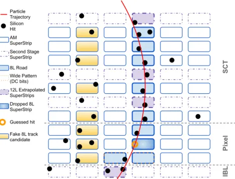
IBL Pixel SCT Silicon Hit Particle Trajectory AM SuperStrip Second Stage SuperStrip 8L Road 12L Extrapolated SuperStrips Dropped 8L SuperStrip Wide Pattern (DC bits) Fake 8L track candidate Guessed hit
Figure 1: Diagram of the track-finding method used in the FTK. Rounded boxes represent the coarse resolution SuperStrips used to bin the hits from the silicon detectors. Once eight layers (Associative Memory (AM) SuperStrips) with hits match a stored pattern they become a road (solid filled boxes), which is then extrapolated into the remaining four layers (dash-dot filled boxes). One layer may be dropped in the first eight layers used for pattern matching and another in the additional four layers. Fake track candidates (e.g. the gradient-filled boxes to the left) can be rejected because they have a large 𝜒2value or fail extrapolation to the additional four layers.
Table 1: Overview of the FTK system in the order in which the data are processed. The AUX appears in the table twice because of its dual functions. The table shows the system as envisioned for Run 3 of the LHC where a direct connection of the SSB to the ATLAS Readout System (ROS) was foreseen. In this case, the FTK-to-High-Level-Trigger Interface Card (FLIC) would not be used.
Module Function Type Number
IM Input Mezzanine Cluster Pixel and SCT hits,
format module data
Mezzanine 128
DF Data Formatter Transport and duplicate
mod-ule hit data to 𝜂–𝜙 towers
ATCA 32
AUX Auxiliary Card Transport coarse-resolution
8-layer hit data to AMB
VME 128
AMB AM Board Transport hit data to AM VME 128
AM Associative Memory Match hits to patterns ASIC 8192
AUX Auxiliary Card Evaluate track candidates in
matched patterns
VME 128
SSB Second Stage Board Add remaining hits to 8-layer
tracks, fit, remove overlaps
VME 32
array of 4 (𝜂) × 16 (𝜙) overlapping regions in the 𝜂–𝜙 plane called towers. The DF boards duplicate the module packets as needed to allow sharing between overlapping towers. They transmit the packets across the ATCA backplane and over fibres connecting the ATCA shelves to each other. Towers overlap in order to keep the track-finding efficiency high near the boundaries.
Each of the 32 DF boards serves two of the 64 towers and sorts the module hit data by layer before transmitting them to four of the 128 Processing Units (PUs) and one of the 32 Second Stage Boards (SSBs). The system can optionally be configured with two PUs per DF. The segmentation of connectivity of these towers is illustrated in Figure2.
Each PU is composed of an Auxiliary Card (AUX) and an Associative Memory Board (AMB). The AUX receives hits from eight layers in a given tower and converts them to coarse resolution hits, or SuperStrip (SS), which are sent to the AMB to be matched against the stored patterns of SSs in the AM. An SS is a set of silicon strips or pixels, typically 128 strips or 30 × 76 pixels in size. The matching patterns from the AMB correspond to 8-layer tracks. These 8-layer tracks are processed using linearized fits with precomputed constants and filtered by the AUX and then sent to the SSB.
In the SSB, the hits from the remaining four layers are matched to the 8-layer tracks, and tracks with up to 12 layers are formed and processed using linearized fits. Each SSB receives tracks from two adjacent towers. In addition to forming 12-layer tracks, the SSBs provide duplicate-track removal when tracks share more than an allowed number of hits.
The final tracks from the SSB are forwarded to the FTK-to-High-Level-Trigger Interface Card (FLIC), which is in turn interfaced to the ATLAS Readout System (ROS) [20]. Both the AUX and SSB are capable of connecting directly to the ROS system. In the case of the AUX, this feature was used for testing; in the case of the SSB, it would have allowed inter-SSB track-overlap removal to be offloaded to the HLT. Using a linear system of equations in the hit coordinates allows fast computation of the track helix
parameters and 𝜒2values on field programmable gate arrays (FPGAs). The same underlying principle
is used for both the 8-layer fit performed by the AUX and the 12-layer fit performed by the SSB. The difference is that the AUX computes the 𝜒2for the 8-layer track candidate, whereas the SSB computes the same plus the helix parameters for 12-layer tracks. In both cases, one hit may be dropped from the fit in order to improve efficiency, i.e. a hit from both the 8 layers and additional 12 layers may be dropped. In this case, the best expected hit position on the dropped layer is used in order to compute track parameters, represented by an orange circle as the ‘guessed hit’ in Figure1.
The AUX uses 8 silicon hits (5 SCT layers and 3 Pixel layers), with a total of 11 coordinates, and 5 helix parameters. Thus, there are 6 degrees of freedom, each of which gives a function of the coordinates that should equal zero. The 𝜒2is the sum of the squares of those functions:
𝜒2 = 6 ∑︁ 𝑖=1 © « 11 ∑︁ 𝑗=1 𝑆𝑖 𝑗𝑥𝑗+ ℎ𝑖ª ® ¬ 2 , (1)
where 𝑥𝑗is a hit coordinate and 𝑆𝑖 𝑗and ℎ𝑖are precalculated constants for each sector. The constants are computed per sector, a small region of the detector containing one silicon module in each layer, typically a few centimeters in size. There are on average 13 000 8-layer and 28 000 12-layer sectors per tower, which may share modules.
A
B
C
D
ATLAS (a) A (Run 3) A B B (Run 3) C C (Run 3) D D (Run 3) FLICs DF data-sharing ATCA and fibers to other shelvesA
B
A
B
C
D
C
D
A B C D Connections to other phi slices x4 x4 x4 x4 x4 x4 x4 x4 x4 x4 x4 x4 x4 x4 x4 x4 Pixel & SCTinputs Input Mezzanines(IMs) Data Formatters(DFs) Processing Units(PUs) Second Stage Boards (SSBs)
(b)
Figure 2: Figure2(a)illustrates the tower geometry of the FTK. Two adjacent towers, adjacent in 𝜂, are serviced by a single DF board, e.g. A and B. An ATCA shelf containing eight DF boards serves a quadrant of the FTK. Figure2(b)
shows the board layout and interconnections covering one slice in 𝜙 of the ATLAS detector. Solid lines indicate connections used in the 64-PU configuration, and dashed lines indicate additional connections and boards used in the 128-PU configuration intended for use during Run 3. For Run 3, the SSB could optionally (not shown) connect directly to the ATLAS Readout System (ROS) and have the connection between SSBs omitted.
The SSB extrapolates the 8-layer candidate track into the additional four layers and evaluates the track with all 12 layers, giving 16 coordinates, using a method similar to that in Eq. (1). For the purpose of track fitting, a system of equations is built:
𝑦𝑖= 16 ∑︁
𝑗=1
𝐶𝑖 𝑗𝑥𝑗+ 𝑞𝑖, (2)
where 𝐶 and 𝑞 are a 16 × 16 matrix and 16 × 1 array of precalculated constants respectively, 𝑥𝑗is an array of the 16 hit coordinates, and 𝑦𝑖= (𝑑0, . . . , 𝜙, 𝜒1, . . . , 𝜒11)Tis an array of the 5 helix parameters and 11 partial 𝜒-values to be summed as in the previous equation. The SSB extrapolates the 8-layer tracks to the expected hit positions in the additional layers by taking Eq. (2), dropping the helix parameter indices, assuming the 𝜒-values to be zero, and inverting the equation to solve for the hit positions. Instead of performing all of these computations on the FPGA, separate constants are produced for extrapolation, so that this too is a linear equation, which can be evaluated quickly. Details of these procedures are described in Ref. [1].
3 Hardware and firmware
The FTK infrastructure in the ATLAS underground counting room (USA15) is described in Section3.1.
This is followed by a description of the data playback system, QuestNP, in Section3.2. The remaining
sections, Sections3.3to3.9, describe the individual FTK components (previously summarized in Table1): IM, DF, AUX, AMB, AM, SSB, and FLIC.
A common feature of the firmware for all components in the system is that it is data driven. The system was designed so that the main bandwidth limitation occurs on the input links from the Pixel and SCT systems. Each stage of the processing has both input and output buffers. In case the input buffers are in danger of overflowing, it is possible for each component in the system to ask the previous component to pause data transmission by asserting back pressure. Back pressure is asserted using the XOFF feature of the S-LINK [21,22], a signal sent to the upstream transceiver, or dedicated signal lines.
In much of the system, data can be processed without regard to event synchronization. There are various places where data are buffered until the relevant information for a given event is available: at the input of the DF where data are received from the on-board IMs; at the output of the DF before complete data from individual layers are sent to the AUX and SSB; at the output of the AUX where data are merged from multiple FPGAs; at the input of the SSB where data are received from the AUX and DF; and at the output of the SSB where data from two adjacent towers are combined before being sent to the FLIC or ROS. These synchronizations use the packet structure of the data, specifically an event identifier in the header (packet metadata before the payload).
The firmware designs of the FPGAs used in the system have a shared concept of monitoring. It is based on circular buffers (spybuffers) to sample data as they flow through the system, readout of monitoring registers, and the ability to freeze these monitoring quantities in case of errors for debugging. Additionally, buffers are also used to store synchronized monitoring information and histograms of monitoring values. These blocks use a common firmware design, with some exceptions due to design requirements and FPGA chip architecture. The design of the synchronization blocks in the previous paragraph is also shared between the FTK components.
The testing and commissioning of the FTK system involved a wide array of set-ups from individual components to the full data-processing chain. Individual component testing, normally involving an entire electronics board, made use of the ability either to self-drive the firmware with test data or to directly drive the board’s input connections in a stand-alone configuration. This allowed independent commissioning without waiting for the debugging of upstream data-processing. Other tests of the complete data-processing chain and scaling up of the system were made, some of which are described later. Examples of these tests range from pairs of electronics boards to the set of electronics boards in Figure2(b), to full shelves of DFs or full crates of PUs and SSBs. Near the end of Run 2, a vertical slice of the FTK including each board needed for data-processing (a DF with four IMs, PU, SSB, and FLIC) was regularly included in ATLAS data-taking. This set of boards was used in the collection of the data analysed in Section5.7. A second slice with a PU writing directly to the readout system was also used for testing the upstream boards.
3.1 Infrastructure and interface to the Pixel and SCT detectors
The final layout of the FTK infrastructures is composed of seven racks. Four racks are dedicated to the custom VME [23] core crates hosting the pattern matching and initial fitting, i.e. the PUs. These VME crates also host the boards for the final fitting (SSBs) and their Rear Transition Modules (RTMs). The remaining three racks are used by the five ATCA shelves which host DF boards for data routing and sharing and the FLICs for the interface to the HLT. All racks are located in USA15, in two consecutive rows of three racks each and a third row containing the remaining rack.
The electronics in these seven racks are air cooled with circulation provided by turbines on top of the racks [24] and by additional custom fan trays which are used around the VME crates. As the air passes through and out of the racks, it is cooled by multiple heat-exchangers circulating chilled water.
The layout of the VME racks [25] was optimized to keep the PUs’ operating temperature below 80◦C,
a temperature dictated by the expected lifetime of the AM ASIC. The custom fan trays were designed to minimize the temperature in the VME crates, which each consume about 6 kW. The fan tray design specifications required the usage of high-performance Sanyo-Denki fans (San Ace 9HV1248P1G001 [26]) supplied by 48 V DC. This in turn required a modification of the service voltage of the CAEN Power Supply A3488 [27]. The speed of each fan row is automatically controlled by the Detector Control System (DCS) via temperature sensors on the PUs. In this configuration, the maximum temperature of the AMBs in a fully equipped crate was measured to remain within an acceptable range [28].
The two racks hosting DF boards are equipped with two ATCA shelves each (ASIS Maxum 500 14-Slot [29]) supplied by one AC–DC converter (UNIPOWER Guardian 3U [30]) able to deliver up to 6 kW. Data are
delivered to boards in the racks from the Pixel and SCT Readout Drivers (RODs) [31,32] by means of
S-LINK over fibres.
The third ATCA rack hosts the FLICs in an ASIS 6-slot horizontal 6U shelf (ATCA6u-010-3308) powered by a 1.5 kW AC–DC supply. Data are delivered out of the rack to the ROSs using S-LINK over fibres.
3.2 QuestNP
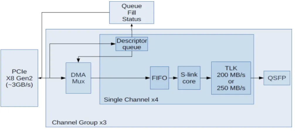
The QuestNP (QNP) card is an S-LINK data source card based on the Common Readout Receiver Card (C-RORC) [33] hardware. It can be used to replay data from the Pixel and SCT detectors. The ability to
replay ATLAS data to the FTK system, as in a data-taking run, is crucial in order to allow full commissioning during a shutdown and complements data-playback features available in individual FTK boards.
The QNP card is implemented by using a dedicated firmware design reusing elements from the firmware of the RobinNP [20] ROS. The C-RORC is a PCI express card using a Xilinx Virtex-6 FPGA [34] as the main component handling the communication through a PCIe Gen 2 (8 × 5.0 Gb/s) interface and implementing the interfaces to twelve optical links via three Quad Small Form-factor Pluggable (QSFP) transceivers. The QNP card makes it possible for user-defined data to be transferred to remote S-LINK data receivers in parallel on each of the 12 S-LINKs. The QNP card has been successfully used to reliably transmit data to the FTK system at an event rate of 1 kHz and has been used for testing up to 19 kHz. A version of the firmware including a Direct Memory Access (DMA) structure for each of the channels in the card is shown
in Figure3. It has reached a fragment rate corresponding to the 100 kHz required by the FTK system.
Figure 3: Diagram of the QuestNP firmware design used to input test data into the FTK via the QSFP connection.
In a possible final implementation of the firmware, the QNP card would be able to synchronize the event header between its 12 internal channels. A daisy chain of the cards using low-voltage differential signalling (LVDS) pairs routed on the eight-position, eight-contact socket (RJ45 connector following the IEC 60603-7 standard) and a dedicated switch would also allow the synchronization of the output of multiple QNP cards. During Run 2, an event arrival-time difference between data from the Pixel and SCT detectors was observed, and the aforementioned synchronization mechanism would have been used to emulate this skew.
Up to three QNP cards can be installed in a 3U rack-mounted server. Five dedicated servers were used to host the 13 QNP cards used to feed data to half of the FTK system. A state-aware sender application, compatible with the ATLAS Run Control [13], is used to configure and control the cards. Monitoring of the application, of the cards’ parameters and of the sent data is implemented through the Information Service (IS) [35] and the information is displayed using Grafana [36].
3.3 Input Mezzanine
The IM module receives and processes data from the inner detector. Each input channel, fed by an inner detector readout link, is processed independently of the others and propagated to the DF. The IM forms
inner detector hits into contiguous clusters and computes their centroid positions. SCT data split at the ABCD [37] front-end readout chip boundary are merged into a single cluster.
The key performance requirement for the IM is maintaining Pixel clustering throughput at the full rate of incoming data. In order to achieve this goal, the firmware is built with parallel clustering cores fed with a load balancing mechanism. Pixel clustering reduces the data size by a factor of 2–2.5. Simulation with Pixel data has shown that four cores are needed to achieve the required processing rate. This performance was demonstrated using simulated data with a pile-up of 80 before the boards went into production, as reported in Ref. [38]. The implemented firmware instantiates eight cores, allowing for an additional safety margin. Bit-level simulations and debugging were performed by comparing bit-by-bit the Pixel clusters from the IM with those produced within the FTK simulation in order to reach per-bit agreement.
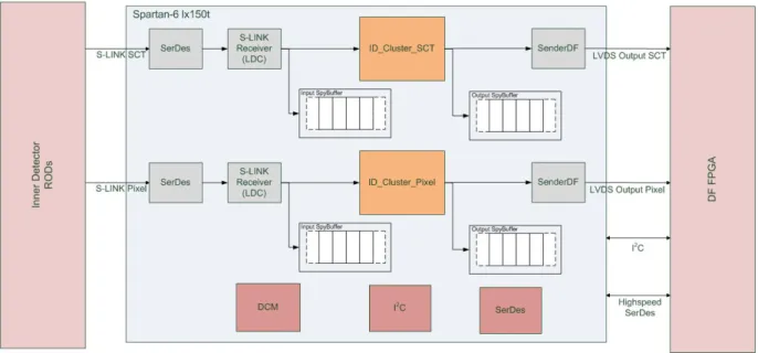
Each IM receives data from four readout fibres using S-LINK. The fibres are distributed to two FPGAs,
two links per FPGA, with the output sent to the DF over a parallel DDR LVDS bus, shown in Figure4.
The ID_Cluster_SCT and ID_Cluster_Pixel are the two main blocks performing SCT and Pixel clustering respectively. The Serializer–Deserializer (SerDes) plus S-LINK blocks receive data from the inner detector
RODs. The SenderDF converts data to LVDS DDR output for the DF. The I2C protocol is used for
configuration. An additional SerDes per FPGA is connected to the DF FPGA as a spare 2 Gb/s line. Each FPGA is also connected to an external RAM that can be used to store test data for IM and system testing purposes. The firmware is modular, which allows different versions of the firmware to be compiled, allocating one FPGA for SCT–SCT, or SCT–Pixel, or Pixel–Pixel processing.
Figure 4: Top-level diagram for each of the two FPGAs on the Input Mezzanine card. The ID_Cluster_SCT and ID_Cluster_Pixel are the two main blocks performing SCT and Pixel clustering respectively. Data flows from the inner detector RODs to the Data Formatter FPGA.
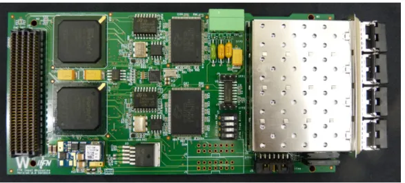
Two versions of the IM cards were produced. The first version is based on the Spartan-6 150T FPGA [39] and is shown in Figure5. It was tuned for Pixel processing during the initial design. The addition of the IBL required a more powerful FPGA, because the effective input hit rate increased by a factor of 2–2.5. The second half of the production used an updated design with Artix-7 200T FPGAs [40] to provide additional processing power.
Figure 5: Photo of the Spartan-6 Input Mezzanine card, component side.
The full FTK system requires 128 IMs installed on 32 DFs. This allows for up to 256 Pixel+IBL input links and up to 256 SCT input links. The 256 inputs for Pixel+IBL exceed the design requirements in Ref. [1] and were sufficient to cover increases in the number of Pixel links during Run 2, which were used to achieve higher Pixel output bandwidth. A small additional production of IMs was planned for the LHC LS2 to provide the required connectivity in Run 3.
The Pixel clustering logic is organized into three main blocks, as shown in Figure6: Hit Decoder, Grid
Clustering and Centroid Calculation. The Hit Decoder block performs the decoding of incoming data. As a part of decoding, it duplicates hits from the ganged region (merged pixels near the edges) of the Pixel module to avoid an efficiency loss in that area. It also rearranges data that arrive from the 16 front-end ASICs of a single Pixel module so that the data are approximately sorted in increasing column order for the grid of pixels in the module. The Pixel module is read out in pairs of columns. For the eight front-end ASICs on one side of the Pixel module, the columns are read out in increasing order, while for the other side the readout is by decreasing order. The described firmware block reorders the column pairs to have the same order. As described in Ref. [38], this is required by the next block, Grid Clustering, described below. Finally, the Centroid Calculation block receives Pixel hits grouped into clusters, calculates the cluster centroid and outputs a single word with the centroid coordinates local to the module and the cluster size projected in two dimensions. This word is the cluster position that is used by the rest of the FTK system for processing.
The IM input logic also allows selective processing of events, by stripping out cluster words, based on the L1 trigger that fired the event and a versatile prescale function. These features are useful for controlling which trigger streams are processed and to control the processing load in the FTK system. For example, it could be used to restrict FTK processing to events where full tracking is required, e.g. those with jets and 𝐸Tmiss. The prescale has the functionality to send every 𝑛thevent full or empty, which is useful for debugging problems that only occur in successive events.
The Grid Clustering is the most resource-intensive block of the firmware. It processes incoming data to find hits that are contiguous along horizontal, vertical or diagonal lines. This operation is performed using a grid that represents an 8 × 21 portion of the Pixel detector. The grid is aligned to the first hit received, called the seed, and loaded with all other hits present. This grid, replicated in the FPGA, uses local logic to
select hit pixels that are contiguous to the seed, or contiguous to selected pixels. In this way, all pixels of the cluster containing the seed are selected. The readout logic then extracts all selected pixels. The output is the sequence of all hits of the clusters, with the last hit identified by an end-of-cluster flag. Next, iterative processing is done to cluster the data present on the grid but not belonging to the seeded cluster.
The logic is organized into parallel cores as described in Figure6. The baseline Pixel clustering firmware instantiates eight parallel engines. Data received from the Hit Decoder block is organized into a sequence of detector modules for each event. For load balancing, the Parallel Distributor assigns data for an entire module to the engine with the smallest load as informed by the Engine Minimum block. Each of the eight parallel engines has enough buffering to compensate for fluctuations in the processing time without causing a significant number of control signals to be sent upstream. Each of these eight parallel engines works in a first-in first-out (FIFO) mode, thus preserving the order in which data blocks flow. A parallel FIFO stores the event identifier which is sent for each data block from the Pixel and SCT detectors. This event identifier is used by the Data Merger at the right side of the diagram to collect the correct data, for a given input S-LINK, for each event from the engines before sending the built event to the DF. The output data are organized into module packets with each packet corresponding to the data from a single Pixel or SCT module. For most of the tests reported in this paper, the output packet size was limited to 32 words including one header and one trailer word. The words are 32 bits long. In the body of the packet, 𝜂 and
𝜙hit-coordinate pairs correspond to one 32-bit word. The IM works independently on data from each
S-LINK. Synchronization of data from different S-LINK inputs is performed in the DF.
Figure 6: Diagram showing the organization into parallel engines for the Pixel clustering logic. This logic is organized into three main blocks: Hit Decoder, Grid Clustering, and Centroid Calculation.
The firmware used for tests reported here in the Spartan-6 FPGA to handle SCT–Pixel processing with two parallel clustering cores utilized approximately 56% of the logic and 71% of the memory. The equivalent firmware on the Artix-7 FPGA with eight parallel clustering cores utilizes approximately 71% of the logic and 31% of the memory.
3.4 Data Formatter
The DF receives packets of hits from the IMs and other DFs and routes them to downstream boards, sorted by towers, or to other DFs. Its main task is to assign all module data to the appropriate towers, duplicating
data where necessary. The DF is based on the Pulsar [41,42] ATCA board with full mesh connectivity via
the backplane to up to ten other modules in the ATCA shelf over dual duplex multi-gigabit-transceiver connections. In addition to the connections to the ATCA backplane, the DF has connections to an RTM that hosts ten QSFP ports that provide up to 40 duplex connections. The DF hosts four mezzanine cards which can transmit data to the DF via LVDS lines. The switching functionality in the DF is performed using a Xilinx Virtex-7 690T FPGA [40]. In the DF application, the Pulsar board uses an Intelligent Platform Management Controller (IPMC) for some module control functions.
IM
16 S-LINK inputs
1.28 Gb/s 8ouputsper AUXsorted by layer
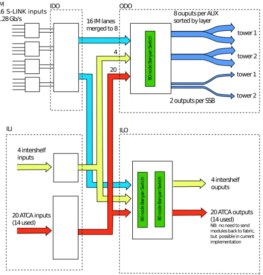
2 outputs per SSB tower 1 tower 2 tower 1 tower 2 20 ATCA inputs (14 used) 4 intershelf inputs 4 intershelf ouputs 20 ATCA outputs (14 used) NB: no need to send modules back to fabric, but possible in current implementation 16 IM lanes merged to 8 IDO ODO ILO ILI 4 20 80 n od e Ba ny an S w tic h 80 n od e Ba ny an S w tic h 80 n od e Ba ny an S w tic h
Figure 7: Diagram of dataflow in the Data Formatter firmware design. Clustered hit data from the Input Mezzanines are sent to downstream boards via the Output Data Operator (ODO) block or are shared with other Data Formatters via the Internal Link Output (ILO) block.
IM transmits two lanes of hit data over six-bit DDR links operating with a clock speed of 200 MHz. In each clock cycle the DF receives eight data bits, three control bits and one parity bit giving a data transfer rate for each lane of 1.6 Gb/s.
As mentioned in the previous section, module packets from the Pixel and SCT detectors consist of a header, a trailer, and coordinate hits in 32-bit words. The DF switches and duplicates these module packets and does not alter their content. As can be seen in Figure7, data from the IM are received in the DF firmware module called the Input Data Operator (IDO). The IDO detects L1 ID mismatches among the 16 IM inputs and discards inputs with corrupted L1 IDs.
If a module packet has a destination in the tower hosted by the current DF board it is copied into one of eight lanes which are transmitted to the Output Data Operator (ODO) switch via 32-bit-wide FIFO buffers. If a module packet has a destination hosted by another DF board, it is copied into one of a separate set of eight lanes which are transmitted to the Internal Link Output (ILO). It should be noted that the IDO will send some module packets via both connections.
Module data packets from other DF boards are received using 8b10b encoding by the Internal Link Input (ILI). Module data packets from other DF modules in the same shelf are received over the ATCA backplane. Module data packets from other ATCA shelves are received via optical fibres. The data speed for the payload on a single fibre or backplane connection is approximately 5 Gb/s for both backplane and fibre transmission. For both the backplane and fibre connections, there are pairs of duplex fibres, giving a total bandwidth between DF boards, in each direction, of approximately 10 Gb/s.
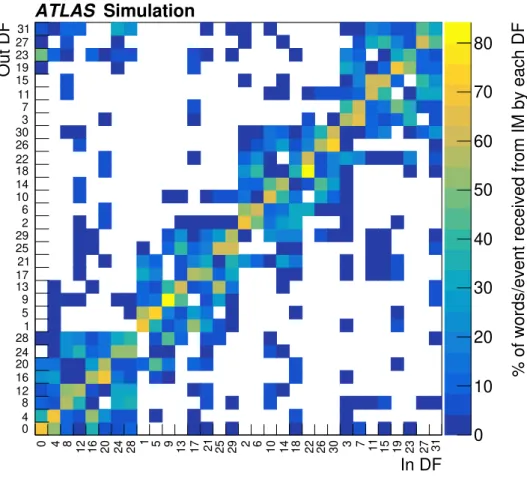
Figure8shows the fraction of data from the IMs of one ‘In DF’ that is sent to various DFs in the system. Typically, 60% or more of the input data from the IM modules is used by the DF that hosts the IM modules. The rate of data shared with other DFs corresponds to the off-diagonal elements in the figure. The amount of data which must be shared with other ATCA shelves is much smaller than the amount of data which remains in a given ATCA crate. Given the constraints inherent in the Pixel and SCT readout, the cabling was optimized to reduce data sharing between the DF boards and between ATCA shelves. A worst-case scenario of 𝑡 ¯𝑡 Monte Carlo simulation with at least one leptonic-decay at high pile-up was used to generate the plot in Figure8.
The ILO receives module data packets from the IM cards via the IDO and also receives data from other DF modules for transmission over the backplane or fibres connecting the DFs to different shelves via the ILI. This allows any given module data packet to be routed to any of the 32 DFs in the system. The routing tables and layout of the system were configured to minimize the number of instances in which a module packet requires several hops over fibres and backplanes to reach its final destination. The minimal extra bandwidth needed by these rare extra hops is not reflected in Figure8.
The ODO receives module data packets from the IDO and the ILI. This block is responsible for sending data to the downstream boards, out of the DF system. Module data packets needed by the AUX and SSB are sorted into two towers of eight and four layers each, respectively. Module data packets needed by the SSB are transmitted directly to the SSB. If a given module data packet is needed by more than one tower it will be duplicated by the switch in the IDO.
The data switching in both the ODO and ILO is performed using a Banyan switching network which consists of 16 × 5 nodes allowing each input module data packet to be switched to one or more of the 32
output nodes. Each node (see Figure9) consists of two buffered inputs and intermediate memory large
enough to store the largest module data packets produced by the IM. The nodes can switch packets to the output nodes according to a 32-bit address mask and duplicate the packet as required by the address mask.
In DF 0 4 8 12 16 20 24 28 1 5 9 13 17 21 25 29 2 6 10 14 18 22 26 30 3 7 11 15 19 23 27 31 Out DF 0 4 8 12 16 20 24 281 5 9 13 17 21 25 29 2 6 10 14 18 22 26 30 3 7 11 15 19 23 27 31
% of words/event received from IM by each DF
0 10 20 30 40 50 60 70 80 Simulation ATLAS
Figure 8: Fraction of input Input Mezzanine module (hosted by Data Formatters labelled ‘In DF’) data shared with other Data Formatter boards (labelled ‘Out DF’) for distribution to Auxiliary Cards and Second Stage Boards. Data whose destination is within the same shelf are shared over the ACTA backplane. The board numbers in the figure are arranged in blocks of eight corresponding to one ATCA shelf each. Sharing of data with other Data Formatter shelves requires at least one hop on an optical fibre.
Figure 9: A single node in the Banyan switch showing input buffers and intermediate buffers. The buffers are 32 bits wide.
The Banyan switching network was simulated using a Unified Verification Method (UVM) simulation and it was demonstrated that the network could handle the expected Run 3 FTK load at the full 100 kHz input rate.
The firmware used in the Virtex-7 690T FPGA on the Pulsar board for the tests reported here uses approximately 78% of the logic lookup tables, 49% of the flip-flops and 70% of the block RAM.
3.5 Auxiliary Card
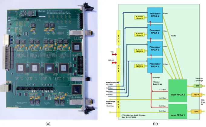
The AUX transports hit data to the AMB and evaluates the returned track candidates, before sending candidates which pass the selection requirement to the SSB. Each of the 128 PUs is composed of an AUX and AMB pair. The AUX is a 9U VME RTM that is 280 mm deep. It communicates via a P3 connector with the AMB and with the DF and SSB via QSFP connections.
The AUX contains six Altera Aria-V GX FPGAs [43], two FB7H4 for input/output and four FB5H4 processing chips. Each processing chip is connected to one of the AMB Little Associative Memory Boards
(LAMBs). The AUX board is shown in Figure10(a)and the dataflow is sketched in Figure10(b). Clusters
from eight silicon detector layers are sent from DF boards to the AUX via a QSFP connection; the Input-1 FPGA receives data from three Pixel layers and one SCT layer, while the Input-2 FPGA receives data from the other four SCT layers. Coarse resolution hits, called SuperStrips (SSs), are sent to the AMB for pattern recognition over 12 × 2 Gb/s lines through the P3 connector. Both the SSs and full resolution hits are sent to the processor chips. The processors also receive from the AMB the addresses of roads (matched SS patterns) that have hits on at least seven of the silicon detector layers over 16 × 2 Gb/s lines back through the P3 connector. For each of those roads, the Data Organizer (DO) portion of a processor FPGA retrieves all of the full resolution hits in the road. The Track Fitter (TF) portion then fits each track candidate (each combination of one hit per layer) and calculates the 𝜒2. Those tracks passing a 𝜒2cut are sent to the Input-2 FPGA where the four processor streams are synchronized and duplicate-track removal is performed before the remaining tracks are sent to an SSB via S-LINK over a Small Form-factor Pluggable (SFP) connection. All of the data processing is completely pipelined using local control signals for dataflow control.
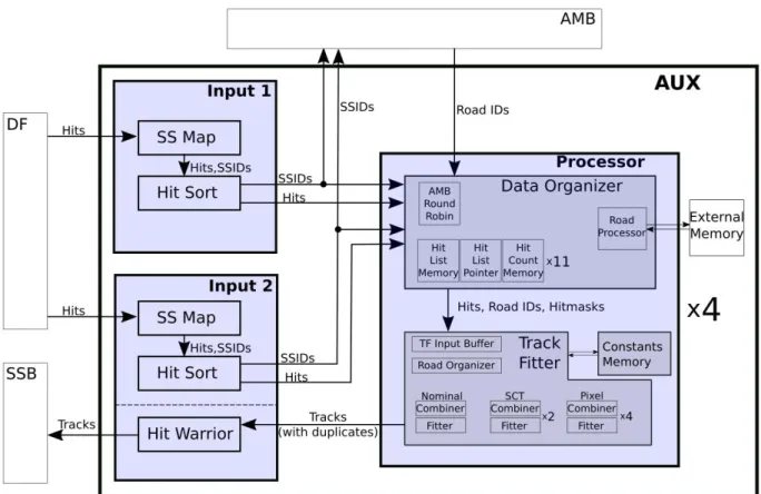
An overview of the AUX firmware is shown in Figure11. Hits from the DF enter the SS Map in which the
32-bit hit word is converted to a 16-bit SS using lookup tables. The Hit Sort module uses a base-4 radix sort to guarantee that all hits in the same SS are sent out sequentially. Each SS is sent to the AMB while the SS plus full resolution hit (a combined 48-bit word) is sent to all four processor chips.
There are two major functions in a Processor FPGA, the DO and the TF. The DO receives roads from one of the AMB LAMBs on four serial links and uses a round robin to process them with minimum latency. The hits from the eight detector layers are processed in parallel. The DO is a database built on the fly for rapid retrieval of all hits in a road. Three sets of memory are used: the Hit List Memory (HLM) stores each hit sequentially as it arrives; the Hit List Pointer contains a pointer to the first HLM location for each SS; and the Hit Count Memory contains the number of hits in the SS. These databases are replicated for each of the 11 coordinates used in Eq.1, as shown in Fig.11. There are two copies of the DO which act as a ping-pong buffer. At any instant one is in Write mode, filling the memories with the data for event 𝑁 , while the other is in Read mode, retrieving hits in roads for event 𝑁 − 1. For each road, the data sent from the DO to the TF consist of the road number, all of the full resolution hits in the road, and a hit mask noting which layers have hits.
(a) (b)
Figure 10: The (a) physical Auxiliary Card and (b) dataflow through the Auxiliary Card, starting from the lower-right.
The TF block fits each track candidate using a linear approximation and prestored constants, as described in Section2and Eq. (1). In the AUX, only the 𝜒2is calculated. For each road received from the AMB, the Road Organizer stores the road and hits and initiates the fetching of the fit constants from memory. The data and constants are then sent to the appropriate fitter where each combination of one hit per layer is fit and its 𝜒2tested. The tracks that pass the test are sent to the Hit Warrior (HW) in the Input-2 FPGA, which does duplicate-track removal. If two tracks share more than a programmable number of hits, the one with the lower 𝜒2is retained.
There are three types of fitters: the SCT Majority Fitter, the Pixel Majority Fitter, and the Nominal Fitter. The Majority Fitters allow one missing hit from their respective detectors to improve the track-finding efficiency. For the Nominal Fitter, in parallel with the full fit, eight Recovery Fits are done in which one of the hits is dropped. If the full fit fails the 𝜒2cut but a recovery fit passes the cut, that fit is retained because it is assumed that a good track had a missing hit, but a random hit landed in the dropped layer. Based on analysis of simulated data, the optimal use of FPGA resources are one, two, and four implemented Nominal, SCT Majority, and Pixel Majority fitters respectively. These fitters operate in parallel.
The firmware in the AUX FPGAs used for the tests here, including monitoring and error handling, came close to saturating the available resources. For the processor chips, > 70% of the logic and 75% of the memory are used. For the input FPGAs, about 40% of the logic and > 80% of the memory are utilized.
Figure 11: Diagram of the Auxiliary Card firmware design.
3.6 Associative Memory Board
The AMB [25], shown in Figure12is the part of the PU that is devoted to pattern matching between the
SSs sent by the AUX and the patterns simulated for each 8-layer road. This functionality is implemented
through a custom ASIC: the AM06 described in Section3.7.
An AMB consists of a 9U-VME mainboard and four identical mezzanines, the LAMBs. Four FPGAs are installed on the mainboard: two Xilinx Spartan-6 (45T and 16) [39], which control the VME interface and the state of the board respectively; and two Xilinx Artix-7 200T [40], which control the input and output logic. Each LAMB is equipped with 16 AM chips and a Xilinx Spartan-6 FPGA, dedicated to the configuration and monitoring of the mezzanine.
The AUX and AMB are connected through the VME P3 connector, as shown in Figure13. High-speed
serial links provide 12 Gb/s as input from the AUX to the AMB and 16 Gb/s as output from the AMB to the AUX. The SSs provided by the AUX are received by the Xilinx Artix-7 FPGA handling the input, called Hit. This FPGA sends a copy of the SSs to each of the four LAMB mezzanines installed on the AMB. Two sets of eight 1-to-2 fan-out buffers (one per input link) distribute the same data to all the LAMB mezzanines. The Hit FPGA buffers the data and synchronizes the inputs by sending a new event only when all the mezzanines have finished processing the previous one.
On the LAMB, the SSs are distributed to the AM chips. A chain of 1-to-4 fan-out buffers in cascade allows each AM chip to get a copy of the SSs. All of the selected roads are sent to the Xilinx Artix-7 FPGA
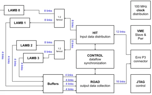
Figure 12: Photo of an Associative Memory Board with four LAMBs mounted. Additional LAMBs can be seen in the background. 100 MHz clock distribution VME Slave & Pwr Erni P3 connector JTAG control HIT
Input data distribution
CONTROL
dataflow synchronization
ROAD
output data collection
1:2 fanout 1:2 fanout LAMB 0 LAMB 1 LAMB 2 LAMB 3 Buffers 8 links 8 links 8 links 8 links 8 links 8 links 4 links 4 links 4 links 4 links 4 links 4 links 4 links 4 links 16 links 12 links
Figure 13: Block diagram of the Associative Memory Board (AMB) structure. The black arrows show the dataflow in the AMB.
handling the output, called Road. This FPGA collects all the roads belonging to the same event before sending them to the AUX for the 8-layer fits described in the previous section. A dedicated Spartan-6 FPGA, named Control, controls the dataflow on the board and synchronizes the Hit FPGA and Road FPGA.
A fourth Spartan-6 FPGA, named VME, handles the communication on the VME bus and takes care of the board configuration and monitoring.
An AMB is able to load ∼ 8 · 106independent patterns and to perform pattern comparisons at a rate of
∼ 12 petabytes/s, with a peak power consumption below 250 W. The entire FTK system contains 128 AMB, and it includes more than one billion (1 098 907 648) track patterns. A collection of patterns is referred to as a pattern bank.
During the tests performed in 2018, the AMB demonstrated the ability to process events at a rate greater than 100 kHz. Dedicated high-power tests [28] confirmed the designed power consumption of the AMB, and the ability of the custom cooling system, described in Section3.1, to keep the boards within temperature bounds while in the intended Run 3 configuration.
The firmware used in tests reported here for the Hit, Control, and LAMB FPGAs uses up to 50%, 60%, and 45% of the logic resources respectively. The firmware for the Road FPGA uses approximately 30% and 50% of the logic and memory resources respectively.
3.7 Associative Memory
The AM ASIC is a highly parallel processor for pattern matching, hosted on mezzanines on an AMB, which feeds in SuperStrips and reads out roads. The AM ASIC used by the FTK system, the AM06 [18] shown in
Figure14, is designed in 65 nm CMOS technology. The design of the AM chip combines full-custom
content-addressable memory arrays, standard logic cells and SerDes IP blocks at 2 Gb/s for input/output communication. The AM chip is able to perform pattern matching in parallel on all the 131 072 patterns stored on its 168 mm2die. The stored patterns are composed of a set of eight SSs, one for each detector layer used by the FTK. The 16 bits of each SS are stored on 18 XORAM [44] cells forming an AM cell. The XORAM cell is composed of a conventional six-transistor SRAM cell, which stores the data, merged with an XOR gate executing the matching with the input at a clock rate of 100 MHz. Two XORAM cells can be paired to allow the presence of ternary bits in the pattern to be stored. When two XORAM cells are used to store the value of a single bit, the bit-value can assume three values “0” (or ‘00’), “1” (or ‘11’), and “𝑋” (either ‘01’ or ‘10’). While for the “0” and “1” values the pattern behaves as if no ternary bit is present, the “𝑋” value can be used as a Don’t Care (DC) value. The DC bits are bits in the pattern that are always considered matched, regardless of the value of the corresponding bits in the input word. Effectively, these DC bits increase the width of the pattern by a factor of 2𝑁𝑋
, where 𝑁𝑋 is the number of DC bits used
in a pattern. This provides variable resolution patterns, allowing some patterns to be wider than others. Figure1uses a dotted line as a visual representation of this on the second layer. While the configuration used by the FTK uses a 16-bit SS with up to two DC bits, the AM chip can be configured to accommodate from two to nine DC bits for each pattern. The XORAM cell is optimized to achieve a power consumption of 1 fJ/bit-comparison, allowing 64 AM06 to be installed on a single VME board.
As shown in Figure15, SSs are received by the AM06 asynchronously on the eight input serial-buses. The
SSs are deserialized and transmitted in parallel to the FILTER module that takes care of correctly encoding ternary bits by mapping the 16-bit input words to 18-bit words. This module can also receive data through
Figure 14: Photo of the bottom (centre) and top (right) of the AM06. On the left a 1-euro coin is shown for size comparison.
the JTAG connection in order to write the pattern data and to test the stored pattern. The 8 × 18-bit data are propagated to all of the memory locations in the chip where they are compared to the stored pattern. The match status for each of the eight layers in a pattern is held until all the data belonging to the same event are received. At the end of the event, a majority block counts the number of matched layers for each pattern. If the number of matched layers is greater than a selectable threshold, the pattern identifier is sent to the PATT FLUX module. This module adds a chip geographical address to the internal pattern address and handles the chip output. Patterns received from previous chips in the daisy chain are deserialized and sent to the PATT FLUX module, which buffers the data and ensures they are transmitted before the given chip’s data. The end of an event resets all of the AM cells in the ASIC so that the AM chip can process data belonging to a new event while sending out the matched patterns.
DESERIALISER BLOCK FILTER BUS 0 (lvds) BUS 1(lvds) BUS 2(lvds) BUS 3 (lvds) BUS 4 (lvds) BUS 5 (lvds) BUS 6 (lvds) BUS 7(lvds) BUS <0..7> [0..15]
PATTERN BANK MAJORITY
BUS <0..7> [0..17] JT AG TCK TMS TDI TDO DESERIALISER DESERIALISER PATIN 0 (lvds) PATIN 1 (lvds) SERIALISER PATT FLUX addr_out [0..31] Test_mode Jpat_data [0..143] Write_en Write Op_code Set_Threshold Geographical_address Request_layermap PATOUT (lvds)
Figure 15: Diagram of the dataflow through the AM06 chip.
The AM chips can be connected in a daisy chain to maximize the number of stored patterns on each AMB while maintaining a simple routing at the board level. Two dedicated inputs are present on each AM06 to receive data from previous AM chips in the chain. The pattern identifiers collected on the two inputs are copied to the AM chip output.
To allow the full system of 128 PUs to be commissioned, more than 9000 AM06 were produced in two production rounds. A first batch of 2159 preproduction chips, including slow corner and fast corner chips,2 was delivered in 2014 and tested in-house, achieving an estimated yield of 83% for the slow corner and 89% for the fast corner. The production batch composed of 8126 ASICs was delivered in 2016 and tested by an external company. The average yield for the production batch was 83%. AM chips from this batch were split into two groups. Normal chips are required to pass all functional tests at nominal power consumption and clock speed. High-performance chips are those which pass all functional tests with a 10% increase in clock frequency and 5% decrease in voltage. High-performance chips account for roughly 65% of the produced AM chips, and normal-performance chips account for roughly 15% of the produced AM chips. A correlation of the yield with the mechanical wear of the AM chip socket was observed, with more chips ending up in the lower performance group. Only high-performance chips were expected to be mounted on the production boards. Retesting of chips to recover more of them was planned after having understood the effect of the aging of the test-stand.
3.8 Second Stage Board
The SSB receives 8-layer tracks from the AUXs and clustered hits from the DF on the four layers that are unused in the pattern matching. It extrapolates these tracks into the four layers to search for hits, performs 12-layer track fits and removes duplicate tracks before outputting the final FTK tracks. A full track packet consists of its helix parameters, 𝜒2value, and associated cluster coordinates. A schematic description of
this functionality and the dataflow through the SSB is shown in Figure16. The second-stage processing
hardware consists of a VME main board and RTM, shown in Figure17.
Second Stage Board
Hits from additional four layers from
Data Formatter
8-Layer tracks from four AUX cards
Output to FLIC/ROS SFP Hits Hits Hits 12-Layer Tracks 8L Tracks 8L Tracks 8L Tracks Ext. Memory Track Fitter 12-layer track fitting
EXTF FPGA Extrapolator Extrapolate 8-layer track to SSs on extra 4 layers EXTF FPGA
Hit Warrior FPGA
Data merging and track duplicate removal EXTF FPGA EXTF FPGA QSFP SFP x4
Figure 16: Diagram of the dataflow through the Second Stage Board.
2The fast corner and slow corner chips are obtained with a variation of fabrication parameters that are optimized for set-up
and hold time respectively. This has the effect of producing chips that on average will work at slightly faster or slower clock frequencies.
!
Figure 17: The physical RTM (left) and MAIN Second Stage Boards (right).
The processing of hits and tracks is performed on the SSB main board (SSB MAIN), which hosts six Xilinx Kintex-7 FPGAs [40] (four 410T-FBG900 and two 410T-FBG676). Four of the FPGAs, Extrapolator and Track Fitters (EXTFs), perform the extrapolation and 12-layer track fitting. One FPGA, the Hit Warrior (HW), merges the streams, performs duplicate-track removal, and sends final tracks to the FLIC or ROS. The remaining FPGA provides the VME interface. The high-speed serial interfaces to the DF, AUX cards, and FLIC are provided by the SSB RTM, which also has serial interfaces to other SSBs intended for duplicate-track removal. Data arrive at the SSB from a DF via a QSFP connection and from AUXs via SFP connections. Two of the QSFP channels and two SFP connections are routed to each of the two ‘primary’ EXTFs, those that are directly connected to the input data streams.
Each EXTF FPGA has three main functions. First, the EXTF synchronizes the data streams from up to two AUXs and one DF covering one FTK tower. Second, 8-layer track information is used to extrapolate the track into SSs on the additional IBL and three SCT layers. The SSs of the most likely hit positions are then retrieved. Last, the clustered hits in the extrapolated SSs are retrieved and combined with the 8-layer track hits to perform full 12-layer track fits, as described in Section2and Eq. (2).
Tracks are required to pass a 𝜒2selection before being sent to the HW FPGA. Up to one hit in the additional four layers is allowed to be missing or dropped in a recovery fit as in Section3.5. When using all four EXTFs on the board, two of the EXTFs each receive their input data via pass-through from one of the primary EXTFs. Configuration and monitoring data are read in and out through the VME interface. The
firmware design is illustrated in Figure18. Up to 80% of the logic resources and 90% of the memory of
the FPGA are used in the design.
Constants for extrapolation and track fitting are stored on external RLDRAM, accessed with a 400 MHz DDR clock. Two chips per EXTF, with memory totalling 576 Mb, are available for the extrapolation constants, and four chips per EXTF, totalling 1152 Mb, are available for the track-fitting constants. The HW FPGA has two primary functions on the SSB. First, the HW combines the event data streams from up to four EXTF FPGAs. Second, it searches for and removes any duplicate tracks from the combined data stream and outputs the filtered event data stream to either the ROS or FLIC. In addition to its primary functions, the HW also provides monitoring and histogramming of output track parameters. As in the
Figure 18: Block diagrams of the firmware in the Extrapolator and Track Fitter (EXTF) FPGA on the Second Stage Board split into the Extrapolator (top) and Track Fitter (bottom) firmware design. The AUX and DF wrappers receive the 8-layer track and additional hits respectively. The Extrapolator’s output manager feeds into the Track Fitter’s Road Organizer, and the Track Fitter sends tracks to the Hit Warrior via the Event Wrapper.
EXTF FPGA, these monitoring data are read out over the VME interface. A top-level block diagram for the firmware is shown in Figure19.
Hit Warrior Top Level
VME interface Sync Engine SpyBuffers Freeze Handler GTX to FLIC LVDS from EXTF 1 LVDS from EXTF 2 LVDS from EXTF 0 LVDS from EXTF 3 Hit Warrior Histograms
Clock Reset Engine Clock Reset EngineClock Reset Engine
Figure 19: Diagram of the Hit Warrior firmware design for the Second Stage Board.
Data arrive from each EXTF FPGA over a parallel LVDS interface operating at 180 MHz. The input logic extracts the event packets and presents them to a multiplexer called the Sync Engine. The Sync Engine combines the event packets pertaining to the same event identifier. The HW track filter algorithm is then applied. This algorithm writes the data into a FIFO, not shown in Figure19. As the data are written into the FIFO, each track is compared with all previous known tracks for this event. Any detected match is marked. Tracks are considered to be duplicated if the tracks come from the same sector and they have the same hit coordinates for at least eight layers. If a duplicate is found, the track with more hits is kept. If both tracks contain the same number of hits, the track with a smaller 𝜒2value is kept.
When the HW algorithm FIFO is read out, any duplicate-track data are removed such that the data leaving the HW only contains unique tracks. These output tracks are formatted to be sent to either the ROS or FLIC. The final version of the HW firmware can handle an average of 141 tracks per SSB at an event rate of 100 kHz. After duplicate-track removal, the HW is able to maintain an average output event size of 28 tracks per SSB at 100 kHz. Up to 20% of the logic resources and memory are used in the FPGA design. The full FTK system requires 32 SSB MAIN and 32 SSB RTM boards. By the beginning of spring 2019, the required production boards were fully tested for integration at CERN and by the beginning of summer 2019, three additional spare SSB MAIN boards and five additional spare SSB MAIN boards were at CERN.
3.9 FTK-to-High-Level-Trigger Interface Card
The FLIC is a custom ATCA card that interfaces the upstream FTK components with the HLT. The FLIC boards receive tracks via the eight 2 Gb/s optical links on the front panel, which are connected to the SSBs. The key functionality of the FLIC is to find and insert the global module IDs into the output by using lookup tables. These are used by the HLT to obtain global coordinates from the local FTK coordinates. In
addition, the output packet is formatted to the standard ATLAS event format before it is sent to the HLT farm. This final packet includes an error word to inform the HLT of possible problems with the contents of the output packet. Besides data processing, the FLIC sends data over the backplane to multiple processor blades mounted in the same ATCA shelf in order to perform data quality monitoring.
Figure 20: The FTK-to-High-Level-Trigger Interface Card (left) and its RTM (right).
There are two FLIC boards in the FTK system, hosted in the hub slots of the ATCA shelf, and two processor blades hosted in the payload slots. Event packets can be sent to any of the processor blades via 10 Gb/s
Ethernet. The FLIC board consists of the input card and the RTM, shown in Figure20. The input card
has two areas, the data processing area and the management area. Four Xilinx Spartan-6 75T-FGG676 FPGAs [39] are installed in the data processing area. Two of them handle the data processing and the other two communicate with the processor blades over the ATCA backplane. The first two are referred to as the processing FPGAs while the other two are referred to as the interface FPGAs. The four FPGAs are connected to each other via a full internal mesh of high-speed LVDS lines with a designed bandwidth of
4 Gb/s, shown in Figure21.
The management area provides slow control and monitoring of the FLIC board. One small Spartan-3 S400-FG320 FPGA [45], one Microchip Peripheral Interface Controller (PIC), four Flash RAMs, and one IPMC card are located in the management area. The Spartan-3 FPGA provides level translation and bus control logic to interface the microprocessor and Flash RAMs to the Spartan-6 FPGAs. The firmware and lookup tables are stored in the Flash RAM. Commands are sent through the front-panel Ethernet port to the PIC to perform register and data accesses to all other devices by controlling the small FPGA. All monitoring information can be transferred through the IPMC to the shelf manager.
Data processing in each processing FPGA has four pipelines. Each pipeline receives data from one SFP connection on the front panel and processes the data. The core data processing functionality, ATLAS global module ID lookup, is performed with the help of 32 Mb of fast SRAM per input link. Each track header has the address for the lookup embedded so that the lookup can be initialized immediately after the track starts being processed. The lookup and track processing are done in parallel to ensure the module IDs are ready to be inserted when the track processing finishes. The merge state machine combines the module IDs and the remaining event packet, formatted in the ATLAS event format. The packets are then sent out from the RTM to the HLT over eight fibres using 2 Gb/s S-LINKs. The data processing pipeline is
Spartan-6 ATCA Interface FPGA U3 Spartan-6 data processing FPGA U1 Spartan-6 data processing FPGA U2 Spartan-6 ATCA Interface FPGA U4 To fabric To fabric To fabric To fabric SFP Inputs To RTM SFP Inputs To RTM
Figure 21: Diagram of the connections including the internal mesh connecting each FTK-to-High-Level-Trigger Interface Card FPGA to the others with four high-speed GTX lines.
version of the firmware that emulates the output of the upstream FTK system can be loaded to either or both of the processing FPGAs. FPGAs with the nominal firmware loaded can receive emulated event packets to perform a loop-back test.
Figure 22: Diagram of the data processing pipeline in the FTK-to-High-Level-Trigger Interface Card processing FPGA. The input lines (left) receive data from the Second Stage Boards.
The FLIC also implements higher-level monitoring functionality where the two interface FPGAs copy selected fragments from the processing FPGAs via the internal mesh. Those fragments are then assembled by using the event identifier and sent to the processor blades using Ethernet. Each pipeline only receives information from a part of the FTK system, while the assembled fragments contain information for the whole system, allowing advanced event-level monitoring.
4 Online software, control and monitoring
The FTK online software integrates the FTK system into the ATLAS trigger and data-taking infrastructure. It provides features to configure, run and monitor the FTK boards from the ATLAS Run Control (RC) infrastructure, and handle the internal commands and synchronization operations.
4.1 Run Control integration
The ATLAS RC is based on a finite-state machine (FSM) guiding the entire ATLAS detector through standby, configuration, and running states. This general behaviour is inherited by the FTK online software. The FTK software required a dedicated redesign and extension of the ATLAS FSM in order to handle the special cases of the FTK system. For example, it takes about 50 minutes to configure and load the pattern banks into the 16 PUs in one VME crate, which exceeds the time allotted to configure the ATLAS detector. The long configuration time is driven by the need to transfer about 500 MB/board with limited bandwidth and CPU resources. This step was optimized to maximize the usage of the resources on the single-board computer in the VME crate and throughput over the VME backplane. To accommodate this, two configuration transitions were implemented. During the LHC inter-fill, pattern banks and fit constants are loaded onto the boards. During data-taking, only pattern-bank and fit-constant checksums are computed for validation. If a checksum validation failure occurs, the FTK software prevents the FSM transition from completing successfully.
The complexity of operations performed by the FTK boards for different transitions required the development of a multi-threaded approach in order to fit within the ATLAS transition time windows. This is particularly crucial for the AMBs, AUXs, and SSBs hosted in VME crates and controlled by a single-board computer where the bandwidth over the VME bus is a limiting factor. The implemented design provides control of operations per board with options for parallelization, the number of threads, and thread queue management.
Another important aspect of the FTK control software is to handle concurrent access to board resources. In most cases, the firmware does not provide concurrent access management; therefore, access serialization was implemented at the software level by means of mutexes and system semaphores. This approach has the cost of longer delays between operations such as state transitions and monitoring. However, this did not impact data-taking operations.
The software infrastructure allows both the inclusion of the FTK in ATLAS data-taking runs while writing output to the ATLAS data stream and stand-alone parasitic runs writing to an independent data stream. The latter was particularly useful early in the commissioning phase for performing rapid tests, without waiting for an entire LHC fill to retry a test and without negatively affecting ATLAS data-taking. Near the end of Run 2, a vertical slice of FTK was regularly included in ATLAS runs. Using the functionality of the IMs, the FTK system can selectively process events according to the result of the ATLAS L1 trigger. During Run 2 a special trigger was configured to select events with muons that fell within the geometric coverage of the vertical FTK slice that was included in ATLAS data-taking.
4.2 Automated procedures
Two automatic procedures are required for integration into the ATLAS RC framework: Stopless-Removal and Stopless-Recovery. The Stopless-Removal procedure removes a subsystem, or part of it, from the ATLAS FSM when it is interrupting data-taking, without changing the global FSM state. In the FTK software, this was implemented by means of an external application automatically triggered by missing event fragments from the FTK subsystem. This temporary solution proved to be particularly useful during the commissioning phase, where the software infrastructure was rapidly evolving.
Stopless-Recovery consists of a semi-automatic procedure to reinclude components previously excluded from the run, e.g. because of a Stopless-Removal. As implemented in the FTK system, this requires a full reconfiguration of the different boards before reinclusion of the system in the FSM and data-taking. This reconfiguration procedure is managed by an internal ATLAS-like FSM system.
4.3 Monitoring
Another important aspect of the FTK online software is to provide the monitoring functionalities of the board status, on-going operations, and of the quality of the output data. The first is performed by accessing specific board registers and publishing the information to the IS and the Online Histogramming Service (OH) [13]. Additional information is also propagated to higher-level monitoring applications, such as Grafana. Dedicated functions are used to retrieve monitoring information from the boards. Their parallelization can be controlled by assigning them to separate threads or by forcing serialization of the operations. Easy access (e.g. via Grafana) to monitoring information and its history, ranging from basic counters to detailed firmware states, is extremely useful for commissioning, understanding system performance and tracking down bugs in the system.
Data quality information for each board, such as data snapshots and counters, is stored in dedicated spybuffers, which are read out periodically by online software monitoring functions. The data are then published to the ATLAS Event Monitoring (EMON) service by means of a customized interface which provides temporary storage for multiple spybuffers from different boards that can be accessed on-demand for analysis and evaluation.
A freeze mechanism was implemented in order to block the overwriting of the spybuffers when an error occurs and during readout of spybuffers. This functionality was crucial for accelerating firmware debugging and development by catching problematic events in situ.
5 Configuration, optimization and performance
The FTK uses configuration data in the pattern matching and track fitting. The production of this configuration and its optimization are enabled by a functional simulation of the FTK. This simulation of the hardware provides a way to evaluate the performance and validate the output data from the hardware. The FTK technical design report [1] discusses the required tracking efficiencies for several physics cases.
5.1 Simulation
The simulation software for the FTK [46] serves multiple purposes: • support of hardware design decisions,
• production and validation of the input pattern banks, • provision of sectors and constants needed by the hardware, • enabling of new trigger strategies that make use of the FTK,