HAL Id: hal-01745024
https://hal.archives-ouvertes.fr/hal-01745024
Submitted on 9 Apr 2018
HAL is a multi-disciplinary open access
archive for the deposit and dissemination of
sci-entific research documents, whether they are
pub-lished or not. The documents may come from
teaching and research institutions in France or
abroad, or from public or private research centers.
L’archive ouverte pluridisciplinaire HAL, est
destinée au dépôt et à la diffusion de documents
scientifiques de niveau recherche, publiés ou non,
émanant des établissements d’enseignement et de
recherche français ou étrangers, des laboratoires
publics ou privés.
O-3-based atomic layer deposition of hexagonal La2O3
films on Si(100) and Ge(100) substrates
L. Lamagna, C. Wiemer, M. Perego, S. N. Volkos, S. Baldovino, D. Tsoutsou,
Sylvie Schamm-Chardon, Pierre-Eugène Coulon, M. Fanciulli
To cite this version:
L. Lamagna, C. Wiemer, M. Perego, S. N. Volkos, S. Baldovino, et al.. O-3-based atomic layer
deposition of hexagonal La2O3 films on Si(100) and Ge(100) substrates. Journal of Applied Physics,
American Institute of Physics, 2010, 108 (8), pp.084108. �10.1063/1.3499258�. �hal-01745024�
substrates
L. Lamagna, C. Wiemer, M. Perego, S. N. Volkos, S. Baldovino, D. Tsoutsou, S. Schamm-Chardon, P. E. Coulon, and M. Fanciulli
Citation: Journal of Applied Physics 108, 084108 (2010); doi: 10.1063/1.3499258 View online: https://doi.org/10.1063/1.3499258
View Table of Contents: http://aip.scitation.org/toc/jap/108/8 Published by the American Institute of Physics
Articles you may be interested in
La2O3 gate insulators prepared by atomic layer deposition: Optimal growth conditions and MgO/La2O3 stacks for improved metal-oxide-semiconductor characteristics
Journal of Vacuum Science & Technology A: Vacuum, Surfaces, and Films 30, 051507 (2012); 10.1116/1.4737618
Vibrational and electrical properties of hexagonal films Applied Physics Letters 91, 102901 (2007); 10.1063/1.2779108
Properties of lanthanum oxide thin films deposited by cyclic chemical vapor deposition using tris(isopropyl-cyclopentadienyl)lanthanum precursor
Journal of Applied Physics 100, 024111 (2006); 10.1063/1.2218465
Moisture-absorption-induced permittivity deterioration and surface roughness enhancement of lanthanum oxide films on silicon
Applied Physics Letters 88, 072904 (2006); 10.1063/1.2174840
Atomic layer deposition of lanthanum aluminum oxide nano-laminates for electrical applications Applied Physics Letters 84, 3957 (2004); 10.1063/1.1739272
Film properties of ALD and gate dielectrics grown on Si with various pre-deposition treatments Journal of Vacuum Science & Technology B: Microelectronics and Nanometer Structures Processing, Measurement, and Phenomena 22, 2121 (2004); 10.1116/1.1773840
O
3-based atomic layer deposition of hexagonal La
2O
3films on Si
„100…
and Ge
„100… substrates
L. Lamagna,1,a兲C. Wiemer,1M. Perego,1S. N. Volkos,1S. Baldovino,2D. Tsoutsou,1 S. Schamm-Chardon,3P. E. Coulon,3and M. Fanciulli1,2
1
Laboratorio MDM, IMM-CNR, Via C. Olivetti 2, 20041 Agrate Brianza (MB), Italy
2
Dipartimento di Scienza dei Materiali, Università degli Studi di Milano-Bicocca, 20126 Milano, Italy
3
nMat group, CEMES-CNRS, Université de Toulouse, BP 94347, 31055 Toulouse cedex 4, France
共Received 29 April 2010; accepted 5 September 2010; published online 26 October 2010兲 The hexagonal phase of La2O3 is obtained upon vacuum annealing of hydroxilated La2O3 films
grown with atomic layer deposition at 200 ° C using La共iPrCp兲
3and O3. A dielectric constant value
of 24⫾2 and 22⫾1 is obtained on Si-based and Ge-based metal-oxide-semiconductor capacitors, respectively. However, the relatively good La2O3dielectric properties are associated with significant
interface reactivity on both semiconductor substrates. This leads to the identification of a minimum critical thickness that limits the scaling down of the equivalent oxide thickness of the stack. These findings are explained by the spontaneous formation of lanthanum silicate and germanate species which takes place during the growth and also upon annealing. Although the ultimate film thickness scalability remains an unsolved concern, the use of an O3-based process is demonstrated to be a
suitable solution to fabricate La2O3 films that can be successfully converted into the high-k
hexagonal phase. © 2010 American Institute of Physics.关doi:10.1063/1.3499258兴
I. INTRODUCTION
The transition of the complementary metal-oxide-semiconductor共CMOS兲 industry to the nanoelectronic era is strongly connected with the challenge to implement into sub-45 nm CMOS technology nodes novel dielectrics with a high permittivity 共k兲 共i.e., high-k dielectrics兲 as alternative gate insulators in order to comply with future static power dissipation constraints.1,2 Indeed, major integrated circuit manufacturers have already introduced for transistor produc-tion Hf-based oxides in combinaproduc-tion with metal gate elec-trodes into their 45 nm Si CMOS process line.3Over the last few years, rare earth oxides have received extensive attention as potential gate insulators for sub-45 nm CMOS technology nodes for which an equivalent oxide thickness共EOT兲 below 1 nm has been envisaged.4,5 In particular, La2O3 has been
identified as a promising candidate to achieve the above EOT target mainly due to its high k value 共k⬃27兲,6,7 which is achieved when the material is entirely crystallized into the hexagonal 共h-兲 P63/mmc phase, and wide band gap
共⬃5.3 eV兲.8
However, hygroscopicity9 associated to the so-called “lanthanide contraction” phenomenon4 impedes the acquisition of a stable h-La2O3phase as this quickly relaxes
upon air exposure to a h-La共OH兲3phase7,10with a concomi-tant k value degradation.11To circumvent the above issue, in
situ La2O3 capping with a thin Al2O3 layer has been
ex-ploited in order to avoid moisture absorption but, regretfully, the h-La2O3 phase is found to be only partially promoted
regardless of how the growth temperature共i.e., 260–500 °C range兲 and postdeposition annealing temperature 共i.e., 600– 1100 ° C range兲 are chosen.12Differently, an ultraviolet O3 treatment on a bare La2O3 surface considerably
sup-presses the moisture absorption thus preserving the h-La2O3
phase for a longer time; however, such an approach might not be fully compatible with the standard CMOS device pro-cess cycle.13Other issues like the choice of the growth tech-nique, or the development of the h-grains as a function of the film thickness, can further complicate the h-La2O3 phase
generation. Equally important is also the fact that the “lan-thanide contraction” phenomenon4 impairs the La2O3
ther-mal stability on Si because it gives rise, during growth and postdeposition annealing, to Si diffusion into the La2O3 lattice,14therefore causing an increase in the stack EOT due to the uncontrolled formation of lanthanum silicate LaxSiyOz 共LaSiO兲 interfacial layer 共IL兲 共Ref.15兲 that might be
associ-ated to an excessive defect-assisted gate leakage current.16In general, the formation of a pure h-La2O3phase accompanied by a minimized IL thickness still remains a serious challenge for La2O3/Si stacks with a few nanometers thick oxide as
this tends to crystallize into the low k cubic共c-兲 La2O3phase upon postgrowth thermal treatment.6,17 Concomitantly, it is widely recognized that integration of rare earth-based high-k dielectrics with a high carrier mobility Ge channel can pave the way for realizing sub-22 nm CMOS transistors with in-creased performance provided that efficient Ge surface pas-sivation is achieved.18,19 In this context, a comparative study20between La2O3/Ge and La2O3/Si interfaces address-ing IL thickness evolution after postdeposition annealaddress-ing has revealed that the latter phenomenon is notably smaller for the Ge case than for the Si case, thus, indicating that the former interface might better serve future EOT scalability require-ments than the latter one. Along these lines, a detailed inves-tigation is mandatory in order to gain insight as to why low
k values 共k⬃14–22兲 compared to the expected value 共k
⬃27兲 corresponding to the pure h-La2O3phase6,7have been
reported20–23 so far for the La2O3/Ge stacks. Recently,
lan-a兲Electronic mail: [email protected].
JOURNAL OF APPLIED PHYSICS 108, 084108共2010兲
thanum germanate LaxGeyOz共LaGeO兲, which is almost
un-avoidably formed due to a strong and spontaneous reaction when La2O3 comes in contact with the Ge surface,24 has emerged as an attractive choice for high-k/Ge interfaces be-cause of its beneficial role in defects passivation24–26 and band offset enhancement.27 Indeed, an intense effort within the Ge-based CMOS community is currently underway to optimize the properties of the ZrO2/La2O3 stacks because
preliminary work27–31 has demonstrated encouraging electri-cal characteristics including a large potential for stack EOT scalability below 1 nm.
La2O3films have been grown on Si substrates by various techniques, namely, molecular beam deposition,32,33 sputtering,11,34 metal organic chemical vapor deposition,35,36 and electron beam evaporation.37,38 Conversely, the spread regarding the methods for La2O3deposition on Ge substrates
is narrower since the majority of published work is predomi-nantly concerned with La2O3 growth by electron beam
evaporation20,21 and molecular beam deposition.24,27–29,31 Nonetheless, it is widely acknowledged that atomic layer deposition共ALD兲 is the key tool to deposit innovative mate-rials for fabricating a range of emerging nanostructures and nanodevices because it provides the capability to grow smooth and conformal films at relatively low temperatures and on large areas with an extremely accurate thickness control.39ALD growth of La2O3/Si stacks has been routinely
performed employing various precursor schemes, for ex-ample, La共thd兲3+ O3,10 La共Cp兲3+ H2O or O3,15 La共EtCp兲3
+ O3,40 La关N共SiMe3兲2兴3+ H2O,41,42 and La共iPrfAMD兲3 + H2O or O3.43 La共iPrCp兲3 is an interesting ALD precursor
due to its relatively high vapor pressure共i.e., good volatility兲 stemming from the bulky alkyl group addition to the Cp ring.44 In fact, La共iPrCp兲3 has been previously utilized in
combination with H2O for the ALD growth of La2O3/Si stacks.45 Recently, ALD growth by using La共iPrfAMD兲3 + O2has also been reported30for La2O3/Ge stacks. However,
additional ALD precursor recipes should be tested in order to facilitate a broad appreciation of the ALD growth impact upon the La2O3properties and La2O3/substrate interface sta-bility. At present, there is an increasing interest to explore O3 instead of H2O as the oxygen source for high-k dielectric deposition on both Si 关e.g., Al2O3,46 HfxZr1−xO2,47 Y-doped HfO2,48La2O3,10,15,40,43and LaxZr1−xO2−␦共Ref. 49兲兴 and Ge
substrates关e.g., HfO2and ZrO2共Ref.50兲 and La-doped ZrO2
共Ref. 51兲兴. The difference in efficiency between the above
two oxidant species in terms of reactivity, and hence oxide growth rate and quality, is accompanied by markedly diverse ALD reaction mechanisms and surface chemistries on both Si 共Refs.46 and52兲 and Ge 共Ref. 50兲 surfaces. It has been
also demonstrated that O3might represent a valid alternative
to H2O yielding for the oxide共e.g., Al2O3兲 even better
elec-trical properties and reliability.53 It has been inferred that O3-based ALD of La2O3, as opposed to H2O-based one,
al-lows to retain the self-limiting nature of the ALD reaction mechanism mitigating the formation of La共OH兲xspecies
dur-ing the film growth. Moreover, it can also promote an en-hanced resistance to gate leakage current associated with a high k value.15,43It is worth underlying that Ge surface ther-mal oxidation performed in O3 ambient at 400 ° C yields a
nearly stoichiometric GeO2/Ge interface with a comparable
midgap interface trap density 共Dit兲 共i.e., below 5.0
⫻1011 eV−1cm−2兲 to state-of-the-art high-k dielectric/Si
interfaces.54 Consequently, an O3-based ALD recipe might
be helpful in lowering the La2O3/Ge interface defect density
to an acceptable level.
We have previously demonstrated that adopting La共Cp兲3+ O3 instead of La共Cp兲3+ H2O combination for the
ALD of La2O3/Si stacks notably improves interface
proper-ties through generation of a lower IL thickness and Ditwith
an expected smaller critical sample thickness for the stabili-zation of the h-La2O3 phase.15 In this article, we present a
comparative analysis associated with the ALD of thin La2O3
films on both Si and Ge substrates exploiting La共iPrCp兲 3
+ O3as the ALD precursor combination. Particular emphasis
is devoted to the impact of the above ALD growth strategy upon the h-La2O3 phase achievement, IL formation and
chemistry, La2O3/Si共Ge兲 interface stability, and selective
electrical properties following postdeposition rapid thermal annealing共RTA兲. Data are also discussed and compared with those reported in the literature in order to evaluate the suit-ability of the proposed ALD recipe for fabricating advanced capacitors with h-La2O3as the gate dielectric.
II. EXPERIMENTAL DETAILS A. ALD of La2O3 films
Films were grown in a Savannah 200 ALD reactor 共Cambridge Nanotech Inc.兲 on 4
⬙
H-terminated n-type Si共100兲 and native oxide free n-type Ge共100兲 wafers. The H-terminated Si共100兲 was obtained after Radio Corporation of America cleaning 共HCl:H2O2: H2O = 1 : 1 : 5, 10 min at85 ° C兲 and a 30 s dip in a diluted HF solution 共HF:H2O
= 1 : 50, at room temperature兲, both followed by a 30 s rinse in deionized water. Removal of native GeO2 was achieved
with a 30 s dip in a diluted HF solution共HF:H2O = 1 : 25兲, at room temperature, followed by a 30 s rinse in deionized water. La2O3films were deposited at a growth temperature of
200 ° C alternating pulses of La共iPrCp兲3 and O3; the layers thickness was tuned varying the number of ALD cycles. ALD cycle structure was composed of 15 s La共iPrCp兲
3
pulse/8 s purge with N2/0.015 s O3pulse/6 s purge with N2.
La source 共supplied by SAFC Hitech兲 was kept at 150 °C; O3was obtained starting from ultra pure O2and was injected
into the reactor at a concentration of ⬃200 g/N m3. One
film共i.e., sample S7_H2O兲 was deposited using, for the sec-ond half of the ALD cycle, 0.015 s H2O pulse/8 s purge with N2. Film thickness was estimated by spectroscopic ellipsom-etry 共SE兲 using an M2000-F 共J.A. Woollam Co., Inc.兲. A linear relationship between the film thickness and the num-ber of ALD cycle was achieved; steady-state growth rate of La2O3films was⬃1.0⫾0.1 Å/cycle. In TableI, the list and
the total thickness of the as-grown and annealed samples discussed in the paper are reported.
B. Characterization and MOS preparation
The structural, compositional, electrical properties of the as-grown and annealed La2O3 films were characterized by
共ii兲 X-ray reflectivity 共XRR兲, 共iii兲 high resolution transmis-sion electron microscopy共HRTEM兲, 共iv兲 time of flight sec-ondary ion mass spectroscopy共ToF SIMS兲, 共v兲
capacitance-voltage 共C-V兲, and conductance-voltage 共GV兲
measurements. The postdeposition RTA was performed at 600 ° C in vacuum 共⬃1 mbar兲 for 60 s using a Jet First 共Jipelec兲. GIXRD and XRR were performed as described elsewhere.55HRTEM was performed with the关110兴 direction of the Si and Ge substrates parallel to the electron beam, details are presented in Ref. 15. ToF SIMS depth profiles were acquired in negative polarity on an ION-TOF IV instru-ment using Cs+ions at 1 keV for sputtering and Ga+ions at 25 keV for analysis. C-V and GV measurements were per-formed exclusively on annealed stacks at room temperature with the aid of MOS capacitors patterned with Al gates共dot area ⬃0.85⫻10−5 cm2兲 fabricated by thermal evaporation
through a shadow mask. To avoid moisture absorption, MOS devices were mounted inside a cryomanipulator system op-erated in vacuum immediately after the metallization pro-cess. Capacitance equivalent oxide thickness共CET兲 was de-termined from the device accumulation capacitance at 100 kHz.
III. LA2O3FILMS ON SI„100…
A. Structural and chemical properties
GIXRD analysis is performed on both as-grown and an-nealed La2O3 films in order to address the evolution of the
crystallographic structure. Figure1illustrates GIXRD analy-sis performed on sample S4共22.1 nm, as-grown兲 and reveals that as-grown films deposited on Si共100兲 are mainly amor-phous. The powder patterns of hexagonal La共OH兲3共Ref.56兲
and hexagonal La2O3共Ref.57兲 are added for comparison. A
large bump centered at the position of the main peaks be-longing to the hexagonal La共OH兲3 phase is identified in the
as-deposited state. This finding confirms that, although the measurement was performed immediately after the film deposition, as expected La2O3 films grown by ALD are
chemically unstable in air and prone to moisture absorption. Given the proved fast conversion to La共OH兲3upon air
expo-sure, we have decided not to investigate the electrical
prop-erties of as-grown films. We had previously reported, for samples deposited using a different ALD precursors combi-nation, that a postdeposition RTA performed in vacuum 共⬃1 mbar兲 promotes the crystallization of the as-grown films into the h-La2O3phase.6,7,11In light of this observation,
we have decided to systematically investigate the effect of this specific thermal treatment and the related evolution of the crystallographic structure of the La2O3 samples grown
using an O3-based ALD process. The GIXRD spectra of the
films annealed at 400, 600, and 800 ° C共i.e., sample S4兲 are shown in Fig.1. It is worth noticing that RTA performed at 400 ° C already modifies the crystallographic order of the film although, in this case, a full crystallization is not accom-plished. Indeed, because of the fairly low thermal budget, the removal of OH groups from the hydroxide layer may not be sufficient to allow a complete structural conversion. In con-trast with what was observed in films grown using the La共Cp兲3+ H2O ALD recipe, in the 300– 500 ° C annealing temperature range we do not observe the formation of the
c-La2O3 phase.7 On the other hand, this study confirms our previous finding6 that annealing at 600 ° C promotes an al-most complete conversion of the amorphous and partially hydroxylated layer into crystalline h-La2O3. The lattice pa-rameters extracted from Rietveld refinement are a = 3.92⫾0.01 Å and c=6.19⫾0.01 Å, in fairly good agree-ment with those reported for hexagonal La2O3 共a=3.94 Å
and c = 6.13 Å兲.57
Further increase in the annealing tempera-ture up to 800 ° C does not seem to significantly affect the crystallization of the layer. It should be noted that also the crystallized h-La2O3films obtained with the O3-based ALD
recipe completely relaxes to La共OH兲3 when exposed to air.
Similar GIXRD analysis 共data not shown兲 on La2O3 films
thinner than 20 nm共e.g., samples S5 and S6兲 reveals that it is not possible to achieve crystallinity into the h-La2O3 phase
across most of the sample thickness extent. This finding, which can be correlated with RTA-induced Si diffusion from the substrate into the overlayer, will be addressed in a forth-coming part of this section.
The electron density 共兲 profiles extracted from the simulation of the XRR data acquired on sample S4 are shown in Fig.2. The values reported for h-La2O3and for
the crystallized hydroxides are also reported for comparison; the profiles are superimposed at the Si共100兲 interface. After
TABLE I. Total thickness共measured by SE兲 and postdeposition annealing details of the as-grown and annealed samples discussed in this work.
Sample Stack Thickness as-grown 共nm兲 RTA in vacuum 共°C兲 Thickness after RTA 共nm兲 S1 n-Si/La2O3 41.0 600 36.0 S2 n-Si/La2O3 34.9 600 30.0 S3 n-Si/La2O3 30.3 600 24.7 S4 n-Si/La2O3 22.1 600 19.7 S5 n-Si/La2O3 10.5 600 10.4 S6 n-Si/La2O3 4.6 600 5.4 S7 _ H2O n-Si/La2O3 ⬃38 ¯ ¯ G1 n-Ge/La2O3 20.4 400 14.6 G2 n-Ge/La2O3 14.8 400 9.1 G3 n-Ge/La2O3 10.0 400 6.8 G4 n-Ge/La2O3 5.6 400 3.8
FIG. 1. 共Color online兲 GIXRD spectra acquired for as-grown and annealed in vacuum共400, 600, and 800 °C兲 ⬃20 nm thick films 共sample S4兲 depos-ited on Si共100兲. Hexagonal La共OH兲3 and hexagonal La2O3 patterns are
added for comparison.
annealing at 600 ° C, the of the layer increases together with a corresponding thickness reduction. Therefore, the densification of the layer due to both OH desorption and crystallization processes is confirmed. Upon annealing, main modifications are found to occur also at the interface with Si共100兲, with the formation of a wider interfacial region that is characterized by a crescent-shaped profile.
Additional structural information at the La2O3/Si inter-face is provided, with nanometric-scale resolution, by HR-TEM analysis. Figure 3 displays a HRTEM image for a ⬃20 nm thick La2O3 film 共i.e., sample S4兲 before 共a兲 and
after 共b兲 RTA at 600 °C. An amorphous transition region between the Si substrate and the film, corresponding to an IL formed during the ALD growth, is approximately indicated by the white dotted lines. The thickness of the IL increases with annealing from about ⬃1.5 nm up to a value of ⬃5 nm. These results are in agreement with the XRR find-ings of an interfacial region that becomes wider upon ther-mal treatment. It is worth noticing that the thickness of such an IL, either before or after RTA, is confirmed to be mini-mized in extension if compared with those observed in La2O3 films grown on H-terminated Si共100兲 using H2O as
oxygen source.15However, after the amorphous IL it is pos-sible to identify a region containing nanometer-sized crystals already in the as-grown film; much more large crystals are present in the annealed film. The latter finding manifests, in accordance with the GIXRD data shown in Fig.1, that RTA process at 600 ° C induces an almost complete crystallization of the film.
In order to address the evolution of the chemical com-position at the La2O3/Si interface and within the La2O3
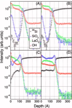
films, ToF SIMS depth profiles were acquired on ⬃10 nm thick La2O3film 共i.e., sample S5兲 in the as-grown state and
after annealing. In Fig.4, the ToF SIMS profiles of as-grown sample共A兲 are compared with those acquired after RTA per-formed in vacuum at 400 共B兲, 600 共C兲 and 800 °C 共D兲. In good agreement with the HRTEM findings, the presence of an IL in the as-grown sample is revealed by monitoring the SiO3 peak, as displayed in Fig. 4共a兲, thus suggesting the
presence of a SiOx-like component which coexists with the
La-based profile 共i.e., LaO2兲 in the region at the film/
substrate interface. In addition, in the as-grown film, the SiO3and 30Si signals detected at the surface reveal a mod-erate Si diffusion occurring through the La2O3 film during the ALD growth. Finally, the depth profile of the OH signal in Fig.4共a兲confirms the results of the GIXRD data analysis further attesting the marked hygroscopicity of the as-grown La2O3 films. The analysis of the ToF SIMS depth profiles after the 400 ° C thermal treatment 关Fig. 4共b兲兴 reveals that the chemical composition of the film has not been signifi-cantly affected by such a relatively low temperature anneal-ing process. Indeed, the IL seems stable in terms of thickness and composition and the Si distribution throughout the layer does not appear modified. Interestingly, despite the annealing process is performed in vacuum, the OH profile is slightly altered, in good agreement with the GIXRD results. No sig-nificant modifications in the structure of the layer are re-vealed, thus confirming that a full La共OH兲3conversion
can-not be accomplished at an annealing temperature of 400 ° C. In Fig. 4共c兲, the depth profiles of the sample annealed at 600 ° C are reported. A clear reduction in the intensity of the OH signal is observed, in accordance with the structural analysis, hence supporting the hypothesis of the La共OH兲3
conversion into h-La2O3upon annealing at 600 ° C. The30Si
signal indicates that Si atoms diffusion, from the substrate
FIG. 2. 共Color online兲 Electron density profiles extracted from the simula-tion of XRR data for as-grown共dotted line兲 and annealed in vacuum at 600 ° C共continuous line兲 ⬃20 nm thick films deposited on Si共100兲 共sample S4兲.
FIG. 3. HRTEM cross sections of ⬃20 nm thick 共a兲 as-grown and 共b兲 annealed La2O3/Si stacks 共sample S4兲. Dotted white lines are a guide for the eyes to visualize the borderline between the amorphous and the crystalline parts of the film.
FIG. 4.共Color online兲 ToF SIMS depth profiles acquired on ⬃10 nm thick films deposited on Si共100兲 共sample S5兲; as-grown 共a兲 and annealed in vacuum at 400共b兲, 600 共c兲, and 800 °C 共d兲.
through the film, occurred during the thermal treatment. Ac-cording to all the above results, the stack order atop the Si substrate after RTA at 600 ° C can be roughly approximated by a trilayer structure composed by an amorphous IL共most likely LaSiO species兲, a crystalline layer characterized by a decreasing Si content and a very thin La共OH兲3surface layer.
The presence of such a thin La共OH兲3capping layer might be
explained either by a not complete removal of the hydroxide component during the thermal treatment or by a rehydroxy-lation occurred during exposure to air before the ToF SIMS measurements. When the annealing temperature is increased up to 800 ° C 关Fig. 4共d兲兴, the thin La共OH兲3 layer vanishes
and no further reduction in the OH signal intensity is de-tected. Moreover, the 30Si signal in Fig.4共d兲 assumes a flat profile along the whole stack thickness indicating that, with a high temperature thermal treatment, Si diffusion from the substrate throughout the entire stack thickness is promoted. However, this finding does not imply that the whole layer should be considered fully converted into LaSiO species. In-deed, the layer is most likely composed by a mixture of hexagonal La2O3 and LaSiO phases or could present Si at-oms at the grain borders of the crystalline hexagonal La2O3. It is important to note that from GIXRD measurements we do not detect the formation of crystalline LaSiO phases.
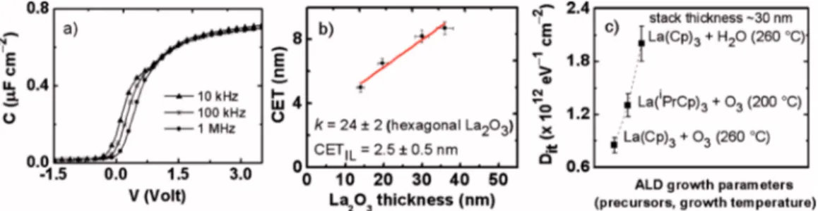
B. Electrical properties
Figure 5共a兲 illustrates multifrequency C-V curves ob-tained for the sample S4 annealed in vacuum at 600 ° C. Accumulation capacitance exhibits minor frequency disper-sion within the 10–1000 kHz range. From the slope of a linear fit to a CET versus La2O3thickness plot shown in Fig.
5共b兲, the k value for the annealed La2O3films is calculated to be 24⫾2. According to the structural analysis, La2O3
thick-ness is calculated by using the stack thickthick-ness corrected with a 5 nm thick IL; such an IL was considered independent on the total film thickness. The presence of the ultrathin La共OH兲3 capping layer, as detected by ToF SIMS analysis,
was neglected. Annealed samples taken under consideration in the CET plot of Fig. 5共b兲 are S1, S2, S3, and S4. In agreement with our GIXRD data, the extracted k value con-clusively confirms that RTA at 600 ° C in vacuum induces film crystallization into the h-La2O3 phase. It is noted that
the lowest boundary associated with the k value derived here for the h-phase falls outside the typical range cited in the literature,6,7 thus, suggesting a possible coexistence of the crystalline part with an amorphous silica-based phase which
is affecting the dielectric response of the whole stack. The fit in Fig.5共b兲intercepts with the y-axis at a point correspond-ing to an IL with a CET of about 2.5⫾0.5 nm which, in turn, yields, assuming the k value for the IL to be⬃11 共Ref.
15兲 an IL physical thickness of around 6–8 nm. This finding
is in line with both HRTEM and ToF SIMS results, acquired on the sample annealed at 600 ° C, where a significant Si diffusion, associated with the formation of LaSiO species, has been evidenced through about half共⬃5 nm兲 of the ap-proximately 10 nm thick stack. An actual high k, which gradually points to the expected value of 27, could be prob-ably obtained via increasing the total thickness of the elec-trical samples. The elecelec-trical analysis has been limited to the samples in which the structure, after annealing, can be mainly considered h-La2O3 and in which the interfacial re-gion constitutes only a reasonably small part of the whole stack. On the contrary, in very thin films 共⬍10 nm; e.g., samples S5 and S6兲 the k value would probably point to a value typical for LaSiO共⬃11兲 rather than to the one associ-ated to the h-phase. However, it is worth considering that the electrical analysis performed on the samples grown using the O3-based ALD recipe discussed in this work reveals the pos-sibility to obtain h-La2O3 for a reduced stack thickness than the ones we have previously reported.6,7,15 This finding is associated to the obtainment of a less extended LaSiO region at the interface by means of the use of O3and probably also
of a lower growth temperature. The restrainment of the in-terfacial LaSiO region permits the crystallization of a more extended part of the film into h-La2O3and consequently the
scaling down of the total EOT. Figure 5共c兲displays the av-erage Dit, as derived from loss peak of the GV curve at 100
kHz共Hill–Coleman method58兲, for three La2O3-based stacks
which are of similar thickness 共⬃30 nm兲 prepared on Si共100兲 using different combinations of ALD precursors, namely, 共i兲 La共Cp兲3+ H2O,6 共ii兲 La共Cp兲3+ O3,15 and 共iii兲
La共iPrCp兲
3+ O3 共this work兲. Although the ALD precursor
scheme tested in this study is very effective in stabilizing the
h-La2O3phase at a smaller sample thickness compared to the
cases in Ref.15, it generates, as manifested through the C-V stretch out and frequency-dependent hump in Fig. 5共a兲, a sizable Ditwhich must be further reduced in order to fulfill
advanced gate stack technology requirements.
As far as the Ditis concerned, in this work we confirm
the trend proposed in Ref.15that O3turns out to be a better
oxygen precursor choice than H2O. Nevertheless, because of
the different growth temperatures employed in the various ALD processes, it is not possible to make a direct
compari-FIG. 5. 共Color online兲 共a兲 C-V curves for Si-based MOS capacitors including ⬃20 nm of La2O3annealed at 600 ° C in vacuum共sample S4兲. 共b兲 CET plot
vs La2O3physical thickness共c兲 Comparison between Ditvalues obtained on La2O3/Si stacks prepared with different ALD recipes.
son between the two lowest Ditvalues obtained using the two
O3-based ALD recipes. We should also bear in mind that an
increase in growth temperature plays a key role in determin-ing the oxide/semiconductor interface electrical quality and therefore the Dit.
IV. LA2O3FILMS ON GE„100…
A. Structural and chemical properties
We analyze by means of GIXRD the crystallographic ordering of La2O3 as-grown and annealed films, deposited
using the O3-based ALD recipe on native oxide free Ge共100兲.
The measurements were performed immediately after the growth or the annealing treatment in order to minimize the effect of air exposure. The powder patterns of hexagonal La共OH兲3 共Ref.56兲 and La2O3共Ref. 57兲 are added for
com-parison with the spectra acquired for the sample G1. No clear evidence of crystallographic ordering is found in the as-grown film 共Fig.6兲, the latter result is attributed to the
ab-sence of long range order due to the mixture of La-based hydroxides. Differently, a single broad peak in the two theta ⬃29° region is visible after RTA at 400 °C. The two theta position of this peak corresponds to the increase in the long range order. Annealing at 600 ° C promotes a more pro-nounced crystallization of the La2O3in its h-phase. The lat-tice parameters extracted from the Rietveld refinement of the GIXRD data are a = 3.96⫾0.01 Å and c=6.26⫾0.01 Å, slightly higher than those obtained for the films deposited using the same ALD recipe on Si共100兲 and annealed at the same temperature.
The profiles, extracted by simulating the XRR curves of as-grown and 400 ° C annealed samples共Fig.7兲, support
the fact that the as-grown layers are mainly composed by La hydroxides formed by the incorporation of OH groups upon air exposure. Profiles are superimposed at the Ge共100兲 inter-face. Upon RTA performed at 400 ° C in vacuum, the density of the La-based layer is found to increase up to a value which approaches the one reported for h-La2O3. For the as-grown
state 共Fig. 7, dotted line兲, XRR reveals a decrease in the
close to the interface with Ge共100兲 that might be related to the formation of a less dense interfacial region. Differently, the value of the extracted after annealing共Fig.7, continu-ous line兲 appears uniform along the whole film thickness.
This finding might be tentatively explained with the hypoth-esis that theof the LaGeO species, that is likely forming at the La2O3/Ge interface upon annealing, is similar to theof
the h-La2O3 polymorph. Indeed, the values reported for
crystallized lanthanum germanates vary in the 1.38– 1.45 e−/Å3 range. Therefore, differently than for the
films deposited on H-terminated Si共100兲, from the profiles it is not possible to clearly define the extension of the inter-facial region.
Additional structural information with nanometric-scale resolution is provided for both as-grown and annealed La2O3 films by HRTEM analysis. Figure 8 shows HRTEM images of La2O3film共i.e., sample G3兲 deposited on Ge共100兲. In the
as-grown film 关Fig. 8共a兲兴 there is no evidence of a “struc-tural” amorphous IL, despite an O3-based ALD process
might be expected to promote an oxidation of the Ge共100兲 cleaned surface during the deposition.59Moreover, after RTA from the HRTEM cross section shown in Fig. 8共b兲 it is not possible to identify an amorphous structural IL atop the Ge共100兲. Nanocrystals can be identified within the film in both cases. However, the presence of the nanocrystals is more evident after annealing, in agreement with an increase in the crystalline order suggested by GIXRD analysis. The HRTEM findings hence support the conclusions of the struc-tural characterization; there is no evidence of the formation of an IL during O3-based growth and the film/substrate
inter-face looks sharp even after RTA.
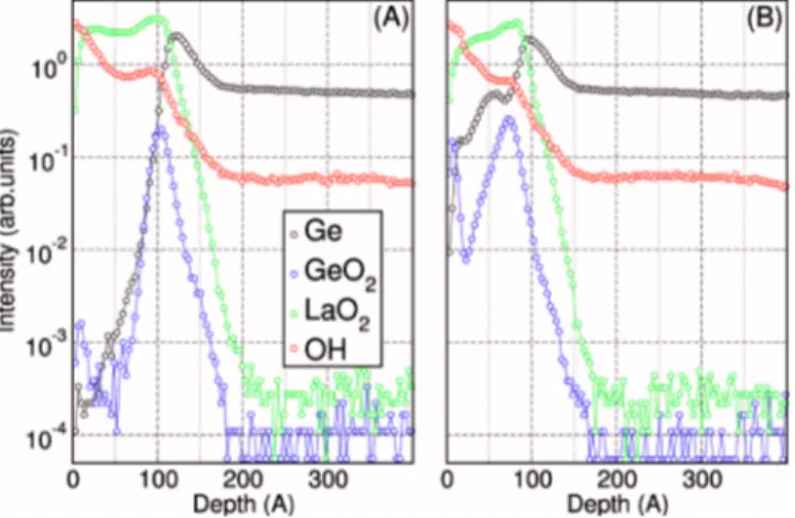
In order to assess the chemical composition within the film and at the interface with Ge共100兲, ToF SIMS depth pro-files were acquired on sample G2 in the as-grown state and
FIG. 6. 共Color online兲 GIXRD spectra acquired for as-grown and annealed in vacuum共400 and 600 °C兲 ⬃20 nm thick films 共sample G1兲 deposited on Ge共100兲. Hexagonal La共OH兲3and hexagonal La2O3patterns are added for
comparison.
FIG. 7. 共Color online兲 Electron density profiles extracted from the simula-tion of XRR data for as-grown共dotted line兲 and annealed in vacuum at 400 ° C共continuous line兲 ⬃20 nm thick film deposited on Ge共100兲 共sample G1兲.
FIG. 8. HRTEM cross sections of ⬃10 nm thick 共a兲 as-grown and 共b兲 annealed at 400 ° C in vacuum La2O3/Ge stacks 共sample G3兲.
after annealing at 400 ° C. In Fig. 9共a兲, the intense GeO2
signal at the La2O3/Ge interface indicates the presence of a
Ge-rich interfacial region already in the as-grown sample. Given the aforementioned XRR and HRTEM results, such a GeO2 signal can be attributed to the presence of a dense lanthanum germanate region of undefined thickness exten-sion. Therefore, ToF SIMS indicates the presence of a so-called “chemical” IL as already observed for La-doped ZrO2
films deposited on Ge共100兲.51
No intense Ge related signals are detected at the surface of the La2O3 film, suggesting a limited Ge diffusion during ALD growth. As expected, in the as-grown state the shape of the OH profile unveils the pres-ence of a relevant hydroxide component in the film. After annealing at 400 ° C 关Fig. 9共b兲兴, the OH profile is only slightly modified. As already demonstrated for the La2O3/Si stack, such low thermal budget is not sufficient to promote the complete removal of the La共OH兲3 component. The Ge and GeO2 signals appear more extended into the layer
indi-cating that Ge diffusion has occurred during RTA. The graded Ge profile detected inside the La2O3layer results in a not uniform Ge distribution along the thickness of the film. Therefore, atop a chemical IL composed mainly by LaGeO, the h-La2O3 nanocrystals coexist with a graded Ge profile
through the film; Ge atoms could be located at the grain borders. We believe that the use of a higher postdeposition annealing temperature or of a longer annealing time, would probably promote a further diffusion of Ge through the whole film thickness.
B. Electrical properties
C-V characteristics acquired for sample G1 are shown in
Fig. 10共a兲. The hysteresis corresponds to trapped positive charges, probably related to the incomplete OH desorption or to the not optimal saturation of the defects at or close to the interface with Ge. From the CET versus La2O3thickness plot
关Fig.10共b兲兴, a k value of 22⫾1 is calculated for the set of
annealed films共i.e., samples G1, G2, and G3兲. This value is in line with the highest boundary reported in literature for the range of k values associated to h-La2O3 on Ge共100兲.
Al-though slightly smaller, the k value appears to be in fairly good agreement with the one calculated for the same films deposited on Si共100兲. The difference could be associated to a more efficient conversion of the hydroxide layer into
h-La2O3 phase occurring in the La2O3/Si stacks annealed at
600 ° C. Moreover, in these Ge-based stacks the identifica-tion of a clear IL is extremely complex. The k value was extracted reasonably assuming a 2 nm thick IL and thus cal-culating the resulting La2O3thickness. The extraction of the
dielectric constant is not affected by this assumption. On the contrary, the discussion of the CET intercepts 共⬃2.4⫾0.5 nm assuming the IL thickness at 2 nm兲 with the
y-axis must be addressed with particular care because of the
uncertainties on the thickness and k of the IL that are likely to be modified upon RTA. We are prone to believe, also referring to the literature reports about La2O3/Ge stacks, that also in our system a lanthanum germanate compound 共k ⬃5–6兲 should be present at the interface. Therefore, the actual thickness of the “chemical” IL could be larger than 2 nm. Nevertheless, in order to address this specific issue a more detailed chemical investigation of the interface compo-sition is needed60as extensively discussed in Ref.51. The Dit should be extracted at high frequency, and thus at more posi-tive voltages, in order to be in the depletion regime. How-ever, values extracted at lower frequency could yield to an overestimation of the Ditsince in the weak inversion regime
also the minority carriers contribute to the conductance mechanisms. For this reason, Ditvalues were evaluated with
the Hill–Coleman method58 at 500 kHz. The Ditis found to
be ⬃3.5⫻1012 eV−1cm−2, independently of the film thick-ness. Ditvalues obtained for the annealed samples considered
in this work are compared, in Fig.10共c兲, to data reported in literature for annealed La2O3/Ge stacks. It is worth noticing that, with the present work, we confirm the trend that the use of O3 共Ref. 54兲 associated to the presence of La at the
interface29,51turns out to be helpful in keeping the Ditvalue
FIG. 9.共Color online兲 ToF SIMS depth profiles acquired on ⬃15 nm thick 共sample G2兲 as-grown 共a兲 and annealed at 400 °C 共b兲 films deposited on Ge共100兲.
FIG. 10.共Color online兲 共a兲 C-V curves for Ge-based MOS capacitors including ⬃15 nm of La2O3annealed at 400 ° C in vacuum共sample G1兲. 共b兲 CET plot
vs La2O3physical thickness.共c兲 Comparison between Ditvalues obtained on La2O3/Ge stacks prepared with different growth techniques.
relatively low due to the formation of LaGeO species.26,28 Because of the different growth temperatures and postdepo-sition annealing treatments employed in the different papers, it is not possible to make a direct comparison between the Dit
values. However, it is worth considering that Song et al.21,23 reported that, with vacuum annealing, it is possible to obtain a larger stack capacitance although associated with higher Dit
values. This observation is in line with our discussion about the efficiency of the vacuum annealing treatment in promot-ing, with a better efficiency, the formation of the h-La2O3
phase. The lowest Ditvalue presented in Fig.10共c兲was
in-deed associated in Ref.24to the use of high deposition tem-perature 共360 °C兲 combined to the use of a postdeposition annealing in H2 ambient. This might explain the fact that
films discussed in this work, grown by ALD at 200 ° C, present a comparatively higher Ditvalue as also revealed in
the case of samples grown on Si共100兲.
V. DISCUSSION: SI- AND GE-BASED STACKS
The formation of h-La2O3phase upon RTA in vacuum of La2O3 films grown by ALD has been investigated in two different oxide/semiconductor stacks. From our study and from the comparison with literature results, it turns out that the stabilization of such a high permittivity phase actually depends on three main factors which are discussed and sum-marized in the following Secs. V A–V C.
A. ALD precursors
The structure of the as-grown La2O3films is determined not only by the growth temperature, as expected, but also by the choice of the ALD precursors 共i.e., La and O source兲. Indeed, in general as-grown La2O3 films may consist of a mixture in which an amorphous hydroxide part, formed dur-ing the H2O-based ALD process and/or upon exposure to air, coexists with a small amount of crystalline La共OH兲3 and/or
c-La2O3. The presence of the latter phase, which is charac-terized by a lower k value ⬃17 and therefore undesired, depends on the ALD recipe employed and was reported ei-ther for H2O- 共Refs. 7 and 41兲 or for O3-based growths.10
Therefore, how the different crystalline structures are gener-ated should be discussed also referring to the key role played by the La source in determining either the reactivity of the ALD process or the C and H impurities content in the film.61 The presence of La共OH兲3 and/or c-La2O3 in the as-grown
film affects and conditions the development of the hexagonal La2O3 polymorph during the postdeposition annealing. The
use of La共iPrCp兲
3, at a growth temperature of 200 ° C and in
combination with O3, leads to the obtainment of almost fully
amorphous layers. As-grown films convert into La共OH兲3
upon air exposure while there is no evidence of the presence of the c-La2O3 phase. Subjected to RTA in vacuum these
films can be transformed into h-La2O3as it has been
demon-strated by GIXRD analysis and by the electrical character-ization.
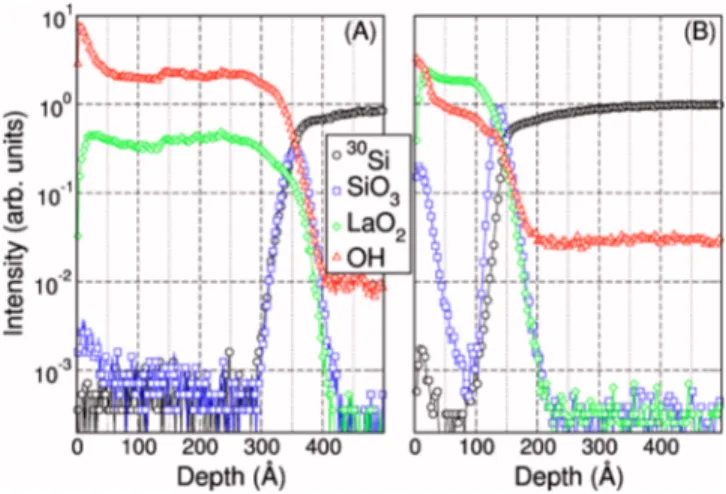
On the other hand, for the deposition of an extremely hygroscopic compound, the selection of the oxygen source appears to be even more critical. Figure 11共a兲 displays the ToF SIMS depth profiles acquired for the sample S7 _ H2O
共as-grown, ⬃38 nm兲, deposited using the H2O-based ALD
recipe while in Fig.11共b兲the signals related to the sample S5 共as-grown, ⬃10 nm兲 deposited using O3are plotted. OH and
LaO2 profiles are markedly different in the two cases. The
film grown using H2O as oxygen source presents a relatively
low LaO2 signal accompanied by a very intense OH emis-sion. Moreover the sample is characterized by an almost uni-form OH distribution along the whole film thickness thus suggesting a complete hydroxylation occurred directly dur-ing ALD and related to the continue exposure to a H2O rich ambient. Differently, the film deposited using O3presents a high LaO2 signal and low OH secondary ion emission. The different intensity of the LaO2 signal in the two samples is
undoubtedly related to a variation in the film composition. O3 provides a clear improvement in reducing the undesired
incorporation of OH that may occur during the growth thus disturbing the pure ALD behavior and promoting chemical vapor deposition side-reactions.43Finally, the selection of the oxygen source strongly affects diffusion mechanism at the oxide/semiconductor interface during the film growth. Dif-ferent 30Si and SiO3 signals are detected in the two cases
providing indication of a Si out-diffusion and segregation at the oxide surface in the film grown using O3as oxygen
pre-cursor. Considering that the films were grown at the same temperature, we can explain this experimental evidence as a consequence of the obtainment of two clearly distinct films from the chemical viewpoint.
B. Postdeposition thermal treatment
The results presented in this work confirm that the post-deposition thermal treatment must be properly selected while addressing the final properties of the annealed oxide. Indeed, the use of vacuum annealing technology共⬃1 mbar兲 plays a crucial role in reducing the OH content and removing the undesired hydroxide component from the La2O3 layers.6,8
However, due to a fairly insufficient removal of the OH groups, only a limited increase in the long range order can be promoted in films annealed at 400 ° C.7,62Actually, the crys-tallization into the h-polymorph is accomplished when the thermal treatment is performed in vacuum and concurrently
FIG. 11. 共Color online兲 ToF SIMS chemical depth profiles acquired on 共a兲 ⬃38 nm thick as-grown film deposited using the H2O-based ALD recipe
共sample S7_H2O兲 and 共b兲 ⬃10 nm thick as-grown film deposited using
the annealing temperature is 600 ° C, thus considerably re-moving the hydroxide and hence promoting the phase trans-formation. It is noted that a relevant chemical reaction at the La2O3/substrate interface is induced by such a postdeposition
annealing. Nevertheless, in order to preserve the high k value obtained upon vacuum annealing, an ultimate compatible de-vice process flow should be implemented and refined in or-der to completely solve the serious hygroscopicity issue re-lated to the use of h-La2O3 films in an actual industrial
process.
C. Si and Ge diffusion: Formation of LaSiO and LaGeO species
As far as the stabilization of h-La2O3 is concerned, the nature and the extension of the interface between the film and the substrate play a crucial role. Indeed, both on Si共100兲 and on Ge共100兲 a significant reactivity between the La, Si, and Ge species has been revealed and the formation of a structural and/or a chemical IL has been demonstrated. In this respect, we have systematically investigated the struc-tural and chemical evolution of the La2O3/substrate as-grown
and annealed interfaces in order to unravel their repercus-sions on the h-La2O3stabilization. On H-terminated Si共100兲
the use of a powerful oxidizing agent such as O3 promotes,
during the ALD growth, the formation of an amorphous SiOx-like IL. In addition to that, Si atoms are detected by
ToF SIMS also few nanometers beyond the IL, within the as-grown La2O3 layer. This means that, before the RTA a
portion of the stack presents a silica/silicate-like composi-tion. Upon annealing Si diffusion is further promoted through the film giving rise to the formation of a more ex-tended interfacial region. To explain the formation of this complex interface structure we can refer to the fact that silica readily reacts with La2O3 forming LaSiO species.15
Regard-less of the employed growth technique, LaSiO formation was indeed already reported either in as-deposited or in annealed La-based stacks.63,64 Since the formation of such a LaSiO region can be mainly attributed to thermodynamical factors, it can be considered independent of the total film thickness. On the contrary, the total film thickness plays a fundamental role in establishing the electrical properties of the annealed layers. In light of the observations made by XRD and ToF SIMS on films of different thickness, we can infer that the amount of La共OH兲3 that can be actually crystallized in the
h-La2O3phase directly depends on the amount of Si which is
present in the layer. Indeed, in thin films 共⬍10 nm兲 where the Si diffusion process involves almost the full stack thick-ness, it is not possible to achieve a complete crystallization into the h-phase thereby promoting LaSiO formation only. A different situation is revealed in La2O3/Ge stacks. HRTEM
cross section does not reveal any amorphous IL; however, ToF SIMS profiles acquired on the as-grown sample suggest the presence of a chemical interfacial region in which La, Ge and O elements coexist. During ALD, the formation of La– O–Ge bondings occurs, as it has already been demonstrated in several works where La-based oxides were put directly in contact with Ge共100兲.26,28,51
Similarly to what it has been inferred for LaSiO, the formation of LaGeO is a spontaneous
reaction and does not depend on the total film thickness. The Ge atoms diffusion from the substrate is likewise promoted by the thermal treatment performed at 400 ° C and conse-quently the chemical IL extension is increased. Given the aforementioned considerations, the issue of formation of the
h-La2O3crystalline phase can be more accurately discussed.
We must bear in mind that LaSiO and LaGeO species cannot be reconverted into La2O3 by a thermal treatment but that
remain stable after annealing. Therefore, only the portion of the as-grown La2O3film which does not present a significant
amount of Si or Ge atoms inside can be crystallized into the
h-phase. Indeed, the presence of the latter elements inside the
film does not allow the conversion into h-La2O3.
In summary, the formation of a fairly extended LaSiO and LaGeO region at the oxide/semiconductor interface and the concomitant Si and Ge diffusion are critical in determin-ing the possibility of generatdetermin-ing a pure full h-La2O3layer. In
thin films, LaSiO共LaGeO兲 formation and Si共Ge兲 diffusion involve a considerable part of the oxide stack. Therefore, only a very limited portion of the layer can actually be con-verted into h-La2O3. The reactivity at the interface and the atoms diffusion promoted by the thermal treatment prevent the possibility of an aggressive scaling down of the EOT thus jeopardizing the electrical performances of the whole layer. The coexistence of a LaSiO共LaGeO兲 interfacial region with the h-La2O3 phase is therefore unavoidable and has to be
carefully taken into account. This leads to the definition of a so-called “critical thickness” being the minimum utilizable physical thickness of the films in order to obtain the desired dielectric response associated to the presence of h-La2O3
phase. Such a “critical thickness,” for as-grown films depos-ited using the ALD recipe discussed in this work, was found to be of the order of 20 nm on H-terminated Si共100兲 and 10 nm on native oxide free Ge共100兲. As a consequence of this, samples S5, S6, and G4 were not employed for the electrical characterization. The possibility to scale down the La2O3
film thickness more on Ge共100兲 rather than on Si共100兲 can be explained considering that, because of the RTA performed at lower temperature 共i.e., 400 °C兲, the Ge atoms diffusion in annealed samples is less pronounced. However, it must be noted that the use of such an annealing temperature presents also the drawback of a fairly incomplete OH removal.
VI. CONCLUSIONS
We have deposited with ALD, using La共iPrCp兲
3and O3
species, smooth, thin, and uniform La2O3 films on both
H-terminated Si共100兲 and on native oxide free Ge共100兲 sub-strates at the growth temperature of 200 ° C. The oxide is found amorphous in the as-deposited state. It readily reacts with moisture upon air exposure thus forming lanthanum hy-droxide. However, films can be successfully converted into hexagonal h-La2O3upon RTA performed in vacuum
environ-ment. Such an O3-based ALD process allows to obtain films
in which there is no evidence of the low-k cubic La2O3
phase, neither before, nor after postdeposition annealing. The main aims of this work were to validate the use of O3 as
suitable oxygen source to be employed in ALD of La2O3and
to demonstrate the production of hexagonal h-La2O3on two
different semiconductor substrates. For films grown on Si共100兲, after RTA performed at 600 °C in vacuum, a dielec-tric constant k of 24⫾2 is obtained. Despite the amorphous SiOx-like IL and the thermally promoted Si diffusion, which
give rise to the formation of a LaSiO interfacial region, the employment of the O3-based ALD process results in the
pos-sibility to obtain h-La2O3in a 19.7 nm thick annealed film.
This finding is here associated with the formation of a rea-sonably limited SiOx- and LaSiO-like interfacial region. The
films grown with the same ALD recipe on native oxide free Ge共100兲 present, after RTA in vacuum at 400 °C, a k value of 22⫾1. It is evidenced the presence of a LaGeO region at the interface between the semiconductor and the oxide. Al-though such interface reactivity limits the generation of hex-agonal h-La2O3; a fairly high k value is demonstrated for a
6.8 nm thick annealed film. Moreover, the use of O3
accom-panied by the formation of LaGeO at the interface provides the possibility to obtain acceptably low Ditvalues.
In conclusion, an O3-based ALD recipe has been dis-cussed as a viable way to obtain hexagonal La2O3films both on Si and on Ge. We have addressed the stabilization of the high-k hexagonal phase focusing the attention on the impact of the oxide/semiconductor interface characteristics on the overall electrical performances of the stack. These studies lead to the identification of a “critical thickness” that, al-though reduced, still limits an aggressive scaling down of the EOT both on Si and on Ge. However, the employment of the hexagonal La2O3 obtained using this ALD recipe might
re-sult in a promising solution for different stacks. The deposi-tion of the high-k phase on alternative substrates might allow a further reduction in the total film thickness and conse-quently of the final EOT.
ACKNOWLEDGMENTS
This work was supported by the European FP6-Program “REALISE”共Grant No. IST-NMP 016172兲.
1D. G. Schlom, S. Guha, and S. Datta, MRS Bull. 33, 1017共2008兲. 2B. H. Lee, S. C. Song, R. Choi, and P. Kirsch, IEEE Trans. Electron
Devices55, 8共2008兲.
3M. Bohr, R. Chau, T. Ghani, and K. Mistry,IEEE Spectrum44, 29共2007兲. 4Rare Earth Oxide Thin Films: Growth, Characterization, and
Applica-tions, Topics in Applied Physics, edited by M. Fanciulli and G. Scarel
共Springer, Berlin, 2007兲, Vol. 106, pp. 1–14.
5J. Robertson,J. Appl. Phys.104, 124111共2008兲.
6G. Scarel, A. Debernardi, D. Tsoutsou, S. Spiga, S. C. Capelli, L.
Lama-gna, S. N. Volkos, M. Alia, and M. Fanciulli,Appl. Phys. Lett.91, 102901 共2007兲.
7D. Tsoutsou, G. Scarel, A. Debernardi, S. C. Capelli, S. N. Volkos, L.
Lamagna, S. Schamm, P. E. Coulon, and M. Fanciulli,Microelectron. Eng. 85, 2411共2008兲.
8Y. Zhao, K. Kita, K. Kyuno, and A. Toriumi,Appl. Phys. Lett.94, 042901
共2009兲.
9S. Jeon and H. Hwang,J. Appl. Phys.93, 6393共2003兲.
10M. Nieminen, M. Putkonen, and L. Niinistö,Appl. Surf. Sci.174, 155
共2001兲.
11Y. Zhao, M. Toyama, K. Kita, K. Kyuno, and A. Toriumi,Appl. Phys. Lett.88, 072904共2006兲.
12X. Li, D. Tsoutsou, G. Scarel, C. Wiemer, S. C. Capelli, S. N. Volkos, L.
Lamagna, and M. Fanciulli,J. Vac. Sci. Technol. A27, L1共2009兲. 13Y. Zhao, K. Kita, K. Kyuno, and A. Toriumi,Jpn. J. Appl. Phys., Part 146,
4189共2007兲.
14H. Ono and T. Katsumata,Appl. Phys. Lett.78, 1832共2001兲.
15S. Schamm, P. E. Coulon, S. Miao, S. N. Volkos, L. H. Lu, L. Lamagna, C.
Wiemer, D. Tsoutsou, G. Scarel, and M. Fanciulli,J. Electrochem. Soc. 156, H1共2009兲.
16G. Lippert, J. Dąbrowski, V. Melnik, R. Sorge, Ch. Wenger, P. Zaumseil,
and H. J. Müssig,Appl. Phys. Lett.86, 042902共2005兲.
17D. Rébiscoul, S. Favier, J. P. Barnes, J. W. Maes, and F. Martin, Micro-electron. Eng.87, 278共2010兲.
18B. H. Lee, J. Oh, H. H. Tseng, R. Jammy, and H. Huff,Mater. Today9, 32
共2006兲.
19Y. Kamata,Mater. Today11, 30共2008兲.
20J. Song, K. Kakushima, P. Ahmet, K. Tsutsui, N. Sugii, T. Hattori, and H.
Iwai,Jpn. J. Appl. Phys., Part 246, L376共2007兲.
21J. Song, K. Kakushima, P. Ahmet, K. Tsutsui, N. Sugii, T. Hattori, and H.
Iwai,Microelectron. Eng.84, 2336共2007兲.
22K. Kita, T. Takahashi, H. Nomura, S. Suzuki, T. Nishimura, and A.
Tori-umi,Appl. Surf. Sci.254, 6100共2008兲.
23J. Song, K. Kakushima, P. Ahmet, K. Tsutsui, N. Sugii, T. Hattori, and H.
Iwai,Microelectron. Eng.86, 1638共2009兲.
24G. Mavrou, S. Galata, P. Tsipas, A. Sotiropoulos, Y. Panayiotatos, A.
Dimoulas, E. K. Evangelou, J. W. Seo, and Ch. Dieker,J. Appl. Phys.103, 014506共2008兲.
25M. Houssa, G. Pourtois, M. Caymax, M. Meuris, and M. M. Heyns,Appl. Phys. Lett.92, 242101共2008兲.
26A. Dimoulas, D. Tsoutsou, Y. Panayiotatos, A. Sotiropoulos, G. Mavrou,
S. F. Galata, and E. Golias,Appl. Phys. Lett.96, 012902共2010兲. 27V. V. Afanas’ev, A. Stesmans, G. Mavrou, and A. Dimoulas,Appl. Phys.
Lett.93, 102115共2008兲.
28G. Mavrou, P. Tsipas, A. Sotiropoulos, S. F. Galata, Y. Panayiotatos, A.
Dimoulas, C. Marchiori, and J. Fompeyrine,Appl. Phys. Lett.93, 212904 共2008兲.
29S. F. Galata, G. Mavrou, P. Tsipas, A. Sotiropoulos, Y. Panayiotatos, and
A. Dimoulas,J. Vac. Sci. Technol. B27, 246共2009兲.
30S. Abermann, O. Bethge, C. Henkel, and E. Bertagnolli,Appl. Phys. Lett. 94, 262904共2009兲.
31C. Andersson, C. Rossel, M. Sousa, D. J. Webb, D. Caimi, H. Siegwart, Y.
Panayiotatos, A. Dimoulas, and J. Fompeyrine,Microelectron. Eng.86, 1635共2009兲.
32S. Guha, E. Cartier, M. A. Gribelyuk, N. A. Bojarczuk, and M. C. Copel, Appl. Phys. Lett.77, 2710共2000兲.
33S. Stemmer, J. P. Maria, and A. I. Kingon, Appl. Phys. Lett.79, 102
共2001兲.
34T. M. Pan, C. L. Chen, W. W. Ye, and W. J. Lai,Electrochem. Solid-State Lett.10, H101共2007兲.
35S. W. Kang and S. W. Rhee,J. Electrochem. Soc.149, C345共2002兲. 36C. Bedoya, G. G. Condorelli, S. T. Finocchiaro, A. Di Mauro, D. Atanasio,
I. L. Fragalà, L. Cattaneo, and S. Carella,Chem. Vap. Deposition12, 46 共2006兲.
37H. Nohira, T. Shiraishi, K. Takahashi, T. Hattori, I. Kashiwagi, C.
Ohs-hima, S. Ohmi, H. Iwai, S. Joumori, K. Nakajima, M. Suzuki, and K. Kimura,Appl. Surf. Sci.234, 493共2004兲.
38Y. H. Lin, C. H. Chien, T. Y. Yang, and T. F. Lei,J. Electrochem. Soc.154,
H619共2007兲.
39H. Kim, H. B. R. Lee, and W. J. Maeng,Thin Solid Films517, 2563
共2009兲.
40B. Y. Kim, M. G. Ko, E. J. Lee, M. S. Hong, Y. J. Jeon, and J. W. Park, J.
Korean Phys. Soc. 49, 1303共2006兲.
41W. He, S. Schuetz, R. Solanki, J. Belot, and J. McAndrew,Electrochem. Solid-State Lett.7, G131共2004兲.
42D. H. Triyoso, R. I. Hedge, J. M. Grant, J. K. Schaeffer, D. Roan, B. E.
White, Jr., and P. J. Tobin,J. Vac. Sci. Technol. B23, 288共2005兲. 43B. Lee, T. J. Park, A. Hande, M. J. Kim, R. M. Wallace, J. Kim, X. Liu, J.
H. Yi, H. Li, M. Rousseau, D. Shenai, and J. Suydam,Microelectron. Eng. 86, 1658共2009兲.
44J. M. Gaskell, A. C. Jones, P. R. Chalker, M. Werner, H. C. Aspinall, S.
Taylor, P. Taechakumput, and P. N. Heys,Chem. Vap. Deposition13, 684 共2007兲.
45D. Eom, S. Y. No, C. S. Hwang, and H. J. Kim,J. Electrochem. Soc.154,
G49共2007兲.
46S. D. Elliott, G. Scarel, C. Wiemer, M. Fanciulli, and G. Pavia,Chem. Mater.18, 3764共2006兲.
47D. H. Triyoso, R. Gregory, M. Park, K. Wang, and S. I. Lee,J. Electro-chem. Soc.155, H43共2008兲.
48J. Niinistö, K. Kukli, T. Sajavaara, M. Ritala, M. Leskelä, L. Oberbeck, J.
Sundqvist, and U. Schröder,Electrochem. Solid-State Lett.12, G1共2009兲. 49D. Tsoutsou, L. Lamagna, S. N. Volkos, A. Molle, S. Baldovino, S.
Schamm, P. E. Coulon, and M. Fanciulli,Appl. Phys. Lett.94, 053504 共2009兲.
50A. Delabie, A. Alian, F. Bellenger, M. Caymax, T. Conard, A. Franquet, S.
Sioncke, S. Van Elshocht, M. M. Heyns, and M. Meuris,J. Electrochem. Soc.156, G163共2009兲.
51L. Lamagna, C. Wiemer, S. Baldovino, A. Molle, M. Perego, S.
Schamm-Chardon, P. E. Coulon, and M. Fanciulli,Appl. Phys. Lett.95, 122902 共2009兲.
52J. Kwon, M. Dai, M. D. Halls, and Y. J. Chabal,Chem. Mater.20, 3248
共2008兲.
53J. B. Kim, D. R. Kwon, K. Chakrabarti, C. Lee, K. Y. Oh, and J. H. Lee, J. Appl. Phys.92, 6739共2002兲.
54D. Kuzum, T. Krishnamohan, A. J. Pethe, A. K. Okyay, Y. Oshima, Y.
Sun, J. P. McVittie, P. A. Pianetta, P. C. McIntyre, and K. C. Saraswat,
IEEE Electron Device Lett.29, 328共2008兲.
55C. Wiemer, S. Ferrari, M. Fanciulli, G. Pavia, and L. Lutterotti,Thin Solid Films450, 134共2004兲.
56Inorganic Crystal Structure Database, Fachinformationszentrum,
Karlsruhe, 2009, file no. 31584.
57Inorganic Crystal Structure Database, Fachinformationszentrum,
Karlsruhe, 2009, file no. 24693.
58W. A. Hill and C. C. Coleman,Solid-State Electron.23, 987共1980兲. 59S. Spiga, C. Wiemer, G. Tallarida, G. Scarel, S. Ferrari, G. Seguini, and
M. Fanciulli,Appl. Phys. Lett.87, 112904共2005兲.
60This work, that will be the subject of another publication, is on-going
using systematic coupling of HRTEM to electron energy-loss spectroscopy experiments giving access to elemental profiles across interfaces.
61S. D. Elliott,Surf. Coat. Technol.201, 9076共2007兲.
62N. K. Park, D. K. Kang, B. H. Kim, S. J. Jo, and J. S. Ha,Appl. Surf. Sci. 252, 8506共2006兲.
63J. S. Jur, D. J. Lichtenwalner, and A. I. Kingon,Appl. Phys. Lett.90,
102908共2007兲.
64M. Copel, E. Cartier, and F. M. Ross,Appl. Phys. Lett.78, 1607共2001兲.