Automation of Soft Lithographic Microcontact
Printing
by
Amar Maruti Kendale
Submitted to the Department of Mechanical Engineering
in partial fulfillment of the requirements for the degree of
Master of Science in Mechanical Engineering
at the
MASSACHUSETTS INSTITUTE OF TECHNOLOGY
February 2002
@
Massachusetts Institute of Technology 2002. All rights reserved.
A u th or ...
...
Department of Mechanical Engineering
January 18, 2002
C ertified by ...
David L. Trumper
Associate Professor of Mechanical Engineering
Thesis Supervisor
A ccep ted by ...
Ain A. Sonin
Chairman, Departmental Committee on Graduate Students
ASSACHUSETTS INSTITUTE OF TECHNOLOGY
3
Automation of Soft Lithographic Microcontact Printing
by
Amar Maruti Kendale
Submitted to the Department of Mechanical Engineering on January 18, 2002, in partial fulfillment of the
requirements for the degree of
Master of Science in Mechanical Engineering
Abstract
This thesis presents the design, fabrication, control, and test of an automated mi-crocontact printing tool. This four-axis tool has the capability to transfer two-dimensional micropatterns on a stamp master to a 100 mm diameter substrate. The patterning of specialized chemical inks enables the creation of high-resolution im-prints, which tailor a substrate surface with specific chemical or biological function-ality.
Using our microcontact printing tool, we are able to generate highly-ordered and regular patterns of micron-scaled cross and dot features. Preliminary testing and analysis of these micropatterns indicates that single-micron resolution is achievable.
We developed a novel hybrid force-position control scheme for the stamping pro-cess. Using a set of force-control actuators (voice coils) coupled with position sensing (capacitance gages), and a flexural guidance system, we are able to automatically level the stamp to the substrate and thereby achieve high-resolution uniform pressure control at the stamp-substrate interface.
As part of this thesis, we also developed a method of creating thin elastomeric stamps bearing microfeatures for patterning. The dimensional stability of the thin stamp is governed by a thick substrate. A fluid-based pressurized parting technique allows the separation of the rigidly-backed stamp and master without imparting large stresses to the delicate elastomeric part.
Thesis Supervisor: David L. Trumper
5
Acknowledgments
The two years I have spent at M.I.T. working on my Master's Degree have been extremely intellectually stimulating and rewarding. This project has been everything
I had hoped for and more, and it was only possible through the support of many
people.
First, I thank my family: my parents Maruti and Rajani, and my brother Samir. They have always given me their full support, encouragement, and unconditional love.
My father has been my inspiration as an engineer since I was a boy. My mother has
always made sure that I have had every opportunity to learn and grow. Samir is my favorite person to relax and unwind with.
Thanks go to my advisor, Professor David Trumper. Professor Trumper has been an ideal mentor through my thesis; I have learned more from him than I could learn from any course or textbook, and about far more than engineering. His vast knowledge of precision machine design and controls has also shown me how rewarding machine
building can be.
My labmates at the Precision Machine Control Laboratory have also been a great
asset to me, and it has been an honor to work alongside them. Mike Leibman taught me the basics of current amplifier design, and also gave me an introduction to State-flow. Marty Byl has been my comrade-in-arms as we strived to grasp the subtleties of Simulink and Stateflow. Rick Montesanti has been a wonderful resource for ma-chine design know-how, and I was fortunate to have his design critique. Andy Stein, Xiaodong Lu, Marty Vona, and Tsuyoshi Sato were always willing to lend a hand, and contributed many innovative design ideas.
Other members of the MIT staff helped me with my thesis as well. Dave Ro-driguera made purchasing a breeze. Mark Belanger and Gerry Wentworth at the Laboratory for Manufacturing Productivity taught me the essentials of machining, and helped me to appreciate the enormous skill and intuition that is required to make high-quality parts. Andrew Gallant at the Central Machine Shop was a great help in
6
contracting the fabrication of my more intricate components.
I owe a deep debt of gratitude to Dr. Carmichael Roberts, who placed an enormous amount of faith in me as my sponsor for this research. The team of scientists at Surface Logix that I have had the privilege to work with have been a tremendous inspiration. Dr. David Duffy guided me on my way in the early days as we specified the project scope. Dr. Enoch Kim has always been helpful, with his amazing depth and breadth of knowledge of chemistry and microfabrication. Dr. Olivier Schueller, another fabrication expert, helped me to make the photolithographic masters that are essential for microcontact printing, and to etch silver. Aaron Raphel patiently taught me the photolithographic process (many times), and how to evaporate metals. Towards the end of the project, Dr. Bernardo Aumond has been a great person with whom I could discuss controls and data analysis.
Last but not least, I thank my dear Prabha. She has been my best friend and constant supporter, and to her I offer my most heartfelt gratitude.
Contents
1 Introduction 19
1.1 Overview of Thesis Results . . . . 20
1.2 Overview of Microcontact Printing . . . . 25
1.3 Project Motivation . . . . 27
1.4 Project Approach . . . . 27
1.5 Design . . . . 28
1.6 Stamp Generation . . . . 38
1.7 Fabrication . . . . 41
1.8 Testing and Metrology . . . . 44
1.9 Thesis Contributions . . . . 47 1.10 Thesis Organization . . . . 47 2 Literature Review 49 2.1 Soft Lithography . . . . 49 2.2 Microcontact Printing . . . . 51 2.2.1 Inks . . . . 53 2.2.2 Stamps . . . . 55 2.2.3 Substrates . . . . 57 2.2.4 Contact Mechanics . . . . 58
2.2.5 Automation of Microcontact Printing . . . . 59
2.2.7 Other Relevant Fabrication Processes . . . .
2.3 M icrom olding . . . .
2.3.1 Generation of Masters . . . .
2.3.2 M olding Process . . . .
2.3.3 Conditioning and Preparation of Molded Structures
2.3.4 Metrology of Micromolded Structures . . . .
2.3.5 Other Relevant Micromolding Processes . . . .
3 Design of Our Microcontact Printing Tool 3.1 Design Overview ...
3.2 Functional Requirements . . . . 3.3 Design Parameters . . . .. 3.4 System Topology . . . . 3.4.1 Parallelization of stamp and substrate 3.4.2 Contact initiation and propagation . 3.4.3 Stamping force requirements . . . . . 3.4.4 Substrate fixturing and handling . .
3.4.5 Inking . . . .
3.5 Linear Stage Selection . . . . 3.5.1 Functional Requirements . . . .
3.5.2 Choice of Stage . . . .
3.5.3 Am plifier . . . .
3.6 Stamp Head Design . . . . 3.6.1 Functional Requirements . . . . 3.6.2 Design Parameters . . . . 3.6.3 Sensing . . . . 3.6.4 Actuation . . . . 3.6.5 Guidance . . . . planes
3.6.6 Mechanical Design of Stamp Head .
66 67 68 69 70 70 71 73 . . . . 74 . . . . 77 77 78 82 83 85 87 88 88 88 89 90 90 90 92 93 98 104 110
3.6.7 Pressure Chamber Design . . . . 112
3.7 Substrate Chuck Design . . . . 122
3.8 Machine Structure . . . . 124
3.8.1 Vibration Isolation Table . . . . 124
3.8.2 Surface Plate . . . . 125 3.8.3 Angle Brackets . . . . 126 4 Stamp Generation 127 4.1 Motivation . . . . 130 4.2 Approach . . . . 132 4.3 Fabrication of Masters . . . . 132 4.4 Molding . . . . 136 4.4.1 Mold Design . . . . 139 4.4.2 Molding Process . . . . 143
4.4.3 Parting Stamp from Master . . . . 144
4.5 Characterization of Stamp . . . . 148
5 Fabrication 151 5.1 Machining and Assembly of Molding Chamber . . . . 151
5.1.1 Rings . . . . 153
5.1.2 Angle Stand . . . . 153
5.2 Machining and Assembly of Stamp Head . . . . 156
5.2.1 Flexure fabrication . . . . 157
5.2.2 Stamp head assembly . . . . 159
5.3 Machining and Assembly of Printing Tool . . . . 162
5.3.1 Wafer chuck . . . . 162
5.3.2 Miscellaneous components . . . . 166
5.3.3 Plumbing . . . . 167
5.4 Sum m ary . . . . 6 Controls 6.1 Control D esign . . . . 6.1.1 System overview . . . . . 6.1.2 Systems characterization . . . . . 6.1.3 Stage Control . . . . 6.1.4 Stamp Head Control . . . . 6.1.5 System Control Strategy and Algorithm 6.2 Control Implementation . . . .
6.2.1 Modeling and Simulation Environment 6.2.2 DSP Board and User Interface . . . . . 6.3 Other Control Approaches . . . . 6.3.1 Closed-loop position control mode . . . 6.3.2 Impedance control . . . .
7 Testing and Metrology 7.1 Optical Microscopy of . . . . 1 7 8 . . . .. . 179 . . . . 1 7 9 . . . . 1 8 4 . . . . 1 9 7 . . . . 2 0 1 . . . . 2 0 1 . . . . 2 0 9 . . . . 2 1 0 . . . . 2 1 3 . . . . 2 1 4 215 Stamp Face . . . . 215 7.2 Testing Methodology . . . . 7.2.1 Initial testing . . . .
7.2.2 Semi-automatic active-pose, passive-force 7.3 Fully Automated Stamping . . . . 7.3.1 Substrate preparation . . . .
7.3.2 Inking . . . .
7.3.3 Stamping . . . .
7.3.4 Etching . . . .
7.3.5 R esults . . . . 7.3.6 Measurement of Feature Uniformity . . . 7.4 Summary . . . . . . . . 221 stamping 221 223 223 224 225 226 226 228 231 . . . . 237 172 175 176
8 Conclusions and Recommendations for Future Work 8.1 Conclusions . . . .
8.2 Recommendations for Future Research . . . .
8.2.1 Optimization of stamping pressure . . . .
8.2.2 Optimization of contact time . . . .
8.2.3 Active control of head stiffness . . . .
8.2.4 Automation of stamp generation . . . .
8.2.5 Alignment to substrate features or fiducials . . . .
8.2.6 Contact patch control . . . .
8.2.7 Automated stamp inking, drying, and cleaning . .
8.2.8 Automated substrate handling . . . .
8.2.9 Stamping on substrates with non-uniform flatness
8.2.10 Stamping on non-planar substrates . . . . 8.2.11 Aligned micro-embossing . . . . 8.3 Sum m ary . . . . A Calculations 239 . . . . 239 . . . . 240 . . . . 240 . . . . 241 . . . . 241 . . . . 242 . . . . 242 . . . . 243 . . . . 243 . . . . 244 . . . . 244 . . . . 245 . . . . 245 . . . . 245 247 B Part Drawings C List of Vendors 251 265
List of Figures
1-1 Photograph of microcontact printing machine . . . . 21
1-2 CAD model of printing tool . . . . 22
1-3 Photograph of stamp molding setup . . . . 23
1-4 Microcontact printed patterns, silver on silicon . . . . 24
1-5 Microcontact printing process. . . . . 26
1-6 M achine topology . . . . 30
1-7 Cross-sectional view of stamp head assembly . . . . 31
1-8 Cross-sectional view of stamp head assembly . . . . 32
1-9 Photograph of stamp head assembly, bottom view . . . . 33
1-10 CAD model of printing tool . . . . 34
1-11 Calibration procedure: al) Initial position; a2) Advance and record pose; a3) Retract, pose head, end calibration; bi) Ink stamp; b2) Con-tact substrate, transfer ink; b3) Retract . . . . 35
1-12 Control algorithm . . . . 37
1-13 CAD model of mold chamber assembly, cross-sectional view . . . . . 39
1-14 CAD model of machine . . . . 42
1-15 Photograph of stamp head assembly, bottom view . . . . 43
1-16 Photograph of fully assembled microcontact printing tool . . . . 44
1-17 Microcontact printed patterns, silver on silicon . . . . 46
2-2 Stamp backings: a) PDMS stamp with rigid backing; b) hybrid stamp with rigid backing; c) stiff stamp with flexible backing . . . .
3-1 3-2 3-3 3-4 3-5 3-6 3-7 3-8 3-9 3-10 3-11 3-12 3-13 3-14 3-15 3-16 3-17 3-18 3-h 3-2( 3-2 3-2 3-2 3-2 3-2 3-2 tional view 61 74 75 76 CAD model of microcontact printing tool . . . .
Stamp head assembly, cross-sectional view . . . .
CAD model of pressure chamber sub-assembly, cross-sec
M achine topology . . . . An alternate topology . . . . Radial contact propagation . . . . Linear contact propagation . . . . Rolling contact propagation . . . . Aerotech ATS 406 Linear Stage . . . .
CAD model of stamp head assembly, top view . . . . .
CAD model of stamp head assembly, bottom view . .
Thin-film stamp-mounted capacitance gages . . . . . Hertzian contact sensing scheme . . . . Stamp-side sensing scheme . . . . Stamp head assembly, cross-sectional view . . . . Stamp head assembly, cross-sectional view . . . . Current amplifier schematic . . . . Degrees of freedom . . . . Orthogonally oriented notch hinges . . . . Flexure variations . . . .
I Rolled diaphragm flexure, with section cut . . . . 2 CAD model of flexure . . . . 3 Cross-sectional view of stamp head assembly . . . . . I CAD model of pressure chamber assembly . . . . 5 CAD model of pressure chamber sub-assembly, cross-s 6 Initiation and propagation of a contact front . . . . .
ectional view 113 114 . . . . 79 . . . . 82 . . . . 84 . . . . 85 . . . . 86 . . . . 89 . . . . 91 . . . . 92 . . . . 93 . . . . 95 . . . . 96 . . . . 98 . . . . 99 . . . . 102 . . . . 104 . . . . 105 . . . . 105 . . . . 106 . . . . 108 . . . . 110 . . . . 112
3-27 Effects of thermal expansion: a) low CTE and high thermal
conduc-tivity; b) high CTE; c) low thermal conductivity. . . . .
3-28 Stamp mounting using a hemi-toroidal coupling . . . . 3-29 CAD model of chuck assembly . . . . 3-30 CAD model of microcontact printing tool . . . .
3-31 CAD model of angle brackets . . . .
4-1 4-2 4-3
CAD model of mold chamber assembly, cross-sectional view . . . . .
Photograph of stamp molding setup . . . . Crosses in PDMS stamp face (crosses are 500 pm by 500 pm, with
linewidths of 100 pm ) . . . . 116 121 123 125 126 128 129 130
Dots in PDMS stamp face (dots are 100 pm in diameter) . . Mask, master, stamp, and printed pattern . . . . Recessed crosses in SU-8 photoresist . . . . Recessed dots in SU-8 photoresist . . . . Molding proof-of-principle experiment . . . . Schematic detail of mold chamber (not to scale) . . . . CAD model of mold chamber assembly, cross-sectional view
. . . . . 130 . . . . . 133 . . . . . 136 . . . . . 136 . . . . . 138 .140 . . . . . 142 4-11 Mold chamber . . . . 4-12 Molding setup . . . . 4-13 Angled interface for stamp-master parting . . . . 4-14 M olding Setup . . . . 4-15 Crosses in PDMS stamp face (crosses are 500 pm by 500 pm, with linewidths of 100 pm) . . . . 4-16 Dots in PDMS stamp face (dots are 100 pm in diameter) . . . . 5-1 Fully assembled microcontact printing system 5-2 Mold chamber . . . . 5-3 Molding setup with angle stand . . . . 4-4 4-5 4-6 4-7 4-8 4-9 4-10 144 145 146 149 150 150 . . . . 152 154 155
5-4 Flexure 6-9 6-10 6-11 6-12 6-13 6-14 6-15 6-16 6-17 . . . . 160 . . . . 160 . . . . 161 . . . . 163 . . . . 164 . . . . 165 . . . . 167 . . . . 169 . . . . 170 . . . . 172
Lead compensated loop diagram (used for all three loops) Piston mode transfer functions Yp"'tn... .... Upiston . . ... Piston mode loop transmission transfer function, "piston upiston Pitch mode transfer functions, Ypith. . . . . . . . . . . . . ?Lpitch Pitch mode loop transmission transfer function, "pitch Roll mode transfer functions, Y7I. Uroll . . . . Roll mode loop transmission transfer function, ' . . Calibration schematic . . . . Calibration algorithm . . . . i-5 Stamp head assembly . . . . 3-6 Shell ring assembly . . . . 5-7 Pressure chamber assembly. . . . . 5-8 Microcontact printing tool . . . . 5-9 View of mounted stamp . . . . 5-10 Wafer chuck . . . . 5-11 Small angle bracket . . . . 5-12 Regulators and filter . . . . 5-13 Airpots. . . . . 5-14 Current amplifier . . . . 6-1 Automated stamping control interface . . . . 6-2 System overview . . . . 6-3 Encoder interface connections . . . . 6-4 Voice coil schematic . . . . 6-5 Voice coil transfer function, , . . . . 6-6 Machine topology . . . . 6-7 Sensor and actuator layout . . . . 6-8 Piston mode open loop transfer functions, Y"'onUpiston 157 . . . . 176 . . . . 177 . . . . 183 . . . . 184 . . . . 185 . . . . 186 . . . . 188 . . . . 190 . . . . 191 . . . . 192 . . . . 192 . . . . 193 . . . . 194 . . . . 194 . . . . 195 . . . . 198 . . . . 200
6-18 Motor control model . . . .
6-19 Stamping control model . . . . 6-20 Semi-automatic stamping control model . . . . 6-21 Automated passive stamping control model, with Stateflow . . . . 6-22 Stage control interface . . . .
6-23 Sensor trace displays . . . .
6-24 Automated stamping control interface . . . .
7-1 7-2 7-3 7-4 7-5 7-6 7-7 Crosses in PDM S . . . . D ots in PD M S . . . .
Dots in PDMS, across full stamp area . . . . Locations of imaged regions across stamp area, with associated defect rates ... ...
Dots in PDM S, defects . . . . Fluorescent crosses on borosilicate, via semi-automated stamping . . Fluorescent crosses on borosilicate, via automated stamping . . . . .
203 205 206 207 211 212 213 216 217 218 219 220 223 224
7-8 Wafer holder for etching . . . . 227
7-9 Silver crosses on silicon, no defect . . . . 229
7-10 Silver crosses on silicon, slight defect . . . . 230
7-11 Silver crosses on silicon, large defect . . . . 232
7-12 Silver dots on silicon, no defect . . . . 233
7-13 Silver dots on silicon, large defect . . . . 234
7-14 Silver dots on silicon, images taken across substrate area . . . . 235 B-1 Angle Bracket part drawing . . . .
B-2 Top Ring part drawing . . . . B-3 Chuck Fixture Plate part drawing . . . . B-4 Capacitance Probe Target part drawing . . . . B-5 Diaphragm Inner Ring part drawing . . . .
. 252 253
254 . 255
B-6 Diaphragm Outer Ring part drawing . . . B-7 Fixed Shell part drawing . . . .
B-8 Shell Ring part drawing . . . .
B-9 Pressure Chamber part drawing, sheet 1
B-10 Pressure Chamber part drawing, sheet 2
B-11 Retaining Ring part drawing . . . . B-12 Hard Stop Bold Bracket part drawing . . .
B-13 Hard Stop Bracket part drawing . . . .
. . . . 257 . . . . 258 . . . . 259 . . . . 260 . . . . 261 . . . . 262 . . . . 263 . . . . 264
List of Tables
2.1 Properties of Poly(dimethylsiloxane) . . . . 56
3.1 Linear stage parameters . . . . 89
3.2 Capacitance gage parameters . . . . 98
3.3 Voice coil parameters . . . . 101
3.4 Current amplifier parameters . . . . 103
3.5 Borosilicate parameters . . . . 119
A.1 Flat Spring Design Spreadsheet . . . . 248
A.2 Parasitic Error . . . . 249
Chapter 1
Introduction
Microfabrication has long been used for semiconductor applications. Recent develop-ments in biology and chemistry are now employing microfabrication as well. While some of the procedures and techniques from the semiconductor industry can be car-ried over for use in these new applications, biologists and chemists often have specific
requirements that cannot be met by conventional means.
Microcontact printing is a method of microfabrication that can satisfy many of these demands. As one of the suite of soft lithographic fabrication techniqes, micro-contact printing permits the patterning of microfeatures that can be tailored to have additional functionality for chemical or biological activity. This technology has the capability of overcoming several of the drawbacks of photolithography (such as high tooling costs and the use of harsh chemicals in processing), and has the potential to
be a valuable complementary technology.
This thesis develops novel mechanisms and processes for the automation of soft lithographic microcontact printing. Our goal is to develop means to enable the use of soft lithography in mass production, and in a broader range of applications than is currently feasible.
1.1
Overview of Thesis Results
A large number of parameters impact the quality of a microcontact-printed pattern. As an emerging technology, many of the key issues regarding the robustness and scalability of the microcontact printing process are yet to be investigated.
Our research into this process has focused on the design, fabrication, and testing of a microcontact printing device (Figures 1-1, 1-2). This device has served as an important learning tool for understanding the critical limitations of microcontact printing, as well as the scope of applications that this technology enables.
The microcontact printing process employs an elastomeric stamp to transfer a special ink. Together, these elements provide the capability of patterning a single molecular layer onto a surface, with extremely high resolution. This patterned layer can act as an ultrathin resist, or have some other chemical functionality [61].
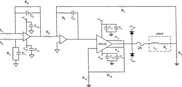
Our microcontact printing tool is a four-axis machine that enables sub-micron accuracy of motion. It employs a novel hybrid control scheme, using force and position data to control the printing. Stamping may be observed in real-time, and process data can be collected for real-time or post-stamping analysis.
As shown in Figure 1-1, the machine fixtures the substrate to be printed on a vacuum chuck. This chuck is bolted to a cast-iron surface plate, which serves as the machine frame. The top of the surface plate has been hand-scraped by the manufacturer to a flatness on the order of micrometers. This reference plane facilitates alignment of the machine components.
The stamp is carried on the bottom of the stamp head on a short-travel 3-axis stage which is supported by flexures. Three voice coil drives and three capacitance gages allow the closed-loop control of these three axes (piston, pitch, roll) to effect stamping and the control of stamp parallelism to the substrate.
The stamp head is carried on a long-travel (100 mm) stage to facilitate changing stamps and substrates. This stage rides on crossed-roller bearings, and is driven in the vertical axis by a servomotor and ball screw.
Linear Stage
Small Angle Bracket
Stamp Head Large Angle Bracket
Surface Plate
Wafer Chuck Load Counterbalance
Figure 1-2: CAD model of printing tool
The printing element is a thin stamp, integrally bonded to a rigid backing. As part of this project, we developed a scalable and robust method of manufacturing this component as well. A picture of the molding setup that we used in fabricating the stamps is shown in Figure 1-3.
The stamp is made of polydimethylsiloxane, an elastomeric material that has fa-vorable bulk material and surface properties. A master, which bears SU-8 photoresist
features on a borosilicate glass disc, is fixtured facing a second borosilicate disc. This second disc serves as the stamp backing. The discs are separated by a known gap width, and the cavity between them is filled with the elastomeric prepolymer by drawing vacuum at the top of the apparatus.
We devised a method to part the cured stamp from the master without subjecting the delicate stamp to large forces. A pressurized fluid is injected into the cavity from the top. This pressure acts on the interface of the stamp and the master, and creates a parting front that spreads across the stamp-master interface. This pressure, and
Figure 1-4: Microcontact printed patterns, silver on silicon
the increase in fluid volume in the chamber, is accomodated by an elastic preloading system that hold the stamp backing and master in place.
In this thesis, we address several of the key issues involved in the automation of microcontact printing. Control of the stamping pressure is of critical importance.
Additionally, the pressure must be uniform across the entire area of the stamp, which for our project is as large as 80 cm2. The planes of the stamp and substrate must therefore be parallel during the stamping process.
In our experiments, we patterned arrays of crosses and dots with micron-scale features. Proof-of-concept tests have been very successful, resulting in the patterns
shown in Figure 1-4.
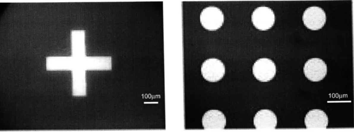
The patterns shown are silver features on a background of silicon. These are created by patterning a special ink onto a surface of silver-coated silicon. The ink acts as an ultra-thin resist, and protects patterned areas during an etching step. High resolution is achievable due to the self-assembled monolayer-forming capabilities of the ink.
The first of the images in Figure 1-4 is of a cross, with 100 micron linewidths and 500 micron cross-member lengths. The second is a dot, with a diameter of 100 microns. These features were patterned with a high degree of uniformity across a 100 mm diameter substrate.
1.2
Overview of Microcontact Printing
An enabling principle behind soft lithography is self-assembly. Through this mech-anism, molecules organize themselves in formations that are stable and orderly [61].
Of specific interest are systems in which molecules form monolayers (layers that are a
single molecule thick). These systems, known as self-assembled monolayers or SAMs, "form spontaneously by chemisorption and self-organization of functionalized, long-chain organic molecules onto the surfaces of appropriate substrates" [61].
This concept makes it possible to selectively pattern areas with a range of chemical properties, based on the type of SAM. By controlling the patterning, contiguous regions can be created with sub-micron resolution. It is in this quality that the patterning of SAMs differs from conventional printing processes. Screen printing, for
example, has a minimum resolution on the order of 20 microns [61]. Subsequent to patterning, the SAM can be used for a wide range of purposes. For example, it can act as an ultra-thin resist, to permit etching of the unprotected area. Alternatively, the SAM can be tailored to have a specific chemical or biological functionality.
Microcontact printing is a technique used to transfer micropatterns of SAMs to surfaces. The steps in this process are shown in Figure 1-5. First, a master is created
by a conventional microfabrication method such as photolithography. Following this,
a replica molding step uses a polymeric precursor to create the inverse topology, which bears microfeatures with a high degree of fidelity to the master. After a curing period, the elastomeric replica (the stamp) is separated from the master. The stamp is then inked with the SAM, and this ink is transferred to another surface through contact phenomena. A single-molecular-layer pattern is thus printed on the substrate, as defined by the contacted areas.
The elasticity of the stamp makes it possible to accomodate surface roughness while still ensuring continuity of structures and patterns. How well this contact is achieved plays a major role in the utility of the structures: uneven pressure, for example, can lead to distorted features which may be unusable. At high resolutions,
STAMP BACKING
zfl
.~
~
. ..
MASTE STAMP ASSEMBLY SUBSTRATEFigure 1-5: Microcontact printing process.
INK
F--rr3
it is thus essential to control the contact accurately.
1.3
Project Motivation
In comparison to other soft lithographic techniques like replica molding (REM) and micromolding in capillaries (MIMIC), microcontact printing is the most mature. For this reason, it is the logical choice for developing into a mass-manufacturable process. The aim of this project is to develop and demonstrate mechanisms and processes that can bring microcontact printing from the bench-scale to the prototype level. Currently, microcontact printing is carried out principally by hand. Thus, all steps from the creation of the stamp to the actual stamping are subject to variations in the technique of the practitioner.
By automating critical steps in the microcontact printing process, this variabil-ity can be limited, and we can begin research to determine such critical metrics as yield, minimum feature size, repeatability, and fidelity. Additionally, such automa-tion allows the subsequent automaautoma-tion of peripheral elements in the process, such as substrate handling and post-processing. Eventually, key metrics such as process cost and cycle time can be addressed, which will play a role in determining the commercial viability of microcontact printing.
1.4
Project Approach
Since the aim of this work is to develop a tool for further research into process, it is essential that the design is parametric. We want to be able to identify, modify, and eventually optimize each parameter that influences the microcontact printing process. Additionally, in order to limit variation due to human factors, it is necessary to automate the most sensitive process elements. Also, as a research tool, it is advanta-geous to include on-line metrology, such as visual inspection by means of microscopy.
First, the stamp generation must be carried out in a deterministic fashion, with control over the parameters of stamp material, stamp backing material, stamp thick-ness, and curing time. Additionally, the stamp backing material must have the char-acteristic of being easy to handle in a mechanized manner. The technique of casting a polymer against a previously-generated micropattern is known as replica molding. I developed an injection molding system which can readily be automated to implement this step in the process.
Second, the stamp must contact the substrate in a controlled manner. This is of great importance to ensure that even pressure is applied to the substrate surface, since this evenness will determine the fidelity of the printed pattern to the original pattern. The goal is to apply the minimum pressure required, so as to accurately replicate the pattern while accomodating any irregularities in flatness of the substrate surface. This element of the microcontact printing process is the chief focus of this thesis.
1.5
Design
The design requirements for our automated stamping apparatus are:
1. apply even pressure across a large area (a 100 mm diameter wafer)
2. allow the specification of stamping pressure
3. permit definition of the contact duration
4. provide sufficient control over environmental factors such as vibration
5. provide for subsequent automation of peripheral process elements 6. allow process observation in real-time
Additionally, the project had to be completed in about one year, within the funding limits of our sponsor.
" sensing and control of angular orientation of stamp plane relative to substrate plane
" high-resolution control of stamping force
" a flexible user interface, that permits real-time control of process parameters " mounting of apparatus on vibration-isolation platform
" long travel to allow for inking, drying, and stamp changes
" clear aperture through stamp to substrate for process observation
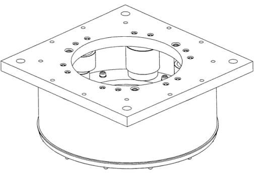
Based on these parameters we developed the machine topology shown in Figure 1-6. For the long-travel motion, we use a vertically-mounted linear ballscrew stage. To this is mounted the stamp head, which contains the high-resolution sensing and actuation elements. The transparency of the stamp and its backing makes it possible for us to view the stamping as it is taking place.
In order to achieve uniform pressure across the entire contact area, it is important that the plane of the stamp features is parallel to the plane of the substrate. For this to be possible, we need to sense the relative orientations of the two faces, and then actively pose one or both such that they are parallel. Furthermore, the planes must be parallel at the onset of contact, since SAMs begin forming instantaneously on the substrate; it is for this reason that a passive alignment means is unsuitable for micron-scale features.
Determining the relative orientation of the stamp and substrate requires knowl-edge of three discrete points on each plane. By setting one of the planes as the reference, it becomes necessary to know only three points to find the relative orien-tations. Our machine controls these linear (piston) and two angular (pitch and roll) degrees of freedom (as shown in Figure 1-6) to implement this alignment.
Coarse Translation
Piston
Roll
Pitch
Figure 1-6: Machine topology
The design we developed to address these issues is shown in Figures 1-7 and 1-8. This is a CAD model of the stamp head, which contains the alignment and
force-application elements.
Since the rotations required for alignment are small, we can use linear sensors and actuators for the fine positioning capability. A flexure provides guidance for the motion by restricting the lateral freedom of the stamp. Capacitive sensors are used to monitor position. For actuation, we use voice coils, which allow the direct control of force. When coupled with position feedback from the capacitance probes, either position or force control, or a combination of both, may be used for the stamping process. A photograph of the stamp head assembly is shown in Figure 1-9.
To fixture the stamp, it is preferable to use rigid backing to provide the reference plane, since the stamp itself is compliant. For repeatability and determinism, it is important to have a stiff coupling between the stamp and the sensor/actuator assembly. Additionally, a rigid backing serves to limit the in-plane distortions of the
Target
Voice Coil
C)
Shell Ring
Fixed Shell
Top RingCapacitance Probe
Sensor 3
Actuator C
Actuator B
Sensor 1
Sensor 2
Actuator A
FRONT
Figure 1-9: Photograph of stamp head assembly, bottom view
stamp. The choice of a material with a low coefficient of thermal expansion reduces
the stamp's thermal sensitivity as well, as the properties of the backing material will
govern the distortion of the stamp (especially if the stamp is designed to be very
thin). There must also be a method by which the stamp may be bonded to the
backing without causing any distortions of the pattern.
The material we chose for the stamp backing is borosilicate, a low CTE glass that
is economical and readily available. If tighter thermal tolerances are required, we
could use a lower-expansion substrate such as fused silica. The backing we use is 125
mm in diameter, with a thickness of 6.35 mm. The glass is polished on both sides, so
as to permit through-viewing.
A CAD model of the entire machine assembly, including the stamp head, the
linear stage, the angle irons, and the surface plate, is shown in Figure 1-10.
Although a mechanism to finely orient the stamp and substrate relative to each
other is critical, it is also important to design the machine structure to minimize the
Linear Stage
Small Angle Bracket
Large Angle Bracket
Stamp Head
Surface Plate
Wafer Chuck
Load Counterbalance
Figure 1-10: CAD model of printing tool
amount of correction that will be required. A hand-scraped cast iron surface plate is used as the base, and cast iron angle brackets are used for mounting the linear stage to the base and the stamp head to the stage. The base and angle irons have precision flat faces, and the angle-iron faces are accurately perpendicular, which ensures good alignment. The entire assembly is mounted on a vibration isolation table, which
attenuates floor vibrations.
Variation between stamps is nulled through the use of a calibration procedure. The steps of the calibration routine are shown in Figure 1-11. A representative substrate is used for this calibration, and permits the determination of the relative orientations of the stamp face and the substrate. We make the assumption that the substrate's top faces are of uniform flatness, since the wafers are thin and are held on a flat
vacuum chuck.
The calibration routine first detects the pitch and roll relative orientations by advancing the head until these feedback data are constant even as the coarse-travel
a 1) b1
b2)
b 3)
y7
Figure 1-11: Calibration procedure: al) Initial position; a2) Advance and record pose; a3) Retract, pose head, end calibration; bi) Ink stamp; b2) Contact substrate, transfer ink; b3) Retract
slide is advanced (Figure 1-11, a2). This constancy indicates that the stamp face and the substrate face are fully contacted and parallel, although there may be a high pressure at the interface. The pitch and roll position feedback data for this orientation is recorded. The stamp is then retracted from contact, and the voice coils are used in a current control mode to pose the head to the contacted orientation (Figure 1-11, a3). It is important to pose using current (force) control rather than position control, so as to prevent the addition of any stiffness to the head.
a 2)
a 3)
b 1)
After the pose is set, the stamp is again lowered toward the substrate. This time, the aim is to detect contact. A change in the piston feedback indicates that contact has been achieved. After contact, the head is advanced further, to ensure that the pose does not change. If the pose remains constant and in accord with the previously-recorded pose data, the calibration is complete. Otherwise, the routine returns to the first calibration step, of pose detection. The substrate used in the calibration step need not be a SAM-ready one, since it is used simply to provide a representative thickness and flatness. The stamp is also not inked at this phase of operation.
During the stamping step, the stamp is lowered to a position that is a predeter-mined standoff from the surface of the substrate. It is then slowly advanced toward the substrate until contact is detected again. This is necessary because at the micron scale, there is significant variation in the substrate thickness. The stamping pressure is applied by the flexure. After contact, the coarse slide is advanced by a predeter-mined distance. This distance determines the stamping force by way of the flexures'
deflection and stiffness.
The strategy for controlling the application of pressure in a uniform fashion across the entire substrate can make use of both force and position control modes. Figure 1-12 illustrates the control algorithm that we implemented to calibrate the stamp to the substrate, and to control the stamping motion.
The machine topology that we have chosen makes it possible to investigate and quantify the effects of alignment and pressure control on impression quality with a large amount of experimental flexibility. A number of modes of operation exist
by which either or both of these parameters can be controlled in different ways. For
example, by adding a position feedback component, the effective stiffness of the stamp head can be increased or decreased.
Calibration
calibration substrateadvance head
detect pose
retract head
pose head
advance head
detect contact
Inking
retract head
user inks
wait for user
Stamping
new substrateadvance head
detect contact
advance to deflect
hold contact
retract head
1.6
Stamp Generation
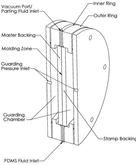
There are several key elements that are required to get from design concept to a printed, optically visible pattern. The first is the design of the pattern. For the pur-pose of rapid prototyping, a photolithographic mask may be generated by creating a high-resolution image using commercially available software such as Macromedia's FreehandTM[41. This image can then be printed with a high-resolution laser printer onto a transparency. The transparency is then used as a 1:1 contact mask to expose photoresist on the stamp substrate, in a conventional photolithographic process. This process results in a master which bears features patterned in photoresist. The raised pattern in photoresist must be the inverse of the desired printed pattern. One mod-ification to the conventional method of photolithography is our choice of substrate for the master: we use a 6.35mm thick, 125mm diameter piece of borosilicate glass, which has been coated with a thin film of gold. The gold helps to minimize internal reflection and scattering during the exposure step. Without this gold layer, the ul-traviolet light can bounce off the back side of the substrate to expose the photoresist from the backside, thereby blurring the pattern. We use borosilicate glass for the master backing material, to match the dimensional and material properties of the stamp backing, which is also borosilicate.
After the master has been fabricated, it needs to be chemically treated to be unreactive with the polymeric precursor to our elastomer, polydimethylsiloxane; a process known as silanization fulfills this requirement. This treatment ensures that the polydimethylsiloxane will not cross-link with the glass and resist surface and thus will not adhere to the master. The other glass surface, that of the stamp backing, must be treated to be reactive with the polymer, so that it will adhere to the stamp backing after these processes; this process is called plasma oxidation. The stamp will bond to the stamp backing, and part easily from the master.
Once both surfaces have been treated, they are ready for the molding, or stamp generation step. The molding scheme I designed and built is illustrated in Figure
Vacuum Port/ Inner Ring Parting Fluid Inlet
Outer Ring Master Backing Molding Zone Guarding Pressure Inlet Guarding Chamber Stamp Backing PDMS Fluid Inlet
1-13.
The two discs are fixtured with a known gap between them (we chose 100 pm) that will define the stamp thickness. This gap is set by precision shim stock, three small pieces of which are placed between the master and the stamp backing. The shim spacers are located just inside the perimeter of the glass discs, so as not to interfere with the stamp area.
To preload the discs together, we use a set of rubber blocks. Three of these are placed behind the master, and three behind the stamp backing. The preloading members are located in line with each other and the shim stock, in order to prevent undesirable deflection of the glass discs. The amount of desired preload force can be adjusted by increasing the thickness, size, or durometer of the rubber preloaders. Only a small force is required because vacuum will be drawn on the cavity; if positive pressure is being used to force the polymer in, larger preloading forces are required.
The discs are sealed at their edges with rings and oriented vertically. The o-rings are clamped axially through the bolting of the stacked assembly, and provide not only a fluidic seal but a fairly accurate locating mechanism as well.
For the molding step, the polymer precursor is pulled into the mold cavity by vacuum. It is critical at this stage to minimize the introduction of air bubbles into the mold cavity: air can be trapped within the bulk of the stamp, which can at best change material performance, or at worst destroy features. Once the precursor has filled the mold cavity to the appropriate level, the supply is shut off, and vacuum is allowed to degas the cavity. The aim of this is to remove as many of the air bubbles as possible: the viscosity of the precursor makes this a challenge.
The polymer cures in about 24 hours at room temperature. After this, the stamp is ready to be parted from the master. The connection at the top of the mold cavity, which was previously used for vacuum, is now used as an inlet for a pressurized fluid. I used a glass-barrel syringe with auto-refill capability to pump a solution of isopropanol and water through this port and into the mold cavity. The rubber
preloading members, which serve to force the discs together during the mold-filling step, now provide the required compliance to allow the fluid to part the discs. Since the rubber preloaders apply low force, the discs are able to separate at low pressure. After some pressurization, a parting line becomes visible, and propagates quickly across the interface to separate the materials. Subsequently, the assembly can be unbolted, and the stamp removed from the master. Without using a fluid-iniated parting scheme, the mechanical forces required to part the stamp from the master are very large, and can potentially cause irreparable damage to the stamp, the stamp backing, or the master. By using our fluid-parting method, the parting forces are applied by the fluid at the interface, rather than through the bulk of the stamp.
Following the parting of the stamp and its backing from the master, the stamp is cleaned and prepared for mounting in the stamp head. It is washed in ethanol and dried, and then fixtured.
1.7
Fabrication
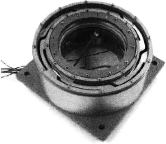
The fabrication of the elements of the machine had several steps. The first was the design and modeling of the system. I modeled the machine in SolidWorks[19]. Figure 1-14 shows the CAD model for the full assembly. After the entire assembly was designed, several of the parts requiring precision machining were sent out for manufacture. In the meantime, the machine base was prepared, and the linear stage was mounted and tested. In parallel, current control amplifiers were modified and tuned to drive the voice coil actuators, and modifications were made to a wafer chuck to customize it for this application.
After the parts for the stamp head arrived, the unit was assembled, incorporating the voice coils and the capacitance probes. This assembly is shown in Figure 1-15. I then mounted this assembly to the linear stage. During the subsequent testing of the stamp head, we found that the capacitance gages were calibrated for too short a range.
Figure 1-15: Photograph of stamp head assembly, bottom view
I recalibrated the probes and their electronics for a ±1mm range, and re-fixtured. I developed the software for the control of the linear stage in SimulinkTM[45], and
built the user interface through dSpace's ControlDeskTM software [23]. This package allows real-time tuning of the system, which proved to be an important capability: after tuning, single-micron resolution was achieved for this stage. Similar control was developed and tested for each of the voice coils, and then for the stamp head as a whole (using transformation matrices to map the actuator and sensor reference frames to a common one). Resolution of the stamp head with the recalibrated probes is on the single-micron order, but this can be improved by calibrating the probes once
Figure 1-16: Photograph of fully assembled microcontact printing tool
again to an intermediate range of ±500 microns.
An image of the fully assembled microcontact printing tool is shown in Figure
1-16.
1.8
Testing and Metrology
The main elements of the control system are the dSpace 1103 DSP board [23] (along with its associated software) and the Simulink and StateflowTh packages within Matlab [45] (a popular mathematics and modeling software). The system models are created in Simulink, and the control algorithm for the actual stamping process is modeled
in Stateflow. Stateflow is especially useful for this purpose because it constructs a state machine, which can sample the system's I/O's at a predetermined rate and cycle through a sequence of conditionally-defined states accordingly.
The user interface for the stamping allows control over the parameters of contact force via the deflection of the flexure, contact duration, and speeds of motion. The user can also view in real time the piston, pitch, and roll feedack information. For the purposes of the testing, each calibration step pauses and waits for user input to continue, but this can easily be modified to run in a fully automated fashion.
Once the calibration sequence executes successfully, the stamp is ready to be inked. For the purpose of this research, the inking is performed by hand but this step may also be easily automated to ensure even coverage across the stamp. The SAM (in solvent) is spread on the face of the stamp, and the stamp is then dried in a stream
of nitrogen gas.
Following the inking, a substrate is fixtured on the wafer chuck and vacuum is applied. The substrates used are silicon wafers, 100 mm in diameter and about 500 pm thick. They are coated with a thin film of silver (about 50 nm) via thermal evaporation, on top of an intervening adhesion promotion layer of chromium. The silver coating is used because SAMs form extremely well this metal. An additional advantage is that silver allows high-contrast imaging of the printed pattern, since after etching it is clearly visible on the dark silicon substrate. Furthermore, the etching of silver is a rapid, and therefore convenient, process.
Once the wafer is placed on the chuck, stamping may be initiated. The desired deflection of the flexure is a preset parameter. The stamp head is driven to the initial pose determined in the calibration step. The linear stage then ramps the position of the stamp head to the point of contact. This point is recorded, and the deflection proceeds from this reference. This calibration allows our algorithm to account for non-uniform thickness in the substrates.
Figure 1-17: Microcontact printed patterns, silver on silicon
retracts. At this point, the vacuum may be released and the substrate removed from the chuck. In order to see the transferred pattern optically, it is necessary to etch away the silver that is unprotected by the SAM. An etchant solution of potassium ferricyanide, potassium ferrocyanide, and sodium thiosulfate is used for this purpose. Using a wafer holder, the substrate is immersed in the etchant until the unprotected silver is etched away, and the bare silicon is visible beneath. If the SAM transfer was
successful, a clear pattern is visible.
A series of tests were performed on 100 mm wafers. Two different masters were
used, to provide metrology data for long-range and short-range characteristics of the process. One pattern contains an array of crosses, with 500 micron-long lines with
100 pm line widths, on a pitch of 1 mm. The second is an array of dots, with 100 Pm
diameters on a 200 pm pitch. The first master was made using a transparency mask, and the second with a chrome mask.
Some of the final results of the stamping are illustrated in Figure 1-17. The images are taken using an Olympus BX60 optical microscope in reflectance mode. Initial tests used a fluorescent, non-SAM ink, which permitted immediate visualization of the stamped areas. After this was determined to be satisfactory, SAM inks were used in conjunction with the etching process to determine actual performance. The features illustrated in the figure demonstrate our ability to pattern to at least 10 ,um
resolution, as evidenced by the sharpness of the cross corners.
1.9
Thesis Contributions
The chief contribution of this thesis is the development of automated methods of performing microcontact printing. As part of this effort, we designed, fabricated, and tested a device to carry out the process. Specific contributions are:
" Methods for generating stamps in a deterministic fashion, with control over
lateral distortions, thermal effects, and uniformity of thickness
" Techniques for parting a stamp from the master while minimizing tensile stresses
and irreparable distortions while using a thin stamp with a rigid backing
" Automated control of stamping pressure and uniformity of contact in
microcon-tact printing
" Strategies to detect and control the relative orientations of a compliant surface
and a rigid surface
" Successful experimental demonstration of these processes
1.10
Thesis Organization
The first chapter of this thesis gives an overview of our development and design of a device to perform microcontact printing in an automated fashion. The aim of the work is to produce accurate high-resolution patterns across a large area, specifically on the treated surface of a 100 mm silicon wafer.
Chapter 2 contains a review of the state-of-the-art in microcontact printing and related technologies. This is useful in order to put our research into the appropriate context.
Chapter 3 details the design of the microcontact printing tool and each of the key components and subassemblies. This chapter also contains relevant modeling and calculations.
Chapter 4 discusses stamp generation techniques. As the stamp is the pattern transfer element for microcontact printing, its design and fabrication are key deter-minants of maximum resolution and quality.
Fabrication issues are addressed in Chapter 5. This chapter explains the
assem-bly procedure for the printing tool, as well as the molding process for the stamp
generation.
Chapter 6 presents the development and implementation of the controls for the microcontact printing machine. This chapter also discusses the user interface.
Testing and metrology are presented in Chapter 7. Testing methodology, images, of printed patterns, and some analysis of the results are given in this chapter.
Chapter 2
Literature Review
Microfabrication is a broad and rapidly expanding field. With applications ranging from the semiconductor industry to optics to biotechnology, the potential for advances in multidisciplinary areas is immense.
Although the origins of microfabrication are in microelectronics, other fields of science and technology are making increasing use of microfabricated structures and patterns. Oftentimes, the ideal requirements for these other fields are not met due to the limitations iimposed by conventional microfabrication techniques such as pho-tolithography. For example, the silicon media and the harsh chemicals used in silicon processing make photolithography less than ideal for biological applications, since many biological elements behave very differently when in unfavorable environments.
For these reasons and others, new approaches to microfabrication are being de-veloped. One such groundbreaking technology is soft lithography.
2.1
Soft Lithography
Soft lithography is the name given to a broad suite of technologies that share the common use of soft materials for a variety of purposes. The techniques enable two-dimensional patterning in a range of materials, as well as three-two-dimensional replication
of microstructures. Furthermore, highly specialized chemistries play an important role
in widening the range of potential applications.
Two principal techniques that fall under the soft lithography umbrella are micro-contact printing and replica molding [61]. The first technique uses an elastomeric pattern-transfer element to print a monolayer of a chemical species onto a surface. The second technique replicates the inverse topology of an existing three-dimensional microstructure. When the two techniques are used in conjunction, they provide the
ability to pattern a wide range of microscale features.
One area of research that can benefit from soft lithographic processes is biotech-nology, where there is a desire to observe interactions taking place on the cellular level. The environments to which cells and other biological entities are exposed can be carefully controlled and tailored to mimic their natural environs, or modified in order to assess changes in behavior. Since biologicals are often very expensive, it is also useful to minimize the amount of chemical reagents required. For these rea-sons, soft lithographic fabrication can prove useful, since it permits the generation of microstructures and surfaces with easily modifiable chemistries.
An application example in the biotechnology area is in the patterning of assays. These are micro-array devices that consists of patterned proteins. By creating well-defined patterns of proteins, detection capability is improved, and larger amounts of data may be extracted. Soft lithographic process using microfluidic networks and mi-crocontact printing enable protein patterning because by incorporating soft materials, they are able to preserve biological activity [6].
Another area for which soft lithography has proven useful is in optics. The use of an elastomeric pattern-transfer element makes it possible to print microfeatures onto curved surfaces [51], and the use of replica molding permits the fabrication of lenses or fiber optics bearing integral microfeatures. When combined with plating processes, three-dimensional structures such as coils may be created for use as elements in mi-croelectromechanical systems (MEMS) [50].