spin polarized light transport in magnetized noncentrosymmetric 1D
photonic crystals, and photonic gaps and fabrication
of
quasiperiodic
structured materials from interference lithography.
by
Ion Bita
B .Sc. Chemical Engineering, B.Sc. Chemistry Massachusetts Institute of Technology, 2000
Submitted to the Department of Materials Science and Engineering in Partial Fulfillment of the Requirements for the Degree of
Doctor of Philosophy in Polymers February 2006
O Massachusetts Institute of Technology
1
LIBRARIES
1
Signature of Author:
...
. . .-
Department of Materials Science and EngineeringFebruary 6,2006
...
.
..
.
.
...
Certified by: .Y.w
-.
.- w C.w.Edwin L. Thomas Morris Cohen Professor of Materials Science and Engineering Thesis Advisor
n
A
-
w - - - dAccepted by:
...
.;/'
.
v.-....
Samuel M. Allen POSCO Professor of Physical Metallurgy Chair, Departmental Committee on Graduate Students
crystals, and photonic gaps and fabrication of quasiperiodic structured materials from interference lithography.
by Ion Bita
Submitted to the Department of Materials Science and Engineering on February 6,2006 in Partial Fulfillment of the Requirements for the Degree of
Doctor of Philosophy in Polymers
Abstract:
Effects of breaking various symmetries on optical properties in ordered materials have been studied. Photonic crystals lacking space-inversion and time-reversal symmetries were shown to display nonreciprocal dispersion relations, and to exhibit a remarkable set of symmetry-related properties. Even in ID, these materials are found to display indirect photonic band gaps, backward wave propagating modes (antiparallel phase and group velocities) which enable negative refraction at the air-crystal interface, ability to allow bending light with perpendicular magnetic fields, unidirectional superprism effects, etc. By calculating the complex photonic band structure, we show that the gap modes differ fhdamentally fkom the commonly assumed evanescent modes with purely imaginary wave vectors
-
solely due to symmetry, we show that the gaps of nonreciprocal photonic crystals have complex wave vectors with both imaginary components and non-zero, frequency dependent real components. This basic finding is further studied in the context of tunneling dynamics, by considering the problem of tunneling time for nonreciprocal photonic band gap barriers (the tunneling wave packet has an energy in the middle of the gap). It was found that the classical Hartman effect (independence of tunneling time on barrier length, beyond a certain length), previously implied as universal, is forbidden solely due to symmetry. Instead of a classical zero group delay, we find that tunneling wave packets with opposite spins display non-zero group delays, with opposite signs. Due to analogies based on symmetry, these results directly impact the problem of spin- polarized electronic tunneling in magnetized noncentrosymmetric semiconductors, such as GaMnAs or carbon nanotubes with applied axial magnetic fields.An interference lithography based fabrication process was developed to produce 2D and 3D quasiperiodically structured materials, which have long-range order but break translational symmetry. Multiple exposure interference lithography was used to fabricate 2D quasicrystals with feature sizes as small as 100nrn. Replica molding was used to fabricate transparent and conformable 2D quasiperiodic phase masks, which subsequently allowed the fabrication of 3D structured materials with quasiperiodicity by coherent diffiraction lithography. The effect of the higher point group symmetries of 2D quasicrystals on photonic band gap formation (TM polarized only) was studied by finite difference time domain calculations, and it was found that increasing the rotational symmetry does not always lead to wider gaps.
Thesis supervisor: Edwin L. Thomas
Chapter 1
-
Thesis overviewChapter 2
-
Introduction to photonic crystals2.1. The basics
2.2. Photonic crystals as semiconductors for light 2.3. Optical properties of photonic crystals 2.4. Conclusions
2.5. References
Chapter 3
-
Light propagation in photonic crystals breaking space-inversion and time-reversal symmetries3.1. Introduction
3.2. Constitutive Relations
3.3. Electrodynamics of homogeneous media without time-reversal and time-inversion symmetries 3.4. Axial wave propagation: analytic dispersion relation
3.5. Arbitrary wave propagation: numerical modeling with the transfer matrix method 3.5.1. Bloch Solutions in M i t e 1D Periodic MO-HM Photonic Crystals
3.5.2. Reflection and Transmission Coefficients of a Finite Thickness 1D Periodic MO-HM 3.6. Effect of magnetooptic activity on the photonic band structure of 1D periodic helical media
3.6.1. Photonic Band Structure of 1D Periodic MO-HM with g((q
3.6.2. Photonic Band Structure of 1D Periodic MO-HM with g l q
3.7. Conclusions 3.8. References
Chapter 4
-
Tunneling time for barriers lacking space-inversion and time-reversal symmetries4.1. Introduction
4.2. Gap states in nonreciprocal photonic crystals
4.3. Tunneling phase time in nonreciprocal photonic barriers 4.4. Results
4.5. Conclusions 4.6. References
Chapter 5
-
Photonic band gaps in 2D quasicrystals5.1. Introduction
5.2. Quasiperiodic structures in 2D
5.2.1. Quasiperiodic 2D structures from interference lithography (IL) 5.2.2. Quasiperiodic 2D structures from quasiperiodic tilings
5.3. FDTD for computing photonic band gap frequencies
5.4. Effect of point group symmetry on PBG formation in IL-PQC 5.4.1. Effect of symmetry on 2D TM PBG formation in 2D PC 5.4.2. Effect of symmetry on 2D TM PBG formation in 2D IL-PQC 5.5. Comparison of PBG formation in IL-PQC and PROJ-PQC
5.6. Summary and Conclusions 5.7. Future Directions
5.8. References
Chapter 6
-
Fabrication and applications of 2D and 3D quasiperiodic sub-micron structured materials from interference lithography6.1. Introduction
6.2. Quasiperiodicity and IL: theoretical problems
6.2.1. Theoretical comparison of multiple beams IL vs multiple exposures IL for 2D PQC fabrication
6.2.2. Minimum number of beams (or exposures) for 2D quasiperiodicity 6.2.3. Theoretical model for interference lithography in 3D
6.3.2. The Lloyd's mirror lithographic interferometer
6.3.3.2D QPC fabrication issues: contrast in Multiple Exposure IL 6.3.4. Fabrication process: the tri-layer resist process and materials 6.3.5. Results
6.4. Towards Applications
6.4.1. Fabrication of quasiperiodically structured 3D materials by coherent diffraction lithography with 2D quasiperiodic transparent phase masks
6.4.2. Self-Assembly of block copolymers thin films on 2D quasiperiodic topographically patterned substrates
6.5. Conclusions 6.6. References
Chapter 7
-
Thesis conclusions and future directions7.1. Overview of research accomplishments 7.2. Future research directions
Figure 2-1 - Examples of 3D photonic crystals. (a) Face centered cubic crystals obtained by sedimentation of colloidal silica particles [I]; (b) Self-assembled double gyroid crystal from a polystyrene- polyisoprene diblock copolymer after the isoprene phase was selectively removed [2]; (c)
"Woodpile" photonic crystal fabricated in silicon [3]; (d) Simple cubic lattice photonic crystal made in silicon [4].
Figure 2-2
-
Analogies between atomic crystals and photonic crystals. Adapted from [I 11. See text.Figure 2-3
-
1D photonic crystal with a bilayer unit cell.Figure 2-4
-
(a) Dispersion relation in a 1D photonic crystal showing formation of the first band gap andpropagating modes in the photonic crystal (solid lines). Dashed lines represent the solutions in the case of a homogeneous material, the limit of equal dielectric constants in the two layers of the photonic crystal unit cell. (b) Definitions of the phase and group velocities. A wave packet (or pulse) is shown in order to emphasize that the phase velocity corresponds to the motion of phase fronts, while the group velocity gives the signal velocity, the velocity with which the pulse envelope propagates in space.
Figure 2-5
-
(a) Periodic dispersion relation solution for a 1D photonic crystal. The gray area indicates thereduced Brillouin zone. (b) Band structure of a 1D photonic crystal obtained either by folding the w(k,) solution belonging to k,=O into the reduced Brillouin zone, or by generating the upper bands using the periodicity of the dispersion relation, as shown in (a).
Figure 2-6
-
Calculated photonic band structures for 1D photonic crystals with bilayer unit cells and nl = 1.5, and n2 = 2.2. (a) Photonic gaps form at all band crossing points in the case when the layers have the same thickness, dl = d?, similar to the conceptual diagram shown in Figure 2-6; (b) In the specialcase when the optical thickness of each layer is a constant (also called quarter-wave case) certain photonic bands remain degenerate instead of forming gaps.
Figure 3-1
-
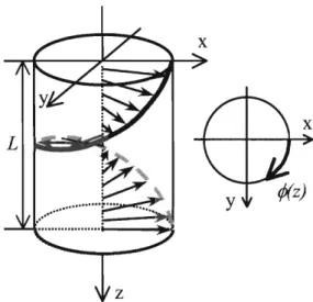
Conceptual representation of the structural rotation throughout the unit cell of a 1D chiral photonic crystal showing the periodic, right-handed (RH) continuous twist along the z axis of an arbitrary vector with fixed orientation in the local material coordinate system. The spatial period L is defined for a fill 2.n rotation, +(z+L) = +(z) + 2.n.Figure 3-2
-
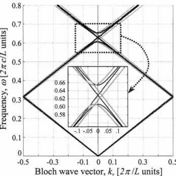
Numerically calculated photonic band structure for axial propagation, w(k,, kx=k,,=O), at two orientations of the magnetogyration vector, gJlz (gray curves), and gllx (black curves). Inset shows a magnification of the photonic band structure near the bandgap. Note that the gJJx band structure is also valid for the case when no magnetooptic activity is present, describing a simple dielectric helical medium.Figure 3-3
-
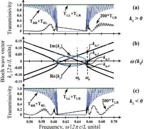
(b) Numerically calculated photonic band structure for axial propagation, dk,, kx=ky=O),through a finite piece of the RH photonic crystal, showing the total transmissivities of LCP waves (TLL+TLR) and stop-band for RCP waves (TRR+TRL). The polarization conversion contribution (TLR=TRL) is scaled by a factor of 200, for visibility on the same plot; (c) same as (a), but the magnetogyration vector is reversed (y < 0), corresponding to an incident wave propagating in the -z direction.
Figure 3-4 - Isofiequency sections through numerically calculated dispersion surfaces, cll(k&=O,k,); (a) Effect of magnetooptic activity (y > 0) on the isofrequency contours, when w = 0.65 [2zc/L] and the magnetogyration vector is parallel to the helical axis (gllz) ; (b) Isofiequency cuts at multiple frequencies, for constant magnetooptic activity (y = 0. I, gllz).
Figure 3-5 - Isofiequency cut at w = 0.67 [2nc/L] through numerically calculated dispersion surfaces, ajk,ky=O,kz), when gllz (y =O.I), showing the directions of the Poynting vectors of four eigenrnodes that are phase matched to a particular value of the parallel wave vector, k,.
Figure 3-6 - Isofiequency cuts through numerically calculated dispersion surfaces, w(kvk+=O,kz); (a) Effect of magnetooptic activity (y > 0) on the w = 0.65 [2z c/L] contours, when the magnetogyration vector is perpendicular to the helical axis (gllx) ; (b) Isofiequency cuts at multiple frequencies, for constant magnetooptic activity (y = 0.2, to exaggerate this qualitative effect, gllx).
Figure 3-7
-
Isofiequency cut at w = 0.65 [2z/L] through numerically calculated dispersion surfaces, cll(k,k+=O,kz), showing three different regimes of transmission when gllx ( y = 0.2 to exaggerate the effect graphically); (i) and (iii) depict normal refiaction at the air-photonic crystal interface; (ii) shows negative refiaction at the air-photonic crystal interface.Figure 4-1
-
(a) dPBG at the anticrossing of bands with equal group velocities; (b) iPBG at the anticrossing of different vg bands, as seen in nonreciprocal PCs. The original bands are shown with dashed lines, the coupled propagating modes with solid, black curves and the expected real part of the gap modes with a thicker solid gray line.Figure 4-2 - (a) Reciprocal band structure with dPBG for a 1D PC breaking only T-R symmetry (EF = 1.72, y~ = 0. I, E, = 1.52,
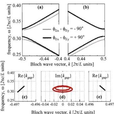
4
= 0 in Eqs. (2) and (3), see text); (b), (c) and (e) Magnification of the first gap region showing the original bands and the real and imaginary parts of the complex kgap solutions in the PBGs - note the vertical alignment at the edge of the first Brillouin zone.Figure 4-3 - (a), (b) Nonreciprocal band structure for a 1D PC breaking both S-I and T-R ( E ~ = 1.72, y~ = 0.1, E, = 1.52, & = 0.02 in Eqs. (2) and (3), see text). (c), (d) and (e) show the gap mode solutions. Note the vertical (mirror) symmetry about k = 0 of Im(kgap) solutions and the different frequency dependence of the Re {kgap) solutions.
Figure 4-4 - Tunneling time for RCP and LCP pulses with narrow frequency bandwidths centered in the gaps of the LCP and RCP bands shown in Fig. 4-2 (dPBG) and Fig. 4-3 (iPBG). In both cases the
Figure 5-1 - Quasicrystalline structures. (a) HRTEM phase-contrast atomic-resolution image of
Zn6Mg3Ho decagonal quasicrystal viewed along the 10-fold rotation axis [www.jeol.com] and a
photograph of a macroscopic (rnm scale) quasicrystal; (b) and (c) SEM pictures of photonic quasicrystal made by etching holes in a pattern given by a quasiperiodic tiling - Penrose in (b) (from [12]) and dodecagonal in (c) (from [13]); (d) and (e) calculated quasiperiodic light intensity patterns from interference of laser beams, showing 10- fold and 12-fold rotational symmetries (this work).
Figure 5-2
-
Spatial distribution of the total light intensity, I(x,y), pattern for (a) square crystal (N = 2 exposures); (b) octagonal (N=4), (c) decagonal (N=5) and (d) dodecagonal (N=6) quasicrystals. The axes units are normalized to the laser wavelength, and higher intensities are plotted as lighter pixels.Figure 5-3 - Quasicrystalline structures with 18% fraction of a given component (white pixels) for the investigated rotational symmetries; the (X-1) series corresponds to I > ,,I, while the (X-2) series to I
< I, (X = a, b, c); (a) octagonal quasicrystal with IcuiImmimm = 67% in (a-1) and 33% in (a-2); (b) decagonal quasicrystal with Icu{Imarimum = 63% in (b-1) and 34% in (b-2); (c) dodecagonal quasicrystal with Icu{Immimum = 64% in (c-1) and 35% in (c-2).
Figure 5-4 - (a) Octagonal, (b) decagonal, and (c) dodecagonal patterns with varying volume fractions of
the white region (where I(xy) > ),,,I, showing not only a continuous change of the size and shape of particular features, but also a discontinuous appearance of new structural features. Values of the corresponding I,,, are given in Table 5-1.
Figure 5-5
-
Generation of a 1D quasicrystal by projection from a 2D square lattice. The key requirement is for the (e.g. ID) axis E (onto which the projection is done) to be oriented at an irrational angle with respect to the translation vectors of the higher dimension (e.g. 2D) periodic structure. Adapted from 11 11.Figure 5-6 - Examples of 2D quasicrystalline tilings. (a) octagonal quasicrystal; (b) decagonal quasicrystal and (c) dodecagonal quasicrystal. The patterns are centered with the high rotation axis at (53).
Figure 5-7
-
18% fill fraction 2D quasiperiodic structures based on mathematical quasicrystalline tilings (for comparison with interference lithography structures shown in Figure 5-3).Figure 5-8
-
Comparison between the location of the PBG via (a) photonic band structure (exact method), and (b) FDTD calculation of the LDOS at the center of a dielectric cylinder (approximate method) for a 2D triangular lattice with 10% dielectric rods with E = 6 in air.Figure 5-9
-
Width of the 1st TM PBG in square and triangular 2D photonic crystals as a fhction of volume fraction, for dielectric (a) E = 4, (b) E = 6, (c) E = 8, and (d) E = 11.4 cylindrical rods surrounded by air. Each point on the plots represents an actual band structure calculation.Figure 5-10 - Gap maps from assembling the LDOS curves calculated at the point (0,O) in each shown structure, for fill fractions f = 0.05-0.16 (steps of 0.01), and 0.18-0.30 (steps of 0.02) for (a)
regions) are shown above each LDOS plot for emphasizing the structural differences between quasicrystals. Note that a = &ntederen,J2 = 1.
Figure 5-11
-
same as Figure 5- 10, but with E = 8 for the dielectric component (higher dielectric contrast).Figure 5-12
-
Gap maps from assembling the LDOS curves calculated at the highest point group symmetry location in each structure at various fill fractions for (a) 2D triangular photonic crystal, (b) octagonal PROJ- PQC and (c) octagonal IL-PQC, all with E = 4 dielectric in air. Small pieces of each PBG structure with 18% dielectric (white regions) are shown above each LDOS plot for emphasizing the structural differences between quasicrystals.Figure 5-13
-
same as Figure 5-12, but for a dielectric with E = 6.Figure 5-14
-
Gap maps from assembling the LDOS curves calculated at various fill fractions for (a-1) IL- style and (a-2) PROJ-style 2D decagonal quasicrystal, and (b-1) IL-style and (b-2) PROJ-style 2D dodecagonal quasicrystal, all with E = 6 dielectric and air. Small pieces of each PQC with 18% dielectric (white regions) are shown next to each LDOS plot for emphasizing the structural differences between quasicrystals.Figure 5-15
-
Same as Figure 5-14, with E = 8 dielectric and air.Figure 5-16 - Effect of a shift of the projecting plane in high dimensions. The projected Penrose-family 2D quasicrystalline structural changes. (a) projection plane going the origin of the higher dimensional space, (b) shift with half a period in the hyperspace. See [ l 11.
Figure 6-1 - IL with 5 beams arranged to produce a Penrose-like quasicrystal. (a) orientation of the k vectors corresponding to each beam; (b) orientation and relations between the difference vectors,
A&/, that correspond to the pair-wise interference of any two of the 5 beams shown in (a).
Figure 6-2 - Perspective and top-down views of the 2D decagonal QC intensity distributions obtained from IL with (a) 5 exposures with 72' rotations and (b) 5 beams separated by 72". In all cases, the axes are in units of the wavelength, h = 1, and the polarizations are out-of-plane and in phase.
Figure 6-3 - 2D quasiperiodic pattern obtained from 3 exposures of line gratings with equal spatial periods (P = hl2 = 0.5, see Eq. 6-I), but oriented as shown in the inset figure (at 0°, 36' and 90" measured from x towards y). (a) Total intensity pattern; (b) Binarized intensity pattern obtained by thresholding at Ithreshoki = 75% I,,,, = 9; (c) horizontal profile at y = 0 for the total intensity pattern shown in (a); (d) horizontal profile at y = 0 for the binarized intensity pattern shown in (b). All dimensions are in units of h.
Figure 6-4
-
(a) A laser beam propagating in the xyz lab coordinate frame in an arbitrary direction k, with arbitrary amplitude and polarization given by E l and EZ; (b) Defnition the elezej coordinate system in relation with the xyz coordinate system.vectors in the sample plane are separated by 72'); (b) Five exposures of line gratings formed by IL with 2 beams, where the sample substrate is rotated with 72' after each exposure.
Figure 6-6
-
(a) Configuration of the Lloyd's mirror IL system built and shared by the MIT Nanostructures Laboratory; (b) Sample holder assembly, showing the rotation axis for changing the grating periodicity, and the axis around which the substrate is rotated during ME-IL; (c) Rotating the entire stage assembly changes the incidence angle and thus the periodicity of the recorded gratings. Adapted from [29].Figure 6-7
-
Dependence of volume fractions on the intensity cutoff level for 2D quasiperiodic patterns obtained from 4, 5, and 6 exposure IL. Representative pictures of the three types of 2D PQC structures at a few fill fractions are also shown in Figure 5.4.Figure 6-8
-
Tri-layer resist stack. An optically absorbing antireflection coating (ARC) placed on top of the substrate is used to eliminate the reflection R2 from the bottom of the photoresist layer, such that only the interference between the TI rays is recorded. An optically thin interlayer (e.g. 20nm Si02) is placed between the photoresist and ARC layers for accurately capturing the photoresist pattern before transfer into the substrate.Figure 6-9
-
Process flow for using ME-IL to fabricate 2D PQC samples, with SEM images of actual samples produced in the case of line gratings (one exposure). (a) the initial tri-layer resist stack is composed of 200nm photoresist, 20nm Si02 and 200nm organic ARC material, on a 1.5pm thermal oxide coated silicon wafer substrate; (b) the developed photoresist structure; (c) the Si02 interlayer is etched with CHF3 RIE using the photoresist as a mask; (d) the pattern is M e r transferred into ARC by etching with O2 RIE using the thin Si02 caps as a mask; (e) the 2D quasiperiodic pattern is finally transferred to the Si02 substrate by CHF3 etching using the ARC as a mask; (f) the final 2D PQC sample is obtained by stripping the ARC mask with 0 2 plasma.Figure 6-10
-
(a) Tri-layer resist stack structure: (from the top) photoresist, Si02 interlayer, ARC layer and substrate (1.5pm thermal oxide on silicon); (b) Effect of varying the thickness of the ARC layer on the reflectivity R2 h m the bottom interface of the photoresist layer in the case of a 300nm period grating. The simulations used the refractive index data provided in Table 6-2.Figure 6-11
-
Scanning electron microscope images at 30k magnification of Si02 line gratings obtained from photoresist patterns produced using two IL approaches. In (a) and (b) a single exposure of 11.751ni.n (1 15nW laser power delivered at the sample plane) is performed. The same total dose is delivered in (c) as 4 exposures and in (d) as 5 exposures, but additional lmin delays are introduced between each exposure. It can be seen that the resulting gratings are virtually identical within the error limit of the SEM measurement. Measured duty cycles are 43% in (a), and 41% in (b), 39% in (c), and 41% in (d).Si02. Areas with local 5 and 10 fold rotational symmetries are emphasized, and a portion of a Penrose tiling pattern is overlayed on the sample image. The inset figure shows an edge-on SEM image of the same sample, where the height of the posts is 240nm. The structure was obtained by 5 exposures with 36' rotations of 300nm period line gratings.
Figure 6-13
-
Top-down SEM images of 2D (a) octagonal, (b) decagonal, and (c) dodecagonal quasiperiodic structures in silica produced by ME-IL with N = 4, 5, and 6, respectively, exposures and rotations with 180°1N angles. Views of the central axis showing 8mm, 10- and 12mm point symmetry.Figure 6-14
-
Effect of exposure dose on the recorded photoresist pattern for the case of a 2D decagonal quasicrystal from ME-IL with 5 exposures and rotations with 36'. The fiaction of substrate area covered with photoresist (gray areas in the figures) is 66% in (a), 44% in (b), and 30% in (c).Figure 6-15
-
Comparison between SEM images of experimental photoresist patterns produced by ME-IL with (a) 5 exposures and 36' rotations, or (c) 6 exposures and 30" rotations, with computed intensity patterns approximating the experimental conditions, as (b) and (d). 300nm period line gratings were recorded in each exposure.Figure 6-16
-
Large area, plan view SEM image of an octagonal 2D quasiperiodic silica structure obtained by 4 exposures of line gratings with 300nm periodicity, and subsequent rotations with 45'.Figure 6-17
-
Coherent diffraction lithography (also known as phase mask lithography). The schematic shows an implementation for creating 3D nanostructured polymeric templates by recording the near field intensity pattern generated by an elastomeric, transparent, 2D periodic diffraction grating into a photoresist. From [40].Figure 6-18
-
(a) Elastomeric replica in PDMS of an octagonal 2D quasiperiodic silica grating. The depth of the topographical features is 4 5 k , (b) the difiaction spectrum obtained for a 632nm HeNe laser - imaged by projection on a paper screen placed at 5.2cm away from the PDMS grating (digital photograph captured by Mr. Marcus Dahlem, MIT EECS).Figure 6-19
-
A sub-micron structured, 3D epoxy polymeric network with quasiperiodicy obtained by CDLwith a transparent octagonal 2D quasiperiodic PDMS grating, exposed with the 361nm line of an Ar- ion laser. Representative local octagonally symmetric regions are indicated with green octagons.
Figure 6-20
-
(a) Schematic of a diblock copolymer molecule, formed by two chemically distinct polymer chains joined covalently. Polystyrene-b-polyisoprene is shown as an examle; (b) Bulk morphologies obtained in diblock copolymers as the volume fraction of a component is increased from 0 to 50%.Figure 6-21
-
Block copolymer nanolithography. Formation of a nanopatterning mask after selectively removing a component from a self-assembled block copolymer thin film with either spherical or cylindrical morphology.Figure 6-22
-
Plan view SEM images of representative 2D quasiperiodic array of posts used as templates for BCP self-assembly studies (a) 2D dodecagonal QC; (b) 2D octagonal QC.assembled on 2D quasiperiodic topographically patterned substrates with 12-fold rotationally symmetric QC and (b) 8-fold rotationally symmetric QC.
Figure 6-24
-
MIT Nanoruler Project: 12" wafer patterned with 400nm period line gratings (http://web.mit. edu/newso~ce/2004/nanoruler-0128. html)Table 5-1 - Values of Ic,, and corresponding dielectric volume fractions of 2D quasicrystals from IL where dielectric material is generated in regions with I(x,y) > I,,,, see Figure 5-4.
Table 5-2
-
Effect of dielectric cylinder radius on volume fraction in 2D PQC obtained from 2D quasiperiodic tilings as shown in Figure 5-7, calculated for a square sample of side 21a discretized with 32pointsla (a = 1, same sizes as used in the PBG simulations discussed in Section 5.3). For each symmetry, we also include the total number of cylinders contained in the 2 1x2 1 a computational box.Table 5-3 - 2D TM PBG results from LDOS calculations at the center of high point group symmetry, for 2D square (4mm) and triangular (6mm) PC, and 2D 8mm, lOmm, and 12mm IL-PQC and, respectively, PROJ-PQC. The results correspond to a dielectric contrast of 8:1, at the fill fraction of
15%, where the 2D PC have maximum PBG widths.
Table 6-1 - Analysis of the uniqueness of the 10 general wave vector differences in Eq. (6-6) for the case of an equiangular spacing of the five beams (72" angle). The data in this table relates to Figure 6-1. Table 6-2 - Materials, deposition techniques and their refractive indices used in the tri-layer process
outlined in Figure 6-9 (list in order of deposition).
I am writing this section last, in the early morning hours of the day following my PhD defense. I am not sure I will be able to fully capture in words the gratitude I feel for the life enriching experiences I have enjoyed throughout the past nine years while here at MIT, as an undergraduate of Courses 10 and 5 between 1997-2000, and then as a graduate student in Course 3.
This section would not feel just without first acknowledging the mentorship of a few people from my undergraduate years, which have significantly shaped my later path at MIT. In particular, I am very thankful to Prof. Timothy Swager of the Chemistry Department for having offered me a place in his laboratory and my first real research job. Tim is an incredible scientist, and I feel fortunate for having been part of his lab. It was during the two years I spent working with him that my interest in the optical properties of materials has crystallized and ultimately led to my decision to join the PhD program of the DMSE at MIT. I am also very thankful to Prof. Robert Cohen of the ChemE Department, who was the first to teach me about polymer physics and offer genuine altruistic mentorship outside the classroom. I remember vividly the many conversations we had about graduate school and in particular about my desire to enroll in the ChemE Practice School. Bob is a wonderful individual, who cares deeply about the well being of his students. Last, but not least, I would like to acknowledge the late Dr. Michael Mohr, my undergraduate advisor. Mike remains to me the epitome of what a true Chemical Engineer is, and a reason for which I feel proud for still having some ChemE blood running through my veins. His passing away last year was a great loss for all of us that knew him.
Among all at MIT, I am most grateful to Prof. Edwin Thomas, my PhD advisor. From all my mentors, Ned has been by far the most influential contribution to my academic development. I feel very fortunate for having worked with, and learned from Ned on so many occasions, and am very thankful for his continued support throughout the past years as my research grew out of the initial mold it was supposed to fill. Ned's personal example remains to me the standard for an insatiable appetite for good science,
success of his students. His unwavering support, and insightll feedback has allowed my research to truly bloom, and to reach boundaries that I could not have imagined when I joined his lab and the MIT DMSE.
I would also like to acknowledge the support of Prof. Henry Smith, who welcomed me in the Nanostructures Laboratory and made possible a significant portion of the research conducted in this thesis. Furthermore, I would like to thank my thesis committee, Profs. Caroline Ross, Moungi Bawendi and Rajeev Ram for their help and feedback on my research. In particular, I am thankll to Rajeev for being one of the best teachers I have ever had.
I have been fortunate over the past years to call myself the colleague and fiend of numerous people at MIT. Apologizing in advance to those that may not have been remembered at this early morning hour, I would like to acknowledge Vance Williams, Jinsang Kim, Chinedum Osuji, Chaitanya Ullal, Augustine Urbas, JongSeung Yoon, Sam Ha, Tae yi Choi, Ji Woong Park, Taras Gorishnyy
,
Rafal Mickiewicz, Joe W alish, Michael Walsh, Tim Savas, Joel Yang, Brian Cord, Jim Daley, Joy Cheng, Mihai Ibanescu, Marcus Dahlem, Joe Tracy, Dmitry Dinega. I thank you all.Among all, I am most thankll to my family. I thank my parents and brother for their continued love and support. I thank my wife Cristina for her love, patience and for believing in me, despite the long hours MIT took fiom our time spent together. I am most fortunate for having her besides me, and carry the deepest admiration for her inner strength and beauty. I am thankful to her for having given me a most beautill present four months ago, our first-born son.
Chapter 1.
Thesis overview
The central theme of this thesis has been the study of photonic band gap materials where certain symmetries are broken by design. The first half of the thesis focuses on a theoretical analysis of the basic features of light propagation and tunneling dynamics in
1D photonic crystals simultaneously lacking time-reversal and space-inversion symmetries, the photonic analogs of noncentrosymmetric magnetic semiconductors. In
the second part of the thesis, both theoretical and experimental results are reported for 2D
photonic quasicrystals, a novel class of materials where translational symmetry is broken. Chapter 2 serves as an introduction to photonic crystals (PC), structured materials with a periodic spatial variation of the refractive index on the scale of the wavelength of light [I]. Since the first part of the thesis deals with fairly advanced theoretical problems in PC physics, we set out to provide in this chapter an overview of the basic concepts and tools used to understand the optical properties of PC. The material science perspective is first adopted, and pictorial examples of real PC materials are shown. We then adopt a physics view, and by considering the case of a 1D photonic crystal, we introduce Maxwell's equations and their solutions in periodic media. A strong emphasis is placed on the fundamental connections between PC physics and the physics of electronic wave propagation in atomic crystals. Dispersion relations and photonic band diagrams are introduced semiquantitatively, and their use for predicting PC properties is described.
Chapter 3 is the first of two chapters presenting the results of our theoretical investigations of light propagation in 1D periodic PC simultaneously lacking space- inversion (S-I) and time-reversal (T-R) symmetries. S-I symmetry is absent, for example, in PC having a noncentrosyrnmetric arrangement of their material constituents (e.g. helical, or spiral dielectric structures, the case investigated in Chapter 3), or in PC comprised of noncentros ymmetric material components (i. e. optically active materials, see Chapter 4). Similarly, including magneto-optically active material components in the unit cell can break T-R symmetry if the light propagation direction is not perpendicular to the material magnetization. The representative material systems that were studied are a 1D periodic, dielectric helical medium with magnetooptic activity in Chapter 3, and a 1D periodic photonic crystal comprised of alternating layers with optical activity and with magnetooptic activity in Chapter 4.
The initial motivation for this work has been our interest in understanding the physics of PC with nonreciprocal dispersion relations, o(k) # a(-k). While the vast
majority of PC literature focuses on reciprocal systems, a 2001 publication by Figotin and Vitebsky [2] were first to report that nonreciprocal PC exhibit properties that significantly deviate from known optical properties. Figotin discussed the design of a 1D nonreciprocal PC that allows "freezing" light in one direction, while allowing free propagation in the opposite direction (an optical diode-like behavior enabled by introducing a mode with zero group velocity and zero group velocity dispersion at a fkequenc y for which the opposite propagation direction displays a normal propagating mode). In Chapter 3 we present a first comprehensive study of the optical properties of
remarkable PC properties as a sole consequence of symmetries, properties which are thus independent of the choice of materials, magnitudes of their optical constants, etc.. We introduced the concept of indirect photonic band gaps (edges not aligned in k-space even in ID, formed at the anticrossing of bands with different group velocities), and showed for the first time that 1D nonreciprocal PC will always display propagating eigenmodes with a negative group velocity in select frequency intervals (which is found to also allow for negative refraction at the air-PC interface). Furthermore, we show that the path of light inside such PC can be bent with perpendicular magnetic fields, similarly to the photonic Hall effect observed in uniform (i.e. non-periodic) materials with similar symmetries [3], and point out the presence of unidirectional superprism effects (large
variations of the refraction angle for small changes of the incident angle or of the wavelength, but only for one direction, while normal refractive properties are displayed if the propagation direction or the material magnetization are reversed). These results are remarkable, since they arise as a consequence of symmetry, and because they extend our knowledge of optical properties and phenomena enabled by PC through the carell choice of material components and their arrangement inside the unit cell.
During our studies of 1D PC breaking both S-I and T-R symmetries, we became increasingly aware of, and very interested in the consequences of the fact that optical properties arising solely from symmetry constraints should also apply in the electronic case, where the material periodicity is at the atomic scale. The electronic analog to our photonic crystal system is a noncentrosymmetric periodic atomic system containing, for example, magnetic atoms. Two prominent examples that fit this description are semiconductors with zinc-blende crystal structure (GaAs, CdTe, etc.) doped with
magnetic atoms (Mn in most cases) [4], and chiral carbon nanotubes in the presence of magnetic fields applied axially [ 5 ] . Both these types of materials are subjects of intense investigation in the fields of spin electronics (spintronics) [6]. Thus, by using this photonic-electronic crystal analogy, we were able to bring to light some unique insights into the basic tunneling electronic properties of two very important classes of materials.
Chapter 4 presents results from our investigations of the tunneling time problem in the case of spin-polarized particles traversing a barrier region lacking both S-I and T-R symmetries. The basic analysis of tunneling dynamics is conducted in the context of wave packets propagating across a barrier, which is used to describe both electronic and photonic tunneling due to analogies between Schrodinger's and Maxwell's equations [7,
81. Even though tunneling is a classical problem that has been investigated for many
decades, it remains presently an active subject for investigation, and a source of controversy (related primarily to explaining predicted and experimentally measured superlurninal group delays). While studying the band structures of our nonreciprocal 1D PC systems, it became clear to us that the classical features of tunneling dynamics cannot be exhibited in the absence of the two inversion symmetries. We find that the non- propagating, complex eigenmodes in the first photonic band gap are circularly polarized (analogous to spin-polarized electronic states), and that the gap eigenmodes are not described by the expected evanescent solutions (purely imaginary wave vector). Due to symmetry, the gap modes are shown to have complex wave vectors, with fkequency dependent and non-zero real components. This allowed us to show for the first time that symmetries alone forbid the universally assumed Hartman effect (independence of tunneling time on barrier length beyond a certain length) [7, 91. Instead, we find that, as
the barrier length is increased beyond a threshold, the tunneling time becomes linearly dependent on barrier length, and, moreover, that the sign of the group delay changes with the spin of the tunneling particle (i.e. the tunneling time can decrease with increasing barrier length). As will be discussed in Chapter 4, this unusual prediction of a negative group delay has been recently confirmed by an independent study of electronic tunneling in barriers of noncentrosyrnmetic semiconductors with out-of-plane magnetization (Znl. ,Mn,Se and Cdl,MnXTe), which are electronic analogs to the 1D photonic cyrstal system studied by us [4].
In the second half of the thesis, we shift focus and examine the case of photonic quasicrystals (PQC), which are ordered materials without translational symmetry [ 101. This class of photonic band gap (PBG) materials has only recently been introduced [ll], and to this date it remains vastly unexplored by comparison with PC, both experimentally and theoretically [ 1 21.
The theoretical development of PQC is significantly affected by the fact that the absence of translational periodicity does not allow one to employ the same theoretical tools as those developed for photonic crystals. As an example, since one cannot assume Bloch waves as solutions to Maxwell's equations, describing the propagation of light through PQC is a very poorly understood problem, with no easy solutions. The PBG properties of PQC PBG are somewhat easier to investigate, but these studies still place a very high demand on computational resources as a result of having to model large structures (since no representative small unit cell can be defined). The current interest in PQC lays in their promise for superior PBG properties compared to PC, arising from their intrinsic higher rotational symmetries which are known to lead to rounder dispersion
surfaces and thus to a potential increase of the PBG widths at a given refractive index contrast (or a reduction of the contrast required for a certain PBG width). Furthermore, the theoretical studies of PQC are also affected by a poor understanding of the choices for PQC structures
-
consider that in 2D, while all crystals can be classified as belonging to five Bravais lattices, an arbitrarily large number of N-fold rotationally symmetric PQC lattices could be defined. Adding to the complexity of the problem, current investigations of PQC properties are affected by the essential lack of systematic studies of any the problems presented above, which could guide current research in this young research field.In order to develop some basic understanding of the main factors affecting PBG properties in 2D PQC, in Chapter 5 we explore PBG properties in two types of 2D PQC while varying the symmetry of the lattice and the choice of structural features (related to fabrication method, similar to the choice of a basis given a crystalline lattice). In particular, we studied the formation of 2D complete TM PBG in two families of 2D quasicrystals with 8mm, lOmm, and 12mrn point group symmetries (local rotational symmetries N = 8, 10, 12), and used as a basis of comparison corresponding 2D PC
(4mm and 6mm point group symmetries). For each of the three noncrystallographic point group symmetries, we examined the corresponding 2D PQC structures obtained fiom interference lithography by multiple exposures, and 2D PQC structures obtained by placing dielectric rods at the vertices of 2D quasiperiodic tiling patterns having the same three noncrystallographic point groups. While the few existing studies of the properties of 2D PQC focus on the latter type of PQC, no study to date attempts to systematically compare the various point group symmetries. Furthermore, currently there is only one
investigation of the properties of PQC kom interference lithography (in [13] the
propagation of TM waves through 12-fold rotationally symmetric 2D PQC was used as indirect way to determine PBG properties).
Due to computational power restrictions, we have focused our PBG studies on the calculation of the local density of states (LDOS) for TM polarized modes at a center of high rotational symmetry for the two families of 2D PQC, for each of the three point group symmetries, 8mm, lOmm, and 12mm. We have varied both the dielectric contrast and the fill fractions to construct PBG maps. To gain more insight into the importance of point group symmetry, we first compared the 2D square (4mrn) and hexagonal (6mm) lattice PC by using exact band structure calculations. While larger PBG are expected for more symmetric PC when keeping the same structural features constant (e.g. dielectric rods on square vs. triangular 2D lattices), we quantitatively showed that symmetry has to be considered in the context of the contrast (and vice-versa): the higher the refractive index contrast, the smaller the increase of the PBG width with increasing symmetry. It was found that complete 2D TM gaps form for all the considered quasicrystals, and that they have widths comparable to those found for 2D PC with 4mm and 6mm symmetries. Increasing the rotational symmetry at the LDOS monitor point in the investigated 2D PQC systems was not found to correlate necessarily with wider PBG. However, as a consistent trend across the range of parameters explored, the simulations showed that the 2D quasiperiodic arrays of dielectric cylinders tend to display wider TM PBG than their interference lithography (IL) counterparts having the same point group symmetries but structures consisting of ensembles of various shapes and sizes of dielectric domains. The
decagonal IL-PQC was found to have significantly inferior complete 2D TM PBG than the octagonal and dodecagonal IL-PQC.
The actual fabrication of PQC is another difficulty affecting the progress in this field. The few existing experimental studies of PQC optical properties have employed samples fabricated via electron beam lithography [ 14- 161. However, the interference of properly arranged laser beams is known to also produce quasiperiodic light intensity patterns [17, 181, and, to date, was reported on three occasions to allow fabrication of quasiperiodically structured patterns. In 2003, Wang et al. [19] interfered five beams of light to produce Penrose-like photoresist structures, followed in 2004 by Gauthier and Ivanov [20] who used two beam IL to expose multiple line gratings on a rotatable substrate, producing 8-, lo-, and 12-fold rotationally symmetric quasiperiodic structures with features sizes of a few microns. In 2005, Gorkhali et al. [21] used again five beam IL to record a Penrose-like structure in a liquid crystal containing photopolymer. These three reports are the first to experimentally confirm the expectation that IL can be used to produce quasiperiodically structured materials.
In Chapter 6, we first present a theoretical analysis of the 2D quasiperiodic structures that are produced via either multiple beam IL (MB-IL) [19] or via multiple exposure IL (ME-IL) [20], and quantitatively show that, while having the same rotational symmetries, the resulting quasicrystalline structures are physically different. MB-IL is found to produce intensity patterns that are equivalent to the superposition of a certain number of 2D quasiperiodic patterns similar to those produced by ME-IL. For example, the superposition of five laser beams in MB-IL produces a total intensity pattern that is equivalent to the sum of two incommensurate quasiperiodic intensity patterns of the type
obtained fiom ME-IL, where each of the latter patterns is a sum of five rotated line gratings. The actual fabrication of 8-, lo-, and 12-fold rotationally symmetric samples via ME-IL was thus pursued next. We describe a practical implementation that has allowed us to fabricate 2D quasicrystalline samples uniformly over ultra large areas (square centimeters, but our approach can be scaled up to entire silicon wafer sizes), and with feature sizes as small as 100nm, a -lox smaller size compared to the only two existing literature reports on using IL to fabricate quasicrystals [19, 201. This reduction in size is significant, given the difficulties expected fiom the low contrast of the intensity patterns resulting fiom ME-IL. These results have been enabled by using an ultra-stable lithographic interferometer based on the Lloyd's mirror design (only one laser beam is present in the system), in conjunction with using an antireflection layer inside the photoresist stack, properly designed to maximize the fidelity with which the quasiperiodic pattern is recorded in the top photoresist layer. These experimental results prove for the first time that IL can produce 2D PQC with feature sizes and quality similar to those obtained fiom electron beam lithography, but in a much more economic fashion and with sample sizes that allow for a wider potential for practical impact.
Towards the end of Chapter 6, we report on two projects enabled by our success in fabricating large area, high quality 2D quasiperiodic structures with sub-micron features. First, we designed and implemented a coherent diffiaction lithography based process for the fabrication of novel 3D sub-micron structured quasiperiodic structures, by recording the near field intensity pattern produced by transparent 2D quasiperiodic diffiaction gratings illuminated from the opposite side in a thick photoresist layer. The 2D gratings that were used in this study were fabricated by replica molding
polydimethylsiloxane (PDMS) in 2D quasiperiodic topographically patterned silica substrates. PDMS is a material particularly advantageous for this fabrication method due to its low surface energy and ability to conform well over large areas of photoresist coated substrates. Second, preliminary results for the self-assembly of block copolymers with spherical monolayer morphology in thin films on 2D quasiperiodic topographically patterned substrates are presented. This study was initiated with the goal of gaining novel insight into the competition between crystalline and quasicrystalline structure formation in materials, and at this time remains a work in progress.
In conclusion, this thesis has shown that a wide variety of opportunities exist for exploiting symmetries to enable useful and novel optical properties in photonic band gap materials. Thus, one the one hand, decreasing symmetry in 1D systems (i.e. breaking time-reversal and space-inversion symmetries) enabled a remarkable set of optical properties arising solely from symmetry reasons
-
indirect photonic band gaps containing nonpropagating modes with both real and imaginary wave vector components that were shown to forbid the classically assumed Hartman effect in tunneling, and lead to an opposite dependence of the photonic tunneling time on barrier length for the two opposite circular polarizations (or spins). The propagating eigenrnodes of these 1D periodic systems are also remarkable, as solely due to symmetry, a number of properties (that were not previously reported) were identified: backward wave propagation (opposite group and phase velocities, similar to negative refractive index materials), negativerefraction at the air
-
1D PC interface, and unidirectional superprism effects (previously only known in 2D and 3D systems). On the other hand, increasing symmetry in 2D systems (i.e. noncrystallographic higher rotationallreflection point group symmetry)opened a window for the rational design of PBG structures with potentially improved band gap properties. A fist systematic analysis of PBG properties in three quasiperiodic
2D lattices was performed (8mm, lOmm, and 12- point group symmetries), with a focus on those structures produced by IL. Comparisons of PBG properties as obtained from FDTD calculations of LDOS at the center of high rotational symmetry suggest that
2D quasicrystals with dielectric cylinders placed at the vertices of quasiperiodic tilings
lead to more robust band gaps than their IL counterparts, and that, among IL quasicrystals, octagonal symmetry leads to the largest gaps at small volume fractions (f< 0.1) and dodecagonal symmetry leads to the largest gaps at larger volume fractions (f >
0.2). Although these results are preliminary and more detailed examinations are in progress, due to the lack of previous work in the literature they offer useful guidance for future investigations of PBG properties of quasicrystals. We have also used this insight to guide our experimental investigations, which resulted in the fabrication for the first time of 2D PQC from IL with feature sizes comparable to those of 2D PQC produced by electron beam lithography, but with significantly larger areas.
Ion Bita
Massachusetts Institute of Technology Cambridge, Massachusetts, USA
ibitaaalum. mit. edu
References:
1. J.D. Joannopoulos, R.D. Meade, and J.N. Winn, Photonic Crystals: Molding the Flow of Light. 1995, Princeton, N.J.: Princeton University Press. ix, 137 p.
2. A. Figotin and I. Vitebsky, Nonreciprocal Magnetic Photonic Crystals. Physical Review E , 2001. 63: p. 066609.
3. G.L.J.A. Rikken, A. Sparenberg, and B.A. Van Tiggelen, Photonic Magneto-Transport. Physica B, 1998.246-247: p. 188-194.
4. Y. Guo, C.-E. Shang, and X.-Y. Chen, Spin-Dependent Delay Time and the Hartman Efect in Tunneling through Diluted-Magnetic-Semiconductor/Semiconductor Heterostructures. Physical Review B, 2005.72: p. 045356.
5. H. Mehrez, et al., Carbon Nanotube Based Magnetic Tunnel Junctions. Physical Review Letters, 2000.84(12): p. 2682-2685.
6. I. Zutic, J. Fabian, and S. Das Sarma, Spintronics: Fundamentals and Applications. Reviews of Modern Physics, 2004.76(2): p. 323-4 10.
7. R.Y. Chiao and A.M. Steinberg, Tunnelling Times and Superlurninality. Progress in Optics, Vol. 37, 1997.37: p. 345-405.
8. N.W. Ashcroft and N.D. Merrnin, Solid State Physics. 1976, Philadelphia: Saunders College. xxi, 826 p.
9. T.E. Hartman, Tunneling of a Wave Packet. Journal of Applied Physics, 1962.33(12): p. 3427- 3433.
10. C. Janot, Quasicrystals: A Primer. 2nd Edition ed. Monographs on the Physics and Chemistry of Materials; 50. 1994, New York: Clarendon Press. xvi, 409 p.
11. Y.S. Chan, C.T. Chan, and Z.Y. Liu, Photonic Band Gaps in Two Dimensional Photonic Quasicrystals. Physical Review Letters, 1998.80(5): p. 956-959.
12. W.N. Man, et al., Experimental Measurement of the Photonic Properties of Icosahedral Quasicrystals. Nature, 2005.436(7053): p. 993-996.
13. R.C. Gauthier and K. Mnayrnneh, Photonic Band Gap Properties of 12-Fold Quasi-Crystal Determined through Fdtd Analysis. Optics Express, 2005. 13(6): p. 1985- 1998.
14. K. Nozaki and T. Baba, Quasiperiodic Photonic Crystal Microcavity Lasers. Applied Physics Letters, 2004.84(24): p. 4875-4877.
15. M. Notomi, et al., Lasing Action Due to the Two-Dimensional Quasiperiodicity of Photonic Quasicrystals with a Penrose Lattice. Physical Review Letters, 2004. 92(12): p.
-.
16. M.E. Zoorob, et al., Complete Photonic Bandgaps in 12-Fold Symmetric Quasicrystals. Nature, 2000.404(6779): p. 740-743.
18. M.M. Burns, J.M. Fournier, and J.A. Golovchenko, Optical Matter - Crystallization and Binding in Intense Optical-Fields. Science, 1990.249(4970): p. 749-754.
19. X. Wana, et al., Large-Area Two-Dimensional Mesoscale Quasi-Crystals. Advanced Materials, 2003.15(18): p. 1526.
20. R.C. Gauthier and A. Ivanov, Production of Quasi-Crystal Template Patterns Using a Dual Beam
Multiple Exposure Technique. Optics Express, 2004.12(6): p. 990-1003.
21. S.P. Gorkhali, J. Qi, and G.P. Crawford, Electrically Switchable Mesoscale Penrose Quasicrystal
Chapter
2.
Introduction
to
photonic
crystals
Photonic crystals are structured materials having a spatial distribution of the refractive index that is translationally periodic with a unit cell comparable in size with the wavelength of light.
Figure 2-1 - Examples of 3D photonic crystals. (a) Face centered cubic crystals obtained by sedimentation of colloidal silica particles [I]; (b) Self-assembled double gyroid crystal from a polystyrene-polyisoprene diblock copolymer after the isoprene phase was selectively removed [2]; (c) "Woodpile" photonic crystal fabricated in silicon [3]; (d) Simple cubic lattice photonic crystal made in silicon [4].
Figure 2-1 depicts a few examples of 3D periodic material structures. As will be explained in this chapter, as deceptively simple some of these structures may appear at first sight, they hold the key for a revolutionary control over light-matter interactions, because photonic crystals display optical properties fbndamentally different than those of their individual components.
The beginning of photonic crystals as a research field is typically considered to coincide with two seminal publications fiom 1987 [5]. Eli Yablonovitch [6] pointed out the possibility of obtaining photonic band gaps and localized electromagnetic modes in 3D structured materials, and of inhibiting spontaneous light emission for optoelectronic applications. In the same year, Sajeev John [7] independently discussed the strong localization of electromagnetic waves in disordered 3D photonic crystals with a high refractive index contrast. However, a much less acknowledged contribution to the development of photonic crystals is the outstanding work on wave propagation in periodic media fiom early in the 2oth century. To not only emphasize the importance of this theoretical foundation, but also to pay tribute to somebody whose vision and impact on science are truly remarkable, I would like to cite two paragraphs from the preface of a book written in 1946.
'Some readers may be surprised or even disturbed at the mixture of problems assembled in this book. These problems actually extend from electrical engineering to electromagnetism and wave mechanics of the spinning electron, but the link connecting this variety of problems will soon be discovered in their common mathematical background. [ . . . I
All problems discussed deal with periodic structures of various kinds, and they all lead to similar results: these structures, be they electric lines or crystal lattices, behave like band-pass filters. If energy dissipation is omitted, there is a sharp distinction between frequency bands exhibiting wave propagation without attenuation (passing bands) and those showing attenuation and no propagation (stopping bands).
These general properties are defined for an infinite unbounded medium, but they bear a very close relation to selective reflections shown by a bounded medium. A wave striking from outside may be partly reflected
from the surface, if the second medium is able to transmit the
corresponding frequency. The amount of reflection depends upon how well the media are matched at their common boundary. But when the frequency falls inside a stopping band of the reflecting medium, there is no longer any matching problem; the wave cannot be transmitted, and hence it must be totally reflected. This same explanation applies to electric filters, rest rays, anomalous optical reflections, and selective reflections of X rays or electrons from a crystal. " [ 8 ]
The author of the above text is Leon Brillouin, who was introducing his book on wave propagation in periodic structures, published in 1946 [8]. In the case of the reader familiar with photonic crystals (PC) but not with the extent of Brillouin's contributions, the above citation may come as a pleasant surprise. It is remarkable to be able to learn from a book written so early about the essence of the definition, basic physics and even of a few applications of PC. For example, consider the concept of a photonic band gap and its consequences on light propagation. Brillouin teaches us that "infinite unbounded [...I periodic structures" can forbid the propagation of certain waves, if their energies fall in a range called "stopping band." These waves are explained to couple to evanescent modes ("those showing attenuation and no propagation"). Brillouin also goes on to explain how this property affects finite (real) crystals: waves with frequencies in the gap are completely reflected, while those outside the gap will be able to propagate after incurring a partial reflection at the interface with the incidence medium, depending on the phase matching at the interface. Furthermore, in another book [9], Brillouin teaches us about the importance and impact of structural periodicity on the phase, group and signal velocities of waves. Many of the features of these velocities described by Brillouin in [9] were recently rediscovered in the case of photonic band structures, and viewed with great
excitement as examples of the special properties of photonic crystals
-
slowing down the velocity of light with frequencies at band gap edges, superluminal group velocities (Le. greater than velocity of light in vacuum), negative group velocities, etc.It should be clear by now that photonic crystals represent another facet of solid state physics, where the fundamental problems of wave propagation in crystals (extensively studied in the context of electronic waves and semiconductors [lo]), are revisited in the context of electromagnetic waves propagating in the appropriate periodic materials, called photonic crystals.
Since the first half of the thesis deals with fairly advanced theoretical problems in photonic crystals, we now provide a self-contained introduction to the theory of light propagation in photonic crystals. This introduction is complementary to existing texts on photonic crystals [5, 1 11, which tend to require a more advanced physics background than that of the average material scientist.
2.1. The basics
Westart with a brief introduction to light as an electromagnetic wave, and then to quantitatively connect material properties to the propagation of light in the case of a homogeneous medium. This theoretical basis is used in the following section, where light propagation in photonic crystals is studied.
Just as fundamental as Newton's law or the second law of thermodynamics, the laws of electricity and magnetism established by James Clark Maxwell in 1873 [12]
describe the propagation of electromagnetic waves in any material, anywhere in the universe. Using vector notation, Maxwell's equations take the following form
d
Ampere's law VxH(r,t)=-D(r,t)+J(r,t) dt
d
Faraday's law V x E(r,t) = -- B(r, t) at
Coulomb's law V D(r,t) = p(r,t) Gauss' law V B(r, t) = 0
where the contribution of Maxwell was to add the displacement term dD(r,t) ldt to Ampere's law [12]. The space- and time-dependent quantities that appear in these equations are the electric field strength (E), magnetic flux density (B), magnetic field strength (H), electric displacement (D), electric current density (J) and electric charge density @).
Together with constitutive relations (which describe the electromagnetic material properties), Maxwell's equations describe light propagation in any material system. In the simplest case of propagation in a homogeneous dielectric material with linear properties, the constitutive relations are
where E and ,u are, respectively, the permittivity (or dielectric constant) and permeability.
Isotropic materials are characterized by scalar E and p, while anisotropic materials can be
described by tensorial quantities.
The six equations comprised of Maxwell's equations, Eq. (2-I), and the above constitutive relations, Eq. (2-2), show all the electromagnetic quantities (e.g. J, E, D, H,
or B) are interdependent. That is why, for simple materials, it is possible to combine all these relationships into a single equation, formulated for a particular field of interest. The result for the electric field is known as the Helmholtz equation (or simply, the wave equation) :
A similar equation can be derived for the magnetic field strength vector
The above equation will be shown in the next section to be similar to Schrodinger's equation, and to thus allow a quantitative analogy between the propagation of light in photonic crystals, and the case of electronic wave propagation in atomic crystals [ l 11.
Solutions to these differential equations are well understood from mathematics to be periodic, and that is why, given the context, we refer to them as electromagnetic waves. In the simplest case of a wave propagating in the z direction and polarized along the x direction, the electric field can be written as:
E(r, t) = x
Ex
(z, t)From mathematics, the solution to the above differential equation is a wave, a function periodic in both space and time. As an example, consider a cosine function
where the minus sign was chosen in order to describe a wave propagating towards +z as time increases, as discussed below. The constant w is called angular fkequency, and it is related to the temporal frequency (or simply, fkequency) f of this wave
Similarly, the constant k is called spatial fkequency, and it is related to the wavelength h (i.e. spatial period) of the considered wave
Thus, by using the general wave solution from Eq. (2-7) with the wave equation Eq. (2-6), we obtain a very important relation between the two frequencies, k and o
The above result is called the dispersion relation, and it is extremely important for understanding how a wave propagates in a given material. This includes photonic crystals, even though in their case the relationship between w and k has to be often obtained numerically since explicit, analytic forms are inaccessible. Due to energy conservation, the frequency of an electromagnetic wave is almost always conserved
(except in nonlinear processes). Thus, by analogy with energy diagrams, E(k), in atomic crystals, the dispersion relation is typically written as d k ) , rather than k(w).
To showcase the importance of this relation, we end this section by presenting the rigorous definition of the refractive index of material. This is one of the most basic optical properties of materials, and it is typically described as the ratio between the velocity of propagation of a wave in vacuum, c, and the velocity of the wave inside the material, v
However, one may be surprised that the refractive index does not appear in Maxwell's equations at all, and wonder how is it quantitatively affecting the propagation of light. The answer is that, in fact, the refractive index is a derived quantity, one that we prefer to use because of convenience. As shown before, the fimdamental material properties that enter Maxwell's equations are only the permittivity and permeability.
The refractive index is more exactly defined as the ratio of the phase velocity, v,,
of light propagating in vacuum and that in a particular material. The phase velocity is the velocity with which the constant phase fronts of a wave move in space. For the wave solution in Eq. (2-7), the velocity of a particular phase front
(kz
- u;l= constant ) isThe result in Eq. (2-12) is very general, and it is a first example of the great importance of the dispersion relation. Using the a(k) solution derived for a homogeneous material in Eq. (2-1
O),
we obtain thatWe can now use the definition of refractive index based on the ratio of phase velocity in vacuum and that inside the material to find that
where the relative permittivity and permeability are defined as 6, = d ~ o , and ,ur = @,DO.
Although seemingly basic, this section has introduced very important concepts. Light propagation in any material is quantitatively described by Maxwell's equations in conjunction with the constitutive relations. Mathematically, the solution to the resulting system of differential equations is a wave, a function periodic in both space and time. The spatial and temporal frequencies, k = 2nlA and
f
= d 2 n , of the wave solution arerelated by the so-called dispersion relation, which couples k and w to material properties. Using this relation, the velocity with which phase fronts advance in a homogenous material was derived (phase velocity), and the definition of the refractive index was introduced. Thus, going back to the definition of a photonic crystal at the very beginning of the chapter, it is now clear that periodicity of the refractive index means a periodic arrangement of either of, or of both E and p.


![Figure 3-6 - Isofiequency cuts through numerically calculated dispersion surfaces, dkX,&=O,k,); (a) Effect of magnetooptic activity ( y > 0 ) on the w = 0.65 [2lrc/L] contours, when the magnetogyration vector is perpendicular to](https://thumb-eu.123doks.com/thumbv2/123doknet/14183768.476756/82.918.258.668.122.476/isofiequency-numerically-calculated-dispersion-surfaces-magnetooptic-magnetogyration-perpendicular.webp)
![Figure 3-7 - Isofiequency cut at w = 0.65 [ 2 z / L ] through numerically calculated dispersion surfaces, a(kmk,,=O,kz), showing three different regimes of transmission when gllx (y = 0.2 to exaggerate the effect graphically); (i) and (](https://thumb-eu.123doks.com/thumbv2/123doknet/14183768.476756/84.918.269.681.119.513/isofiequency-numerically-calculated-dispersion-different-transmission-exaggerate-graphically.webp)