Publisher’s version / Version de l'éditeur:
IEEE Photonics Journal, 2018-03-27
READ THESE TERMS AND CONDITIONS CAREFULLY BEFORE USING THIS WEBSITE. https://nrc-publications.canada.ca/eng/copyright
Vous avez des questions? Nous pouvons vous aider. Pour communiquer directement avec un auteur, consultez la première page de la revue dans laquelle son article a été publié afin de trouver ses coordonnées. Si vous n’arrivez pas à les repérer, communiquez avec nous à [email protected].
Questions? Contact the NRC Publications Archive team at
[email protected]. If you wish to email the authors directly, please see the first page of the publication for their contact information.
This publication could be one of several versions: author’s original, accepted manuscript or the publisher’s version. / La version de cette publication peut être l’une des suivantes : la version prépublication de l’auteur, la version acceptée du manuscrit ou la version de l’éditeur.
For the publisher’s version, please access the DOI link below./ Pour consulter la version de l’éditeur, utilisez le lien DOI ci-dessous.
https://doi.org/10.1109/JPHOT.2018.2819364
Access and use of this website and the material on it are subject to the Terms and Conditions set forth at
Ultra-broadband mode converter and multiplexer based on
sub-wavelength structures
Gonzalez-Andrade, David; Wanguemert-Perez, Juan Gonzalo; Velasco,
Aitor; Ortega-Monux, Alejandro; Herrero-Bermello, Alaine;
Molina-Fernandez, Inigo; Halir, Robert; Cheben, Pavel
https://publications-cnrc.canada.ca/fra/droits
L’accès à ce site Web et l’utilisation de son contenu sont assujettis aux conditions présentées dans le site LISEZ CES CONDITIONS ATTENTIVEMENT AVANT D’UTILISER CE SITE WEB.
NRC Publications Record / Notice d'Archives des publications de CNRC:
https://nrc-publications.canada.ca/eng/view/object/?id=0031dbba-de6f-4fd6-824a-fde863bdb56b https://publications-cnrc.canada.ca/fra/voir/objet/?id=0031dbba-de6f-4fd6-824a-fde863bdb56bUltra-broadband mode converter and multiplexer
based on sub-wavelength structures
D. Gonz ´alez-Andrade,1
J. G. Wang ¨uemert-P ´erez,2
A. V. Velasco,1 A. Ortega-Mo ˜nux,2 A. Herrero-Bermello,1 I. Molina-Fern ´andez,2 R. Halir,2 and P. Cheben3 1
Grupo de Din ´amica No-lineal y Fibras ´Opticas, Instituto de ´Optica Daza de Vald ´es, CSIC, 28006 Madrid, Spain
2
Departamento de Ingenier´ıa de Comunicaciones, ETSI Telecomunicaci ´on, Universidad de M ´alaga, 29010 M ´alaga, Spain
3
National Research Council Canada, ON K1A 0R6 Ottawa, Canada
DOI: 10.1109/JPHOT.2009.XXXXXXX 1943-0655/$25.00 c 2009 IEEE
Manuscript received January 30, 2018; revised March XX, 2018. First published XXXXX XX, 2018. Current version published XXXXX XX, 2018. Corresponding author: D. Gonz ´alez-Andrade (e-mail: [email protected])
Abstract: Current bandwidth capacity provided by wavelength-division multiplexing and
polarization-division multiplexing is insufficient to keep up with the increasing bandwidth demand required for new services. Mode-division multiplexing technology paves the way to further increase transmission and bandwidth capacities in photonic interconnects. In this work, we propose an ultra-broadband two-mode converter and de/multiplexer based on a sub-wavelength engineered multimode interference coupler, a 90◦phase shifter and a symmetric Y-junction for the silicon on insulator platform. Sub-wavelength
grating waveguides enable dispersion engineering to further increase the bandwidth operation of conventional multimode interference coupler and, subsequently, of mode de/multiplexer based on them. Full 3D simulations of the designed mode converter and de/multiplexer show insertion losses below than 0.84 dB and crosstalk lower than −20 dB over an unprecedented bandwidth of 300 nm (1.4−1.7 µm). The overall footprint of the proposed device is only 36 µm x 3.7 µm.
Index Terms: Mode-division multiplexing, mode-converter, broadband, sub-wavelength grating
waveg-uides, silicon-on-insulator.
1. Introduction
Silicon photonic interconnects emerges as an encouraging way to exceed the capacity limits imposed by copper interconnects [1], [2]. Some advantages of photonic interconnects are lower power consumption, circumvention of parasitic capacitance and harnessing of multiplexing tech-niques to increase the overall aggregated bandwidth [3]. Wavelength-division multiplexing (WDM) has been extensively used to exploit the broad bandwidth of photonic devices [4]. In addition, polarization-division multiplexing (PDM) can be used together with WDM to increase bandwidth capacity [5]. But the bandwidth demand is steadily growing in silicon photonic interconnects as multicore architectures scale up and new services handling massive data volumes arise. There-fore, new multiplexing technologies are needed in order to further increase bandwidth capacity.
In recent years, space-division multiplexing (SDM) is a straightforward solution to increase trans-mission capacity in optical fiber communication systems [6] and photonic integrated circuits (PIC) [7]. The main constraint of SDM technique for PICs arises when a great number of waveguides are used, inasmuch as footprints of the devices scale up, layout complexity increases and waveguides
crossings are required [8], [9]. Recently, interest in mode-division multiplexing (MDM) emerged as a way to further enhance the bandwidth capacity while maintaining integration level [10]. MDM technology adds a new degree of orthogonality by enabling the transmission and reception of several spatially-encoded modes through a multimode waveguide, where each eigenmode is exploited as an independent data channel [11]. Routing complexity of the multimode waveguide has been the major limitation for MDM, nevertheless ultra-sharp bends [12], [13] and waveguide crossing [14], [15] have been recently proposed. Another key building block to convert and sepa-rate or combine these eigenmodes is the mode converter and de/multiplexer (DE/MUX). Different architectures have been proposed to perform mode conversion and multiplexing, like asymmetrical directional couplers (ADCs) [16] and ring resonators [17], which are inherent narrowband devices. However, architectures based on adiabatic and counter-tapered couplers [18], [19] show a broad performance but they suffer from long lengths since they rely on mode-evolution principle. The advantage of these architectures is the ease of scalability of multiplexed modes, i.e. more than two modes can be multiplexed. Asymmetric Y-junctions [20], [21] have been proposed for MDM as well, but either they require adiabatic transitions, i.e. long lengths, or tight fabrication tolerances. Other architectures based on multimode interference couplers (MMI) [22] are mainly limited by the excess losses of the conventional MMI and an additional bandwidth improvement is still sought after. Since the first demonstrations [23], [24], sub-wavelength grating waveguides (SWG) based on silicon-on-insulator (SOI) platform have become important building blocks in silicon photonics devices and have recently attracted attention in order to solve some of the aforementioned problems of current mode multiplexers. For example, an add/drop mode-division multiplexer based on periodic waveguides was proposed in [25], working as a mode DE/MUX in the whole C-band, i.e. no mode conversion is performed. Furthermore, a sub-wavelength grating ADC [26] and a mode multiplexer based on a sub-wavelength structure [27] have been recently demonstrated. Both devices show a very compact footprint, even though a broader bandwidth performance is still desired.
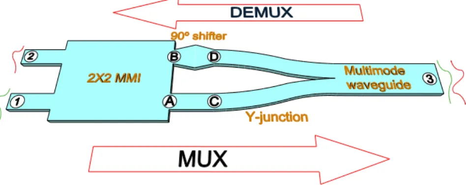
In this work we present for the first time a novel ultra-broadband two-mode converter and DE/MUX based on a sub-wavelength engineered MMI coupler, hereafter SWG-MMI, to overcome conventional MMIs constraints by means of dispersion engineering. Our device exhibits insertion losses below 0.84 dB and crosstalk lower than −20 dB in a 300 nm wavelength range (1.4−1.7 µm). The starting point of our proposed ultra-broadband mode converter and DE/MUX is the architecture based on a conventional MMI, shown in Fig. 1, which comprises, in addition to MMI, a 90◦ phase shifter and a Y-junction. At the design wavelegth of 1.55 µm, the input and output
ports of the device are two single mode access waveguides (ports 1 and 2) and one multimode access waveguide (port 3) as it can be seen in Fig. 1. When operating as a multiplexer (MUX), the fundamental mode in port 2 evolves to the first mode in port 3, and it is also combined with the fundamental mode coming from port 1. Conversely, when operating in reverse (DEMUX), the device demultiplexes the fundamental and the first mode from port 3 to ports 1 and 2, respectively.
In this case, the first mode in port 3 is also transformed into the fundamental mode in port 2. This paper is structured in four more sections. In section 2, the physical operation principle of the proposed device is explained. The design of each component of the ultra-broadband mode converter and DE/MUX is presented in section 3. Numerical simulation results of the whole device are discussed in section 4 and, finally, the main conclusions are summarized in section 5.
2. Principle of Operation
Mode DE/MUX based on a conventional MMI, a 90◦ phase shifter and a symmetric Y-junction
(see Fig. 1) are mainly restricted in bandwidth by the excess losses of the MMI [28], [29]. Conventional MMI couplers are based on the self-imaging principle [30], where the input field is reproduced in single or multiple images after propagating along a multimode waveguide of width WM M I. If we consider a 2x2 conventional MMI based on general interference, the length
of the multimode section is given by the following expression LM M I = 3Lπ/2, where Lπ is the
beat length between the first and the second order modes (TE0 and TE1) with effective indexes
n0 ef f andn 1 ef f respectively: Lπ(λ) = λ 2(n0 ef f(λ) − n 1 ef f(λ)) (1) Equation 1 shows that the beat length of conventional MMIs depends directly on the wavelength and, subsequently, self-images are formed at different lengths for every wavelength. Hence the intrinsic bandwidth limitation of conventional MMIs will also restrict the performance of conventional two-mode converter and DE/MUX, since the symmetric Y-junction has a broadband performance and it is verified that the conventional MMI limits the bandwidth performance more than the phase shifter. Nevertheless, an almost flat beat length can be achieved by means of engineering the dispersion of the guided modes in the multimode section of the MMI coupler, so that the index differencen0
ef f(λ) − n 1
ef f(λ) compensates the wavelength dependence and, in consequence, the
beat length remains almost constant with the wavelength [31], [32], [33]. For this reason, we propose to replace the conventional MMI with a SWG-MMI with a broader operation bandwidth. Accordingly, our proposed two-mode converter and DE/MUX is based on a SWG-MMI, a 90◦
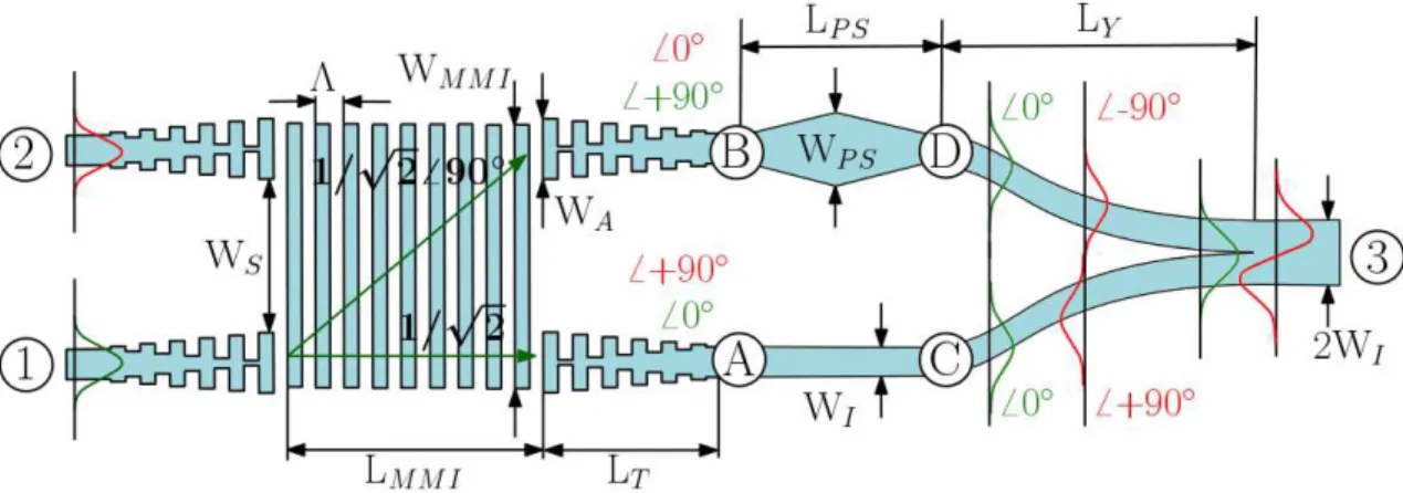
phase shifter (PS) and a symmetric Y-junction as shown in Fig. 2. The ultra-broadband behaviour of the SWG-MMI is achieved through dispersion engineering by means of sub-wavelength grating waveguides [31], [32]. SWG structures are formed by a disposition of different alternating materials that are repeated periodically with a pitch (Λ) smaller than the operating wavelength in order to avoid diffraction [33]. Thereby the 2x2 SWG-MMI works as its counterpart conventional 3 dB-90◦
hybrid coupler, i.e. a 90◦ phase shift is produced between the two output arms, but with a broader
operation bandwidth. The 90◦ PS is based on two parallel waveguides, where the upper arm
comprises two trapezoidal tapers in back-to-back configuration and the lower arm is a straight waveguide of width, WI, supporting only the fundamental mode. In this way, the effective index
of the mode propagated through the upper arm increases, i.e. it is delayed regarding the mode propagated through the lower arm, leading to a −90◦ phase shift for a certain PS length at the
wavelength of 1.55µm. In addition, the Y-junction stem of width 2WI supports both the first and
the second order modes.
The operation principle of the entire device is schematically shown in Fig. 2. If the device works as a MUX, the fundamental mode injected through port 1 (in green) is split by the SWG-MMI with the same amplitude and a phase difference of ∆ϕB − ϕA = +90◦ between the ports B
and A. The PS generates a −90◦ phase shift between the upper and lower arms, evolving the
total phase difference from +90◦ to 0 and resulting in two in-phase TE
0 modes. The symmetric
Y-junction combines these two modes in order to generate the TE0 output at the stem (port 3).
Moreover, when the fundamental mode is injected through port 2 (in red), it is also equally split by the SWG-MMI whereas the phase difference becomes∆ϕB− ϕA= −90◦. A total phase shift of
180◦is induced after the PS section, and the resulting two out-of-phase TE
Fig. 2. Schematic and principle of operation of the proposed two-mode converter and DE/MUX based on a SWG-MMI, a symmetric Y-junction and a 90◦phase shifter.
by means of the Y-junction to generate the TE1output. For the counter-propagating direction, i.e.
when the device is working as DEMUX, TE0and TE1modes are launched through the stem (port
3). The Y-junction splits the TE0 mode in two in-phase TE0 modes and after the PS section, the
TE0mode is coupled into port 1. Similarly, the TE1is split in two out-of-phase TE0modes by the
Y-junction and the TE0 mode is coupled into port 2.
3. Device Design
Silicon-on-insulator platform was considered for the design of the proposed two-mode converter and DE/MUX. Refractive indexes of silicon and silicon dioxide are, respectively, nSi= 3.476 and
nSiO2 = 1.444 at the central operation wavelength of λ = 1.55 µm. The high refractive index
contrast of SOI provides high modal confinement and leads to small device footprints. Material dispersion was taken into account in our full 3D simulations [34], [35] to design, verify and optimize each element of the two-mode converter and DE/MUX. Typical single-mode dimensions of 220-nm-thick and 500-nm-wide Si-wire waveguides surrounded by a SiO2 substrate and cladding
were chosen for the designed wavelength of 1.55µm. Single-mode condition is not met at shorter wavelengths of our simulation wavelength range (1.4−1.7 µm). However, residual higher-order modes at short wavelengths are weakly confined and can be filtered using a sharp bend without penalty for the fundamental mode. Hence, the width of the Y-junction stem is 2WI = 1 µm
supporting TE0 and TE1 modes.
Power transmission of the symmetric Y-junction depends on the angle between the two branches, and is lower for the fundamental mode injected through port 3 (green curve in Fig. 3) as the first mode injected at the same port (red curve in Fig. 3) has a null at the intersection. Since the excess losses are low, the performance of the Y-junction is almost the same when the fundamental mode is injected through port C or D. The separation of the branches has been set at 1.5µm. In order to achieve a compact device, the length of the Y-junction was reduced, i.e. a larger angle was chosen, until the losses began to increase excessively. Note that excess losses are also related with the bend radius of the arc type S-bends used for the branches and are determined by the separation and the angle. In this case, for a chosen angle ofθ/2 = 12◦and a separation of 1.5µm,
the bend radius is ∼17 µm, yielding a length of LY = 7.14 µm. In terms of bandwidth, symmetric
Y-junctions show a broad performance since their functionality only rely on geometrical design [36], although their main limitation is the fabrication of the junction between the two branches, typically resulting in a gap and introducing additional losses.
Physical design parameters of the SWG-MMI were taken from Halir et al. [32], who have recently demonstrated a novel SWG-MMI design with an ideal simulated performance over a 500 nm wavelength range, whereas the fabricated device exhibits a measured bandwidth over 300 nm.
(a) (b)
Fig. 3. S-parameters magnitude (a) and excess losses (b) as a function of the symmetric Y-junction angle, θ/2, when injecting the fundamental (green) and the first (red) modes through port 3. Inset: symmetric Y-junction scheme.
(a) (b)
Fig. 4. S-parameters magnitude (a) and phase difference between ports B and A (b) of the sub-wavelength engineered MMI (solid lines) compared to the conventional MMI (dotted lines) when injecting the fundamental mode through port 1. Ports definitions for the conventional MMI and the SWG-MMI are shown in Figs. 1 and 2, respectively.
The SWG structure presents a duty cycle (DC) of 50% in order to maximize the minimum feature size and a pitch (Λ) of 190 nm to achieve a maximally flat beat length of Lπ ≈ 10 µm, yielding
a three-fold reduction compared to a conventional MMI. The initial number of periods of the multimode section can be calculated asPM M I = (3Lπ/2)/Λ = 79 periods. An adiabatic transition
between conventional waveguides and periodic waveguides is performed by means of SWG tapers with a length ofLT = 5.7 µm, i.e. PT = 30 periods, adapting the effective index of the conventional
Si-wire waveguide to the effective index of the SWG region. Consequently, no higher-order modes are excited in the transition when only the fundamental mode is excited in the Si-wire waveguide. The access width of the SWG-MMI is WA= 1.7 µm and the separation between SWG tapers is
WS= 0.3 µm. Finally, optimization through iterative simulation of the SWG-MMI width and length
performed in [32] results in WM M I = 3.25 µm and LM M I = 14.06 µm, with PM M I = 74.
To be able to compare the performance of our proposed device, an equivalent two-mode converter and DE/MUX based on a conventional MMI is designed as well. Furthermore, the equivalent conventional MMI of Halir et al. [32] was chosen to maintain the consistency of the
(a) (b)
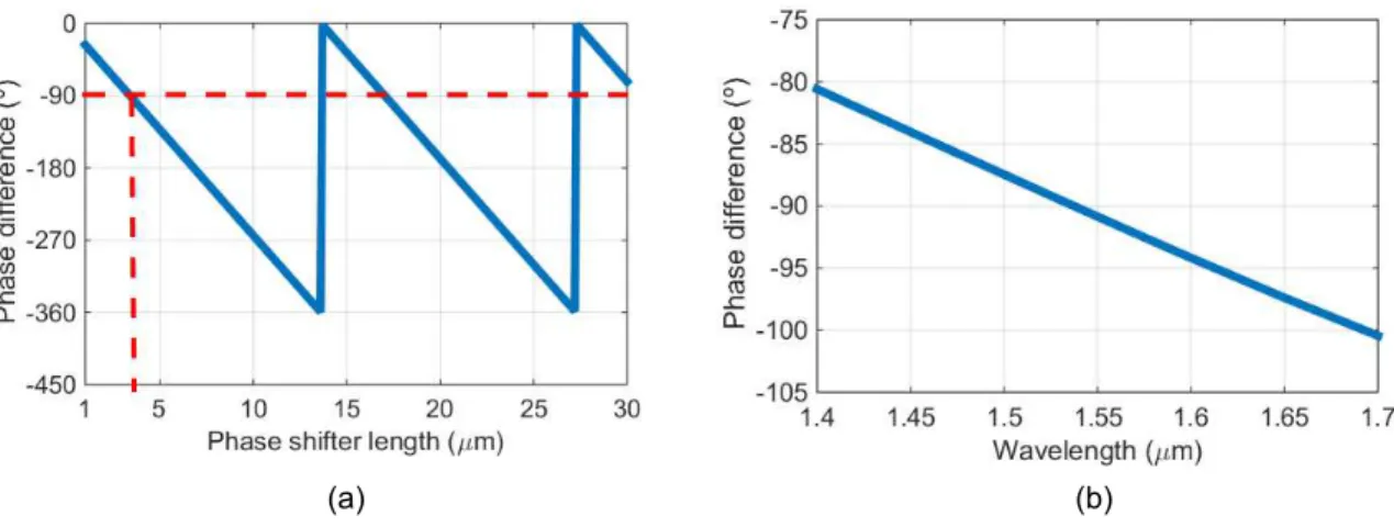
Fig. 5. Phase difference between the upper and lower arms as a function of the phase shifter length (a) and as a function of the wavelength for the selected length of LP S= 3.41 µm (b).
previous design. The conventional MMI has the same access width (WA), separation between
tapers (WS) and MMI width (WM M I) as the SWG-MMI. The length of the conventional MMI grows
up toLM M I = 38.5 µm and the length of the tapers is LT = 6 µm, yielding a total DE/MUX length
of 61 µm. Note that the same design will be kept for the symmetric Y-junction and for the PS. Figure 4 (a) shows the limitations imposed by the conventional MMI in terms of losses (lower values of the S-parameters magnitude) for the 300 nm wavelength range.
Regarding the PS design, Fig. 5 (a) shows the simulated phase difference between upper and lower arms as a function of the PS length. The width of the lower arm is WI = 0.5 µm, while
the widest part of the two trapezoids is set toWP S= 0.7 µm. A −90◦phase shift is achieved for
different PS lengths. As a compact DE/MUX is sought after the PS total length should beLP S=
3.41 µm to ensure a −90◦ phase shift and a broader bandwidth performance. In consequence,
the total length of the designed two-mode DE/MUX is as small as 36 µm when interconnection waveguides between the different elements are not considered. Deviations from the ideal 90◦
phase shift in the MMI and the PS result in a degradation of the performance (higher crosstalk values) of the DE/MUX. In this case, the conventional MMI also limits the crosstalk response compared to the PS due to the larger phase difference deviations (see Fig. 4 (b) and Fig. 5 (b)). It is necessary to emphasize that the MMI response is almost symmetric (see Fig. 4 (a)) and, in consequence, the Mach-Zehnder interferometer (MZI) is always balanced in power. Moreover, the PS and the Y-junction of the proposed device present low losses compared to the MMI. Assuming these conditions, it can be shown analytically that the performance of the device is very similar for MUX and DEMUX operation. The total losses are hence determined by the MMI losses, whereas the crosstalk is limited by the phase errors of the MMI and the phase shifter.
4. Simulation Results
Full 3D simulation [34], [35] of the complete device is not straightforward, due to the long simulation time. To leverage previous design simulations, S parameters matrices of the SWG-MMI, the PS and the symmetric Y-junction were separately calculated using 3D-FDTD, and subsequently, concatenated in order to obtain the S parameters of the complete device. Note that S parameters matrices were calculated as a correlation of the corresponding modes at each input/output port. It is also necessary to notice that the symmetric Y-junction works as a mode converter for the first and the second order modes, consequently, two simulations were required to obtain the S parameters for each mode.
(a) (b)
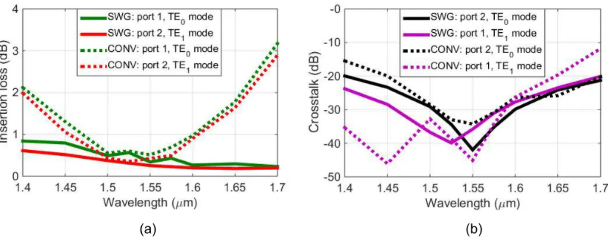
Fig. 6. Comparison of the insertion losses (a) and crosstalk (b) of our proposed device (solid curves) and the conventional equivalent device (dotted curves). Worst case has been taken into account, i.e. maximum of insertion losses and crosstalk for MUX and DEMUX configurations.
of our proposed ultra-broadband mode converter and DE/MUX. Two different definitions can be distinguished depending on whether the device is working as a MUX or as a DEMUX. For the MUX configuration, and for each input/output modal port, insertion losses are defined as the amount of power relative to the input power that is transferred to the desired mode, whereas the crosstalk is the power difference between the undesired and the desired modes. On the other hand, when the device operates as a DEMUX, insertion losses are the amount of power relative to the input power transferred to the desired output. Additionally, the crosstalk is the power difference between the undesired and the desired ports. Figure 6 (a) shows the maximum insertion losses as a function of the wavelength for the device working as MUX or DEMUX. When the TE0 mode
is launched through ports 1 and 2 (MUX), insertion losses are below 0.84 dB and 0.61 dB within the simulated wavelength range (1.4−1.7 µm), and almost the same values are obtained for the DEMUX configuration. Moreover, Fig. 6 (b) shows a crosstalk lower than −20 dB and −20.1 dB when the TE0 mode is launched through port 1 and 2 (MUX) for the undesired modes at the
outputs. Working as a DEMUX, the crosstalk is also below −20 dB and −20.1 dB for the TE0
and TE1modes respectively, within the same 300 nm wavelength range. The 25 nm displacement
between the two crosstalk curves atλ = 1.55 µm is caused by a small phase mismatch between the accumulated phase shift of the PS and the SWG-MMI. Return loss below −32.5 dB and −32 dB for TE0 and TE1 modes was estimated within the full bandwidth. In the wavelength range
from 1.5 µm to 1.6 µm, insertion losses decrease up to only 0.56 dB and 0.37 dB for the MUX configuration, and to 0.57 dB and 0.37 dB for the DEMUX configuration. The crosstalk, which is now mainly limited by the narrowband behaviour of the phase shifter, is also reduced to −29.1 dB and −27.7 dB for the MUX and DEMUX configurations. Figure 6 shows the maximum insertion losses and crosstalk, since differences between our proposed device operating as MUX and as DEMUX are almost negligible, proving the ultra-broadband performance of our proposed device for both configurations.
For the sake of comparison, Fig. 6 also shows the results of the equivalent DE/MUX based on a conventional MMI which were also obtained by 3D FDTD simulation of each individual component followed by S parameter concatenation. The conventional DE/MUX (dotted curves) exhibits insertion losses below 0.85 dB when the bandwidth is reduced to 100 nm (1.455−1.555 µm) and the crosstalk is similar for both DE/MUXs. Return loss is lower than −30.6 dB (TE0) and
−31.6 dB (TE1) in the same wavelength range. Therefore, a three-fold bandwidth enhancement is
achieved compared to the conventional design, besides a length reduction of 25.04µm. It should be noticed that the crosstalk for the TE1 mode is lower for the conventional MDM than for the
(a) (b) (c) 0.1 0.2 0.3 0.4 0.5 0.6 0.7 0.8 0.9 1
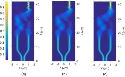
Fig. 7. Field distribution of the designed ultra-broadband DE/MUX when TE0mode is injected through
the multimode waveguide (port 3) at wavelengths 1.4 µm (a), 1.55 µm (b) and 1.7 µm (c).
(a) (b) (c) 0.1 0.2 0.3 0.4 0.5 0.6 0.7 0.8 0.9 1
Fig. 8. Field distribution of the designed ultra-broadband DE/MUX when TE1mode is injected through
the multimode waveguide (port 3) at wavelengths 1.4 µm (a), 1.55 µm (b) and 1.7 µm (c).
proposed SWG-MDM at the wavelength of 1.45µm, since the phase shift error of the conventional MMI and the PS are compensated (see Fig. 4 (b) and Fig. 5 (b)). The appearance of this effect is unusual and depends on the PS and the conventional MMI design.
The simulated field distribution of the designed ultra-broadband DE/MUX is shown in Fig. 7 and Fig. 8 atλ = 1.4 µm (a), λ = 1.55 µm (b) and λ = 1.7 µm (c) when the input field is the first order mode and the second order mode respectively. Figure 7 (a) and Fig. 8 (a) show some field ripples caused in part by the discontinuity of the symmetric Y-junction branches and by the presence of
(a) (b)
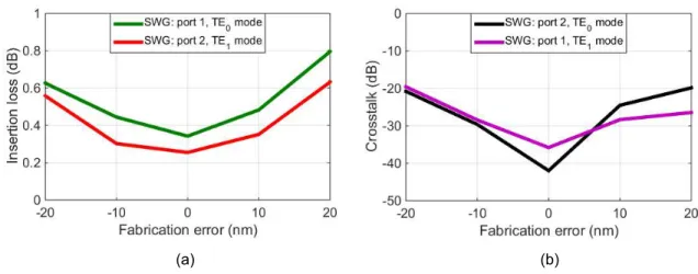
Fig. 9. Insertion losses (a) and crosstalk (b) for the worst case of the proposed ultra-broadband two-mode converter and DE/MUX as a function of fabrication error at λ=1.55 µm. Worst case has been taken into account, i.e. maximum of insertion losses and crosstalk for MUX and DEMUX configurations.
the TE1 mode at shorter wavelength. Y-junction contribution to ripples can be reduced with a
longer Y-junction, whereas TE1 mode can be readily filtered with a waveguide bend. Insertion
losses of the sub-wavelength engineered DE/MUX are higher at lower wavelengths due to the excess losses of the SWG-MMI and the Y-junction discontinuity, which presents a greater optical size at lower wavelengths.
In addition, width fabrication tolerances of each device were calculated independently in order to analyze the behaviour of the entire DE/MUX by means of S parameters matrices concatena-tion. We consider fabrication errors as absolute variations of the waveguide dimensions, e.g. a waveguide increases its width in +20 nm (10 nm per side) for a +20 nm error. To perform a trustworthy tolerance study regarding the SWG-MMI, the duty cycle was changed accordingly to the width changes. A critical parameter for the crosstalk of our proposed device is the fabrication error of the PS. For typical ±20 nm fabrication errors of the PS width, the phase shift error is under 11◦. Performance degradation of the SWG-MMI mostly depends on the duty cycle variation.
In our design, fabrication errors between ±20 nm of the duty cycle correspond to a ∼ ±10% pitch fractional error. Finally, Fig. 9 shows the maximum insertion losses (a) and crosstalk (b) as a function of fabrication error for our proposed ultra-broadband two-mode DE/MUX at the central operating wavelength of 1.55 µm. Fabrication errors between ±20 nm result in insertion losses under 0.8 dB and crosstalk below −19.5 dB.
5. Conclusions
In this work, an ultra-broadband two-mode converter and de/multiplexer comprised of a SWG-MMI, a 90◦ phase shifter and a symmetric Y-junction is proposed for the first time. We show
that the main restrictions are imposed by conventional MMIs used hitherto and we propose to replace it with a sub-wavelength engineered MMI. SWG structures enable dispersion engineering in order to suppress the limitations imposed by conventional MMIs, attaining a three-fold band-width enhancement with our proposed device compared to the equivalent DE/MUX based on a conventional MMI. Full 3D simulations of our proposed device in MUX and DEMUX configurations show insertion losses below 0.84 dB and 0.61 dB for TE0 and TE1 modes, respectively, within a
300 nm wavelength range (1.4−1.7 µm). The simulated crosstalk is lower than −20 dB for the TE0and TE1modes within the same wavelength range, and the overall footprint of the device is
as small as 36µm x 3.7 µm. Tolerance study shows good fabrication tolerances to errors between −20 nm and +20 nm for the entire device. Furthermore, the number of multiplexed modes can be
increased by scaling the MMI, while a lower crosstalk can be achieved by optimizing the phase shifter design. Finally, we believe that the results presented in this paper pave the way for compact mode-division multiplexing devices that can be used together with wavelength-division multiplexing to further increase bandwidth capacity in silicon photonic interconnects.
Acknowledgements
This work has been funded in part by the Spanish Ministry of Economy and Competitiveness under grants TEC2015-71127-C2-1-R (FPI scholarship BES-2016-077798), TEC2016-80718-R and FJCI-2014-22836; and the Community of Madrid (S2013/MIT-2790). This project has received funding from the EMPIR program (JRP-i22 14IND13 Photind), co-financed by the participating countries and the European Union’s Horizon 2020 research and innovation program; and from the Horizon 2020 research and innovation program under the Marie Sklodowska-Curie grant No. 734331.
References
[1] D. A. Miller, “Rationale and challenges for optical interconnects to electronic chips”, Proceedings of the IEEE, vol. 88, no. 6, pp. 728-749, June 2000.
[2] M. J. Paniccia, “A perfect marriage: optics and silicon”, Optik & Photonik, vol. 6, no. 2, pp. 34-38, May 2011. [3] D. A. Miller, “Device requirements for optical interconnects to silicon chips”, Proceedings of the IEEE, vol. 97, no. 7,
pp. 1166-1185, July 2009.
[4] A. Liu, L. Liao, Y. Chetrit, J. Basak, H. Nguyen, D. Rubin, and M. Paniccia, “Wavelength division multiplexing based photonic integrated circuits on silicon-on-insulator platform”, IEEE Journal of Selected Topics in Quantum Electronics, vol. 16, no. 1, pp. 23-32, Feb. 2010.
[5] S. Chen, Y. Shi, S. He, and D. Dai, “Compact monolithically-integrated hybrid (de) multiplexer based on silicon-on-insulator nanowires for PDM-WDM systems”, Optics Express, vol. 23, no. 10, pp. 12840-12849, May 2015. [6] B. Zhu, T. F. Taunay, M. Fishteyn, X. Liu, S. Chandrasekhar, M. F. Yan, J. M. Fini, E. M. Monberg, and F. V. Dimarcello,
“112-Tb/s space-division multiplexed DWDM transmission with 14-b/s/Hz aggregate spectral efficiency over a 76.8-km seven-core fiber”, Optics Express, vol. 19, no. 17, pp. 16665-16671, Aug. 2011.
[7] C. R. Doerr, and T. F. Taunay, “Silicon photonics core-, wavelength-, and polarization-diversity receiver”, IEEE Photonics Technology Letters, vol. 23, no. 9, pp. 597-599, May 2011.
[8] D. Dai, J. Wang, and S. He, “Silicon multimode photonic integrated devices for on-chip mode-division-multiplexed optical interconnects”, Progress In Electromagnetics Research, vol. 143, pp. 773-819, Nov. 2013.
[9] L. F. Frellsen, Y. Ding, O. Sigmund, and L. H. Frandsen, “Topology optimized mode multiplexing in silicon-on-insulator photonic wire waveguides”, Optics Express, vol. 24, no. 15, pp. 16866-16873, July 2016.
[10] L. Yang, T. Zhou, H. Jia, S. Yang, J. Ding, X. Fu, and L. Zhang, “General architectures for on-chip optical space and mode switching”, Optica, vol. 5, no. 2, pp. 180-187, Feb. 2018.
[11] J. Wang, S. Chen, and D. Dai, “Silicon hybrid demultiplexer with 64 channels for wavelength/mode-division multiplexed on-chip optical interconnects”, Optics Letters, vol. 39, no. 24, pp. 6993-6996, Dec. 2014.
[12] H. Xu, and Y. Shi, “Ultra-sharp multi-mode waveguide bending assisted with metamaterial-based mode converters”, Laser & Photonics Reviews, 1700240, Jan. 2018.
[13] L. H. Gabrielli, D. Liu, S. G. Johnson, and M. Lipson, “On-chip transformation optics for multimode waveguide bends”, Nature Communications, vol. 3, no. 1217, Nov. 2012.
[14] H. Xu, and Y. Shi, “Dual-mode waveguide crossing utilizing taper-assisted multimode-interference couplers”, Optics Letters, vol. 41, no. 22, pp. 5381-5384, Nov. 2016.
[15] C. Sun, Y. Yu, and X. Zhang, “Ultra-compact waveguide crossing for a mode-division multiplexing optical network”, Optics Letters, vol. 42, no. 23, pp. 4913-4916, Dec. 2017.
[16] J. Wang, S. He, and D. Dai, “On-chip silicon 8-channel hybrid (de) multiplexer enabling simultaneous mode- and polarization-division-multiplexing”, Laser & Photonics Reviews, vol. 8, no. 2, pp. L18-L22, Jan. 2014.
[17] B. A. Dorin, and N. Y. Winnie, “Two-mode division multiplexing in a silicon-on-insulator ring resonator”, Optics Express, vol. 22, no. 4, pp. 4547-4558, Jan. 2014.
[18] Z. Zhang, Y. Yu, and S. Fu, “Broadband on-chip mode-division multiplexer based on adiabatic couplers and symmetric Y-junction”, IEEE Photonics Journal, vol. 9, no. 2, pp. 1-6, Apr. 2017.
[19] J. Wang, Y. Xuan, M. Qi, H. Huang, Y. Li, M. Li, X. Chen, Z. Sheng, A. Wu, W. Li, X. Wang, S. Zou and F. Gan, “Broadband and fabrication-tolerant on-chip scalable mode-division multiplexing based on mode-evolution counter-tapered couplers”, Optics Letters, vol. 40, no. 9, pp. 1956-1959, May 2015.
[20] J. B. Driscoll, R. R. Grote, B. Souhan, J. I. Dadap, M. Lu, and R. M. Osgood, “Asymmetric Y junctions in silicon waveguides for on-chip mode-division multiplexing”, Optics Letters, vol. 38, no. 11, pp. 1854-1856, June 2013. [21] H. C. Chung, K. S. Lee, and S. Y. Tseng, “Short and broadband silicon asymmetric Y-junction two-mode (de)
multiplexer using fast quasiadiabatic dynamics”, Optics Express, vol. 25, no. 12, pp. 13626-13634, June 2017. [22] L. Han, S. Liang, H. Zhu, L. Qiao, J. Xu, and W. Wang, “Two-mode de/multiplexer based on multimode interference
[23] P. Cheben, DX. Xu, S. Janz, and A. Densmore, “Subwavelength waveguide grating for mode conversion and light coupling in integrated optics”, Optics Express, vol. 14, no. 11, pp. 4695-4702, May 2006.
[24] P. Cheben, P. J. Bock, J. H. Schmid, J. Lapointe, S. Janz, DX. Xu, A. Densmore, A. Del ˆage, B. Lamontagne, and T. J. Hall, “Refractive index engineering with subwavelength gratings for efficient microphotonic couplers and planar waveguide multiplexers”, Optics Letters, vol. 35, no. 15, pp. 2526-2528, July 2010.
[25] D. P ´erez-Galacho, D. Marris-Morini, A. Ortega-Mo ˜nux, J. G. Wang ¨uemert-P ´erez, and L. Vivien, “Add/drop mode-division multiplexer based on a machzehnder interferometer and periodic waveguides”, IEEE Photonics Journal, vol. 7, no. 4, pp. 1-7, July 2015.
[26] Z. Jafari, A. Zarifkar, and M. Miri, “Compact fabrication-tolerant subwavelength-grating-based two-mode division (de) multiplexer”, Applied Optics, vol. 56, no. 26, pp. 7311-7319, Sep. 2017.
[27] W. Chang, M. Zhang, L. Lu, F. Zhou, D. Li, Z. Pan, and D. Liu, “Inverse design of an ultra-compact mode (de) multiplexer based on subwavelength structure”, in CLEO: Science and Innovations. Optical Society of America, pp. SF1J-8, May 2017.
[28] Y. Li, C. Li, C. Li, B. Cheng, and C. Xue, “Compact two-mode (de) multiplexer based on symmetric Y-junction and multimode interference waveguides”, Optics Express, vol. 22, no. 5, pp. 5781-5786, Mar. 2014.
[29] F. Guo, D. Lu, R. Zhang, H. Wang, and C. Ji, “A two-mode (de) multiplexer based on multimode interferometer coupler and y-junction on InP substrate”, IEEE Photonics Journal, vol. 8, no. 1, pp. 1-8, Feb. 2016.
[30] L. B. Soldano, and E. C. Pennings, “Optical multi-mode interference devices based on self-imaging: principles and applications”, Journal of Lightwave Technology, vol. 13, no. 4, pp. 615-627, Apr. 1995.
[31] A. Maese-Novo, R. Halir, S. Romero-Garc´ıa, D. P ´erez-Galacho, L. Zavargo-Peche, A. Ortega-Mo ˜nux, I. Molina-Fern ´andez, J. G. Wang ¨uemert-P ´erez, and P. Cheben, “Wavelength independent multimode interference coupler”, Optics Express, vol. 21, no. 6, pp. 7033-7040, Oct. 2013.
[32] R. Halir, P. Cheben, J. M. Luque-Gonz ´alez, J. D. Sarmiento-Merenguel, J. H. Schmid, J. G. Wang ¨uemert-P ´erez, DX. Xu, S. Wang, A. Ortega-Mo ˜nux, and I. Molina-Fern ´andez, “Ultra-broadband nanophotonic beamsplitter using an anisotropic sub-wavelength metamaterial”, Laser & Photonics Reviews, vol. 10, no. 6, pp. 1039-1046, Nov. 2016. [33] R. Halir, P. J. Bock, P. Cheben, A. Ortega-Mo ˜nux, C. Alonso-Ramos, J. H. Schmid, J. Lapointe, DX. Xu,
J. G. Wang ¨uemert-P ´erez, I. Molina-Fern ´andez, and S. Janz, “Waveguide sub-wavelength structures: a review of principles and applications”, Laser & Photonics Reviews, vol. 9, no. 1, pp. 25-49, Sep. 2015.
[34] “FullWAVE, available from RSoft, https://optics.synopsys.com/rsoft/”. [35] “FemSIM, available from RSoft, https://optics.synopsys.com/rsoft/”.
[36] J. D. Love, and N. Riesen, “Single-, few-, and multimode Y-junctions”, Journal of Lightwave Technology, vol. 30, no. 3, pp. 304-309, Feb. 2012.