HAL Id: hal-00222942
https://hal.archives-ouvertes.fr/hal-00222942
Submitted on 30 Jan 2008
HAL is a multi-disciplinary open access
archive for the deposit and dissemination of sci-entific research documents, whether they are pub-lished or not. The documents may come from teaching and research institutions in France or abroad, or from public or private research centers.
L’archive ouverte pluridisciplinaire HAL, est destinée au dépôt et à la diffusion de documents scientifiques de niveau recherche, publiés ou non, émanant des établissements d’enseignement et de recherche français ou étrangers, des laboratoires publics ou privés.
Polarization insensitive blazed diffraction gratings
Nicolas Bonod, E. Popov, Stefan Enoch, Jérôme Neauport
To cite this version:
Nicolas Bonod, E. Popov, Stefan Enoch, Jérôme Neauport. Polarization insensitive blazed diffraction gratings. Journal of the European Optical Society : Rapid publications, European Optical Society, 2006, 1 (1), pp.06029-1-8. �hal-00222942�
Polarization insensitive blazed diffraction gratings
Nicolas Bonod1, Evgeny Popov1, Stefan Enoch1, Jérôme Néauport2
1
Institut Fresnel, Université de Provence, CNRS UMR 6133, 13397 Marseille Cedex 2
Commissariat à l’Energie Atomique, Centre d’études scientifiques et techniques d’Aquitaine, BP2, 33114 Le Barp
Abstract: Gratings insensitive to light polarization may be useful in many areas of optical
engineering, particularly in light demultiplexing application. We study different kinds of binary gratings able to present reflected efficiencies higher than 98% in the –1st order. These are metallic gratings, dielectric gratings deposited on a metallic substrate, total internal reflection gratings and gratings lying on a dielectric multilayer. We study each configuration with respect to manufacturing constraints and optical performances to conclude by providing the most suitable design.
1. Introduction
Gratings present dispersive properties which are widely used in spectroscopy analysis, light demultiplexing and also in ultrashort pulse compression1. In many cases, they are used to disperse unpolarized incident light. Unfortunately, their diffractive properties are largely dependent on light polarization, therefore inducing undesired polarization dependent losses, undesirable for applications such as light demultiplexing2. This paper is devoted to the design of gratings able to diffract almost 100% of the incident light in a specific dispersive -1st order simultaneously for both transverse magnetic (TM) and electric (TE) polarization.
Three steps are necessary to diffract all the incident light in the -1st order in reflection.
• The first one is to reflect the incident light. Metallic substrates, dielectric substrate used in total internal reflection, multilayer dielectric layers or photonic crystals can be used for this purpose.
• The second step is to etch a grating in the reflecting device. The ratio between the period and the incident wavelength determines the number of propagative orders. As the incident light energy is desired to be almost entirely diffracted into one specific order, the number of propagating orders must be minimal. When the angle of incidence is known, the number of propagating orders is only determined by the ratio between the wavelength λ and the grating period d. The specular (0) order is always propagative and does not present dispersive properties. The second propagating order is usually the -1st order. As a consequence, the grating period is determined to induce only two propagative orders. The exception to this rule concernes echelles, grating with large period that blaze into an order with large number. They can be characterized with high values of efficiency in unpolarized light, however, the free spectral range in each diffraction order is quite limited.
• Finally, the last step consists of optimizing grating grooves profile to disperse all the incident light into the –1st order.
In this paper, we will study different kinds of binary gratings which can diffract as much as possible the incident light in the –1st order at the Littrow incidence. In the first section, we will consider two different metallic gratings. In the first case, the modulated layer lies in the metallic material, and in the second case, in a silica layer deposited onto the metallic substrate. In the second section, dielectric gratings based on total internal reflection phenomenon will be studied. These gratings are well known to diffract with a very good efficiency the incident light in the -1st order but to the best of our knowledge, no design has been proposed to make them insensitive to the incident polarization3,4. The third section is devoted to gratings etched on the surface of dielectric reflecting multilayers. We shall study both gratings recorded either on a dielectric mirror (HL)7HL made of SiO2 (for L) and HfO2 (for H) or on a 2 dimensional photonic crystal made of macroporous silicon.
The wavelength is equal to 1.55 µm for telecommunication applications and the period d is 1.33 µm, except in the second section where the total internal reflection condition imposes a lower period taken equal to 0.6 µm. The Littrow incidence in air is defined by sinθ-1=λ/(2d), where θ-1 is the angle of refraction of the –1st order, and is equal to 35.5 deg1. It is well known that this incidence favourites the diffraction in the -1st order1.
Optimizations are made using a numerical code based on the differential method5. This method enables the rigorous resolution (to the numerical approximations) of Maxwell equations in periodic media.
2. Gratings based on metallic reflector
2.1. Metallic modulated area
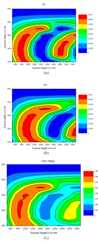
The most common metallic grating is a grating presenting a periodical modulation of the metallic surface. In practice, the relief is recorded in a photosensitive resin deposited onto a dielectric substrate (glass). After the photosensitive resin development, the modulated surface is coated by a metallic layer. The modulation can also be transferred directly into the dielectric substrate by ion etching technique and then coated by a metallic layer. In all these cases, the metallic layer is thick enough to be considered as the substrate and the device can be represented schematically as in fig.1. The efficiency in the -1-st reflected order are calculated in TE and TM polarization as a function of the groove height h and width c, and the calculated efficiencies are given in fig.2 in TE (fig.2a) and TM (fig.2b) polarization together with their mean values(fig.2c). As it can be observed, the reflected efficiency in the -1st order depends highly on the polarization, and we can see in fig.2c that the unpolarized efficiency does not reach 95%. The use of the metal introduces too much losses thus limiting the efficiency to approximately 90% in both TE and TM polarization.
2.2. Dielectric modulated area
Let us now consider gratings made of a modulated dielectric layer deposited on a flat metallic substrate. The modulation is made into a usual dielectric material like silica deposited on a metallic reflective substrate. Silica presents a low refractive optical index allowing a larger tolerance to manufacturing imprecision with respect to the original profile. Gold is chosen since, compared to silver, it presents a much lower reflectivity at a wavelength λ/3, used during the interference recording of the grating, which fact is of great importance in reducing the
standing-wave effect inside the photoresist. The device under study is depicted in fig.3. It has been shown recently that such grating can diffract 99% of the incident light into the -1st order6 in TE polarization. Guided modes in the silica layer are radiated by the modulated structure and constructive interferences between the propagated modes explain the almost perfectly diffraction6.
The efficiency calculated as a function of the two parameters h, c with e = 50 nm is shown in figs.4. The mean value of diffraction efficiencies in both polarizations is higher than 95%. However, manufacturing of such profiles will be a hard task due to the large value of the groove height compared to the wavelength. Moreover, the groove width values, around 0.4 µm, which lead to the highest reflected efficiencies are small compared to the period d (c/d = 0.3, and h/λ > 1). And indeed, conventional technologies used by grating manufacturers allow ratios c/d around 0.3 only when the ratio h/λ is largely smaller than 1. Despite this technological limitation, such a grating present attractive properties.
3. Total internal reflection gratings
In order to avoid the use of metal, undesirable for high energy applications, dielectric gratings based on the total internal reflection condition are now considered. The modulated area is illuminated from the material having higher optical index n. It is now well known that this kind of grating can diffract almost all of the incident light in the -1st order3,4. We first define the conditions on the grating period in order to satisfy the total internal reflection condition with two orders of propagations in Littrow incidence θi. The total internal condition writes :
sinθi > 1/n The Littrow incidence is defined by:
sinθ-1= −λ/(2nd) With the use of the two preceding conditions, one obtains:
d < λ/2
The -1st order is propagating if:
d > λ/2n
Finally, the condition imposed on the grating period writes:
λ/2n < d < λ/2
With λ = 1550 nm and n = 1.45, one obtains:
534 nm< d <775 nm
The period is taken equal to d = 600 nm and the Littrow incidence is then equal to sinθI = λ/2nd = 63°. Calculations of efficiencies, similar to the preceding section as a function of d and c lead to results shown in figs.6. The average between diffraction efficiencies in TE and TM polarization reaches 98%, unfortunately on a very narrow area. The optical properties of this grating appear to be highly dependent on the groove geometry, which is a severe technological limitation.
4. Multilayer dielectric gratings
The most common dielectric reflecting device is the well known dielectric Bragg mirror. A stack of alternatively high and low optical index material is deposited onto a dielectric substrate. The optical thickness of the layers is equal to λ/4nicosθi where ni is the optical index of the I-th layer and θi is the angle of refraction of the plane wave in this layer. The stack under study contains 7 bilayers of high and low optical index plus a layer of high optical index on the top, and is denoted as (HL)7H. A thicker layer of low-index material is then deposited to be etched periodically. The residual thickness of the low-index is denoted as e (fig.7). This kind of grating
was designed in the middle of the 90’s to increase the laser damage threshold of gratings used for ultrashort laser pulses compression7-8.
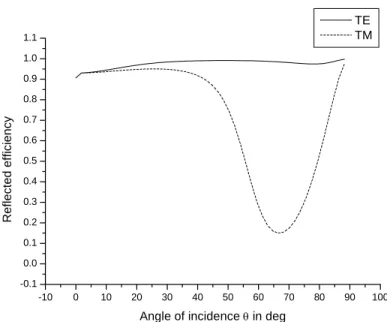
At first, we study the reflectivity of the mirror (HL)7H as a function of the angle of incidence θ for the both polarizations (fig.8). As the reflectivity is much better in TE polarization than in TM polarization, we expect to observe diffracted efficiencies largely dependent on the polarization. And indeed, the averaged reflectivity does not reach 90%, due to the insufficient reflectivity of the stack (fig.9) in TM polarization. To eliminate this difficulty, we can increase the number of bilayers, but mechanical stress grows resulting in crackings inside the stack or deformation of the wavefront depending on the coating process.
Another possibility is to increase the optical contrast between the layers. Let us increase the value of the high optical index up to 3.4, which corresponds to the silicon at λ=1.55 µm, keeping the same number of bilayers. We can observe in fig.10 that the increase of the optical contrast leads to a better reflectivity of the dielectric mirror, even if the reflectivity in TM polarization is still lower, especially at grazing incidences.
The same calculations of efficiency as a function of h and c result in plots shown in fig. 11. It is well shown in fig.11c that diffraction efficiency in the -1st order in unpolarized light is higher than 97% over a large area, i.e. with high tolerances to manufacturing defaults. As a consequence, a grating based on a high-contrast dielectric mirrors appears to be well adapted for the design of polarization insensitive gratings.
5. Photonic crystal diffraction grating
Nowadays, the progress of technology has made possible the realization of 2D photonic crystals. They appear as new opportunities to design reflection gratings. We have chosen a photonic crystal consisting of square holes in a silicon matrix9. The geometry is invariant in the z
direction, periodic and infinite in the x direction (fig.12). The period d of square holes (0.66 µm) equal to the half of the grating period (1.33 µm), is small enough to prevent propagation of dispersive orders. In the y direction, photonic crystal is made of 8 layers of periodical square holes of length equal to 0.8d. Substrate is pyrex, and cladding is air. The residual thickness of silicon above and below the square lattice is equal to the half of the thickness of the layer positioned between the two layers of periodic square holes, i.e, equal to d(sin(π/3)-0.8)/2. This photonic crystal presents photonic band gaps common to both TE and TM polarizations, centred around the wavelength of study 1.55 µm. The reflectivity of the device is studied as a function of the angle of incidence at λ=1.55 µm for both polarizations (fig.13). It can be observed that the reflectivity is almost perfect for both polarizations over a broad range of incidence. Contrary to the dielectric mirror studied in the preceding section, the reflectivity of the photonic crystal is better in TM polarization than in TE polarization.
To observe the propagation of the -1st dispersive order, a grating with period 2d is etched in a silica layer deposited on the top of the photonic crystal, with a residual thickness of silica denoted e (Fig.13). Such a device can be called photonic crystal diffraction grating11. To rigorously model such a device, a numerical code has been developed to solve Maxwell equations in periodical devices presenting 2 periods, one being twice bigger than the other.
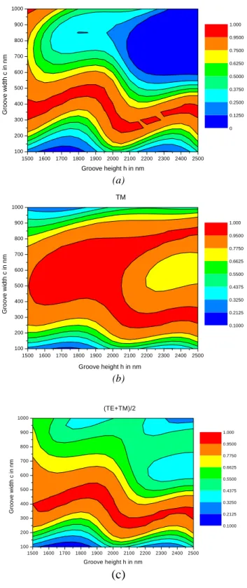
Calculations of efficiencies as a function of groove width c and height h similar to preceding sections is undertaken. Mean efficiency higher than 97% can be observed over a large area of ggrrov parameters (fig.14). Moreover, the groove width values leading to the highest reflected efficiencies are increased compared to the study of metallic grating (fig.4c), which makes easier the manufacturing of the profile.
To conclude this study, the angular tolerances of both the grating and the photonic crystal are compared. The reflected efficiencies are calculated as a function of the incident angle θ with profile dimensions h = 1850 nm and c = 450 nm, a couple which leads to the highest mean efficiency. We present in figs.15 the -1st order and the sum of the both reflected orders (0th and –1st) as a function of θ, for both TE (15.a) and TM (15.b) polarizations. The sum of the reflected efficiencies is directly related to the angular tolerance of the photonic crystal, and as expected, we can observe in fig.15 the perfect reflection of the device over the range of incidence and conclude that the angular tolerance of the photonic crystal diffraction grating is imposed by the angular tolerance of the grating.
Conclusion
We discuss different possibilities to design binary diffraction gratings able to diffract almost all the incident light (98%) in the –1st order in reflection, simultaneously for both fundamental polarizations. These gratings may considerably reduce the polarization dependent losses in telecommunication applications. We have studied and compared several types of gratings based on: metallic mirror, total internal reflection phenomenon and photonic crystal band gaps. Diffraction efficiencies of gratings with a metallic modulated surface are limited by losses induced by the metal, despite of the use of a highly conducting metal (silver). Much better performances are obtained when the modulated area lies inside a dielectric layer made of silica, whatever the reflecting device. Mean efficiencies averaged on both polarizations can reach values as high as 98% . The criterion used to select the best design is the stability of optical properties with respect to variations of groove geometry induced by technological processes. Large optical tolerance are obtained in figs.(4,6,13), in which the domain of high reflected efficiencies (> 95%) covers a large area of groove parameters . The largest area is obtained in
case of diffraction grating recorder on a 2D photonic crystal. This device appears to have high tolerances with respect to groove profile variations and provides polarization insensitive properties around values of c slightly lower than d/2 and h slightly higher than λ, which are easily accessible with actual technology. Photonic crystals are able to reflect light over a large range of angle of incidence. In order to know if this property may be useful for the design of grating poorly sensitive to incidence, reflected efficiencies of both propagating orders are plotted as a function of the angle of incidence. It is clearly shown that the angular tolerance is only determined by the grating's one since the sum of the both orders is almost equal to 1 over the whole range of incidence.
References
1. G. Loewen and E. Popov, Diffraction Gratings and Applications (Marcel Dekker, Inc, 1997) 2. E. Popov, J. Hoose, B. Frankel, C. Keast, M. Fritze, T. Y. Fan, D. Yost, and S. Rabe, "Low polarization dependent diffraction grating for wavelength demultiplexing," Opt. Express 12, 269-275 (2004)
3. E. Popov, L. Mashev, and D. Maystre, "Back-side diffraction by relief gratings," Opt. Commun. 65, 97-100 (1988)
4. J. R. Marciante and D. H. Raguin, "High efficiency, high dispersion diffraction gratings based on total internal reflection," Opt. Lett. 29, 542-544 (2004)
5. M. Nevière, E. Popov, Light propagation in periodic medias ; differential theory and design, (Marcel Dekker, New York, Basel, Honk Kong, 2003)
6. N. Destouches, A. Tishchenko, J. Pommier, S. Reynaud, O. Parriaux, S. Tonchev, M. Ahmed, "99% efficiency measured in the –1st order of a resonant grating," Opt. Express 13, 3230-3235 (2005)
7. M. D. Perry, R. D. Boyd, J. A. Britten, B. W. Shore, C. Shannon and L. Li, "High efficiency multilayer dielectric diffraction gratings", Opt. Lett. 20, 940-942 (1995)
8. N. Bonod, J. Néauport, "Optical performances and laser induced damage threshold improvement of diffraction gratings used as compressor in ultra high intensity laser," Opt. Commun. 260, 649-655 (2006)
9. K. Sakoda, Optical Properties of Photonic Crystals, (Springer, Berlin, 2001)
10. E. Popov, B. Bozhkov, and M. Neviere, "Almost perfect blazing by photonic crystal rods gratings," Apll. Opt. 40, 2417-2422 (2001)
12. D. Strickland and G. Mourou, "Compression of amplified chirped optical pulses," Opt. Commun. 56, 219-221 (1985)
13. A. J. Waddie, M. J. Thomson, and M. R. Taghizadeh, "Comparison of one- and
two-dimensional dielectric reflector geometries for high-energy laser pulse compression," Opt. Lett.
List of figures
Fig.1. Binary grating with groove height h and width c. The grating is illuminated by a monochromatic plane wave of wavelength λ = 1.55 µm, with angle of incidence θ. Grating period d is equal to 1.33 µm. Substrate is made of silver of optical index n = 0.322+ i10.9935 and cladding is air.
Fig.2 . Efficiencies in the -1st reflected order as a function of groove width c and height h. (a): TE polarization, (b) TM polarization, (c) mean values of efficiencies for TE and TM polarization.
Fig.3. A silica layer is deposited on a metallic substrate (gold) and etched periodically with a period d, a groove thickness h and width c. The residual thickness of silica is e.
Fig.4. Same as fig.2, but for the grating presented in fig.3.
Fig.5. Binary grating, working in total internal reflection and etched in silica illuminated by a monochromatic plane wave from the cladding made of silica, substrate is air.
Fig.6.Same as figs.2 and 4, but for the grating presented in fig.5
Fig.7. Multilayer dielectric grating (HL)7H. Substrate is pyrex, high optical index material is HfO2, and low optical index material is SiO2.
Fig.8 . Reflectivity of the dielectric mirror (HL)7H. nH = 1.9 and nB = 1.46.
Fig.9. Efficiency of the -1st order in reflection, averaged in TE and TM polarizations with e = 50 nm.
Fig.10. Reflectivity of the dielectric mirror (HL)7H. nH = 3.4 and nL = 1.46.
Figs.11.Efficiency in the -1st reflected order averaged between the both polarizations of the grating recorded on the stack (HL)7HL with nH = 3.4 and nL = 1.46, e = 50 nm.
Figs.12.(a) A 2 dimensional photonic crystal of triangular lattice, finite in the y direction, infinite and periodic in the x direction, and invariant in the z direction. It is made of 8 periodically modulated layers of period d = 0.66 µm. Square holes made in silicon have a length equal to 0.8d. (b) A grating is etched in a silica layer deposited on the photonic crystal. The grating period is twice bigger than the square holes period d.
Fig.13. Average of diffraction efficiencies in TE and TM polarization as a function of groove height and width for the grating made inside a silica layer deposited on the top the photonic crystal at Littrow incidence with λ=1.55µm.
Fig.14. The 0th (line) and -1st (dashed line) reflected orders and their sum (dotted line) of the photonic crystal diffraction grating as a function of the angle of incidence θ, with h = 1850 nm and c = 450 nm. TE (a) and (TM) (b) polarization.
Figure 1
Ag
Air, n=1
h
c
θ
d
N. Bonod et al.Figure 2 600 800 1000 1200 1400 1600 1800 2000 200 400 600 800 1000 TE 0 0.1250 0.2500 0.3750 0.5000 0.6250 0.7500 0.9500 1.000 Groove height h in nm G roove w id th c in n m 600 800 1000 1200 1400 1600 1800 2000 200 400 600 800 1000 TM 0 0.1250 0.2500 0.3750 0.5000 0.6250 0.7500 0.9500 1.000 Groove height h in nm Gr o o v e w idt h c in n m 600 800 1000 1200 1400 1600 1800 2000 200 400 600 800 1000 (TE+TM)/2 0 0.1250 0.2500 0.3750 0.5000 0.6250 0.7500 0.9500 1.000 Groove height h in nm Groo v e w idth c i n nm N. Bonod et al.
Figure 3 θi SiO2, n=1.45 Au Air, n=1 e h c d N. Bonod et al.
Figure 4 1500 1600 1700 1800 1900 2000 2100 2200 2300 2400 2500 100 200 300 400 500 600 700 800 900 1000 0 0.1250 0.2500 0.3750 0.5000 0.6250 0.7500 0.9500 1.000 Groove height h in nm G roove w idt h c i n nm (a) 1500 1600 1700 1800 1900 2000 2100 2200 2300 2400 2500 100 200 300 400 500 600 700 800 900 1000 TM Gro o ve w idth c in n m Groove height h in nm 0.1000 0.2125 0.3250 0.4375 0.5500 0.6625 0.7750 0.9500 1.000 (b) 1500 1600 1700 1800 1900 2000 2100 2200 2300 2400 2500 100 200 300 400 500 600 700 800 900 1000 (TE+TM)/2 0.1000 0.2125 0.3250 0.4375 0.5500 0.6625 0.7750 0.9500 1.000 Groove height h in nm G roo v e width c i n nm (c) N. Bonod et al.
Figure 5 θi θ0 θ-1 air silica, n=1,45 c h N. Bonod et al.
Figure 6 600 800 1000 1200 1400 1600 1800 2000 2200 2400 100 200 300 400 500 TE 0 0.1250 0.2500 0.3750 0.5000 0.6250 0.7500 0.9500 1.000 Groove height h in nm Gr oov e w idth c i n nm (a) 600 800 1000 1200 1400 1600 1800 2000 2200 2400 100 200 300 400 500 TM 0 0.1250 0.2500 0.3750 0.5000 0.6250 0.7500 0.9500 1.000 Groove height h in nm G roov e w idt h c i n nm (b) 600 800 1000 1200 1400 1600 1800 2000 2200 2400 100 200 300 400 500 (TE+TM)/2 0 0.1250 0.2500 0.3750 0.5000 0.6250 0.7500 0.9500 1.000 Groove height h in nm G roov e w idt h c in nm (c) N. Bonod et al.
Figure 7 S u b strate tH tL tH nH nL nH L o w o p tic al in d ex H igh o p tical in d ex nL h e θ c N. Bonod et al.
Figure 8 -10 0 10 20 30 40 50 60 70 80 90 100 -0.1 0.0 0.1 0.2 0.3 0.4 0.5 0.6 0.7 0.8 0.9 1.0 1.1 Refl ected effi ci ency
Angle of incidence θ in deg
TE TM
Figure 9 600 800 1000 1200 1400 1600 1800 2000 2200 2400 100 200 300 400 500 600 700 800 900 1000 TE polarization 0 0.1250 0.2500 0.3750 0.5000 0.6250 0.7500 0.9500 1.000 Groove height h in nm Gr o o ve w idt h c i n nm 600 800 1000 1200 1400 1600 1800 2000 2200 2400 100 200 300 400 500 600 700 800 900 1000 TM polarization 0 0.1250 0.2500 0.3750 0.5000 0.6250 0.7500 0.9500 1.000 Groove height h in nm Gro o ve w idth c in nm 600 800 1000 1200 1400 1600 1800 2000 2200 2400 100 200 300 400 500 600 700 800 900 1000 (TE+TM)/2 0 0.1250 0.2500 0.3750 0.5000 0.6250 0.7500 0.9500 1.000 Groove height h in nm G roo v e wi dt h c i n n m N. Bonod et al.
Fig.10 -10 0 10 20 30 40 50 60 70 80 90 100 0.0 0.1 0.2 0.3 0.4 0.5 0.6 0.7 0.8 0.9 1.0 1.1 1.2 Refl ected effi ci ency
Angle of incidence θ in deg
TE TM
Fig.11. 600 800 1000 1200 1400 1600 1800 2000 2200 2400 100 200 300 400 500 600 700 800 900 1000 TE polarization 0 0.1250 0.2500 0.3750 0.5000 0.6250 0.7500 0.9500 1.000 Groove height h in nm Gro o ve w idth c i n nm (a) 600 800 1000 1200 1400 1600 1800 2000 2200 2400 100 200 300 400 500 600 700 800 900 1000 TM polarization 0 0.1250 0.2500 0.3750 0.5000 0.6250 0.7500 0.9500 1.000 Groove hieght h in nm Gr oov e w idth c in nm (b) 600 800 1000 1200 1400 1600 1800 2000 2200 2400 100 200 300 400 500 600 700 800 900 1000 (TE+TM)/2 0 0.1250 0.2500 0.3750 0.5000 0.6250 0.7500 0.9500 1.000 Groove height h in nm G roov e w idt h c i n n m (c) N. Bonod et al.
Figure 12 n=1.45 z x y h n=1.45 n=1 θ c d (a)
h
n=1.45
n=1
θ
c
n=3.4
n=1.
(b) N. Bonod et al.Figure 13 1500 1600 1700 1800 1900 2000 2100 2200 2300 2400 2500 100 200 300 400 500 600 700 800 900 1000 TE polarization 0 0.1250 0.2500 0.3750 0.5000 0.6250 0.7500 0.9500 1.000 Groove height h in nm Groove w idt h c i n nm (a) 1500 1600 1700 1800 1900 2000 2100 2200 2300 2400 2500 100 200 300 400 500 600 700 800 900 1000 TM polarization 0.1000 0.2125 0.3250 0.4375 0.5500 0.6625 0.7750 0.8875 1.000 Groove height h in nm Groov e w idt h c in nm (b) 1500 1600 1700 1800 1900 2000 2100 2200 2300 2400 2500 100 200 300 400 500 600 700 800 900 1000 (TE+TM)/2 0.1000 0.2125 0.3250 0.4375 0.5500 0.6625 0.7750 0.9500 1.000 Groove height h in nm G roo ve w idt h c in nm (c) N. Bonod et al.
Figure 14 -10 0 10 20 30 40 50 60 70 80 90 100 0.0 0.2 0.4 0.6 0.8 1.0 TE polarization re fle c te d e fficien cy
Angle of incidence θ in deg
(0) (-1) sum (a) -10 0 10 20 30 40 50 60 70 80 90 100 0.0 0.2 0.4 0.6 0.8 1.0 TM polarization re fl ected effi ci e n c y
Angle of incidence θ in deg
(0) (-1) sum
(b)