Custom Power Supply Interface for Teaching
MAWv"
C ircu it D esig n
H S-T, A M~ rEby
JUL
15 2014
Ruben E. Madrigal
IB
R
.LIBRAR[ES
Submitted to the Department of Electrical Engineering and Computer
Science
in partial fulfillment of the requirements for the degree of
Master of Engineering in Electrical Engineering and Computer Science
at the
MASSACHUSETTS INSTITUTE OF TECHNOLOGY
February 2014
@
Massachusetts Institute of Technology 2014. All rights reserved.
Signature redacted
A uthor ...
...
Department of Electrical Engineering and Computer Science
February 1, 2014
Signature redacted
Certified by...
.. ...
...
.
Dennis M. Freeman
Professor of Electrical Engineering
Thesis Supervisor
Signature redacted
Accepted by ...
...
Professor Albert R. Meyer
Chairman, Department Committee on Graduate Theses
Custom Power Supply Interface for Teaching Circuit Design
by
Ruben E. Madrigal
Submitted to the Department of Electrical Engineering and Computer Science on February 1, 2014, in partial fulfillment of the
requirements for the degree of
Master of Engineering in Electrical Engineering and Computer Science
Abstract
This thesis discusses the design and implementation of a custom power supply in-terface for the Pioneer mobile robot used in MIT's 6.01 course, "Introduction to Electrical Engineering and Computer Science." The interface is a printed circuit board that provides bipolar voltage rails of +7VDC and -7VDC, expanding on its predecessor, which only provides a unipolar voltage rail of
+1OVDC.
The board is mounted internally to the robot and can power the student breadboard circuits via the bipolar voltage rails. This redesigned power supply interface will help the course staff teach students about circuit design in a much simpler context and allow stu-dents to focus more on engineering different circuits rather than spending time on tangential problems.Thesis Supervisor: Dennis M. Freeman Title: Professor of Electrical Engineering
Acknowledgments
Dedicado a mi familia - sin ustedes no soy nada.
It is impossible to adequately express my gratitude to those who sacrificed much to bring me where I am today, to those who always gave me their undying love, and to those who encouraged me to stay strong, have faith, and believe in myself. Please know that you are always in my heart and are the reason I am able to keep moving forward.
Likewise, it is no small feat to appropriately thank those who help me carry out this project.
I would like to thank Professor Dennis Freeman, for his wonderful guidance,
in-dispensable support, and unwavering belief in my abilities. He will probably never understand how much I appreciated our interactions. I would have shattered without him.
I would also like to thank the 6.01 staff for the opportunity to be part of such a wonderful course. Specifically, I would like to thank Adam Hartz, for not only helping me with this thesis and with many 6.01 aspects, but for also becoming my friend. I admire him tremendously.
In addition, thank you to Scott Page for always willing to help me think through the many issues associated with my project with humor and excitement. The board would not have worked as quickly as it did without his help in soldering it together.
I hope that I am able to give as much as he gives to others.
Thank you to Janice Balzer, our group administrator, for her warm demeanor and help in obtaining the materials for this project.
And to the countless many, who offered their sincere wishes, words of encourage-ment, companionship, and prayers. Thank you all.
Contents
1 Introduction 1.1 Background . . . . 1.2 Motivation. . . . . 1.3 Thesis Organization. . . . . 2 Design2.1 Prior Design: 10 Connector . . . . 2.2 Power Supply Interface Design . . . . 2.2.1 Positive Voltage Branch Parameters . 2.2.2 Negative Voltage Branch Parameters
2.2.3 Reducing Ripple . . . .
2.3 Layout Considerations and Construction . .
3 Evaluation 3.1 Load Regulation . . . . 3.2 Line Regulation . . . . 3.3 Signal Quality . . . . 4 Discussion 4.1 Electrical Specifications. 4.1.1 Load Regulation 4.1.2 Line Regulation 4.1.3 Signal Quality . . . . . . . . . . . . . . . . . 13 13 15 17 19 21 23 24 25 25 26 29 29 31 31 35 35 35 37 37
4.2 Circuit Design Complexity . . . . 38
4.3 Physical Constraints and Ease of Construction . . . . 41 4.4 Pedagogy . . . . 42
5 Conclusion 45
5.1 Thesis Summary . . . . 45 5.2 Suggestions for Future Designs . . . . 46
A Schematics 47
List of Figures
1-1 Pioneer Mobile Robot . . . . 1-2 Motor Representation with Leads M+ and M-.
10 connector circuit . . . . 10 connector's +10VDC IV Characteristic...
Power Supply Interface Schematic . . . . Bottom Layer of Layout . . . . Top Layer of Layout . . . . Comparing IV Characteristics of all Power Supplies Fourier Transform of Magnitude 7VDC . . . . Fourier Transform of Magnitude 8VDC . . . . Maximum Output Current ...
DC-DC Buck Converter . . . .
Timing Diagram for Buck and Indirect Converters . Charge Pump Design . . . . Timing Diagram for Switched Capacitor Design . . Buck-boost (Indirect) Converter . . . . Flyback Converter . . . .
Circuitry for Motor Rotation using +10VDC . . . .
Circuitry for Motor Rotation using
+7VDC,
-7VDC A-1 TPS7A4700 by Texas Instruments . . . . A-2 TPS7A3301 by Texas Instruments . . . .14 16 2-1 2-2 2-3 2-4 2-5 3-1 3-2 3-3 4-1 4-2 4-3 4-4 4-5 4-6 4-7 4-8 4-9 . . . . 2 2 . . . . 22 . . . . 2 3 . . . . 28 . . . . 28 . . . . 30 . . . . 3 3 . . . . 3 3 . . . . 3 6 . . . . 3 8 . . . . 38 . . . . 3 9 . . . . 3 9 . . . . 4 0 . . . . 4 0 . . . . 4 2 . . . . 4 3 47 48
A-3 TPS84250 by Texas Instruments . . . . 49
A-4 TPS84259 by Texas Instruments . . . . 50
B-1 Bottom Layer of Layout . . . . 51
B-2 Top Layer of Layout . . . . 52
List of Tables
2.1 Output Filter Solutions . . . . 26
A.1 Component values used for the TPS7A4700. . . . . 47
A.2 Component values used for the TPS7A3301. . . . . 48
A.3 Component values used for the TPS84250. . . . . 49
Chapter 1
Introduction
This thesis discusses the design and implementation of a custom power supply in-terface for the Pioneer mobile robot used in MIT's "Introduction to Electrical Engi-neering and Computer Science" course. The interface is a printed circuit board that provides bipolar voltage rails of
+7VDC
and -7VDC, unlike its predecessor, which only provides a unipolar voltage rail of +10VDC. Throughout this thesis, design de-cisions are considered within the following constraints: physical features, electrical specifications, circuit complexity and pedagogical goals.1.1
Background
Learning about circuits and understanding them well can be an overwhelming chal-lenge. Students are quickly inundated with unfamiliar electrical devices such as re-sistors and operational amplifiers, along with fundamental concepts such as Ohm's Law, Thevenin Equivalents, Kirchhoff's Current and Voltage laws. In the "Intro-duction to Electrical Engineering and Computer Science" course (MIT 6.01), there is a substantial hands-on, hardware-based module where students develop intuition about these new ideas by building breadboard circuits in a laboratory setting. By using operational amplifiers, wires, and resistors, students are able to enhance the capabilities of a Pioneer mobile robot (Figure 1-1) and analyze the added behaviors. One of the primary goals of 6.01 is to teach fundamental design principles of
Figure 1-1: Pioneer mobile robot, with head and control circuitry designed on a breadboard. The head consists of a Lego motor that drives a small printed circuit board that has two small photodiodes attached. The breadboard circuit has two category-5 cables connected: one for getting power from the mobile robot, while the other controls the head.
modularity and abstraction. The course focuses heavily on modeling problems and building engineering systems from the ground up by introducing the hierarchical ideas of primitives, combinations, abstractions, and patterns (PCAP). Students apply these concepts by building complex systems around a two-wheeled robot that allows it to interact with and attempt to control its external environment.
When first encountered by students, the robot comes equipped with only eight front sonars and an internal microcontroller that allows the students to program a brain for the robot. The early labs in 6.01 mainly use the robot sonars as its only interface to sense the external environment. In the circuit module, students extend the robot's capabilities by adding a head (Figure 1-1) with light-sensitive "eyes", giving the robot a new dimension to sense its environment.
The head consists of two photosensitive diodes or "eyes", attached on top of a Lego motor to allow the head to turn bidirectionally. The head is mechanically mounted on the Pioneer robot and interfaces with the internal microprocessor via a category-5 cable. When an infrared light is within the robot's sensitivity range, the photodiodes
should detect the light and turn the head in the direction of the light. Students construct circuitry (Figure 1-1) to power the head and control which direction it should turn, depending on the location of the light. The circuit module culminates with the students constructing a "pet robot", which is a Pioneer robot enhanced with light-sensors such that it can follow a beam of infrared light, much like an animal pet would follow its owner with a treat.
Since the robot must remain mobile, even when it is extended to include new sensing capabilities, it is important that students' circuits draw their power from the robot. A safe and portable solution had to be designed, especially since it would be dangerous for the students to connect their circuits directly to the robot's internal 12V lead-acid battery. A printed circuit board was designed to serve as an IO con-nector, or bridge, between the student circuits and the robot's battery and internal microcontroller. The 10 connector offers a unipolar +1OVDC power supply and has a current limit of about one amp. The current limiter was included to protect the components during operation or from shorts. More importantly, it would protect the students and board from any misconnections in their circuits.
1.2
Motivation
In the context of PCAP, the circuit lab exercises encourage understanding of prim-itives such as resistors, of combinations via wires that create resistive networks, of the operational amplifier abstraction, and of patterns such as voltage and current dividers.
A custom-designed IO connector card mounted internally to the robot powers the
student breadboard circuits. The card provides a unipolar voltage rail of +1OVDC and is able to support a maximum transient output current of about one amp. Since the card only provides
+1OVDC,
students must create their own mid-rail voltage of+5VDC
in order to evoke the correct robotic head motion. For example, the head must turn to the left if the left photodiode senses more light and to the right if the right photodiode senses more light. In order to accomplish this behavior, the correctvoltage must be applied across the photodiodes and motor leads, M+ and M- (Figure 1-2). The voltage across the motor leads dictates which direction the motor will rotate:
VM+ - VM- > OV; rotate right (1.1)
VM+ - VM_ < OV; rotate left (1.2)
Using the 10 connector's
+1OVDC
supply, the only way to satisfy these equations and obtain bidirectional control is to divide the power supply rail in half, or+5VDC.
Applying the+5VDC
to the M- lead simplifies equations 1.1 and 1.2:VM+ > 5V ; rotate right (1.3)
VM+< 5V; rotate left (1.4)
Historically, students struggle to come to this conclusion and do not always under-stand why they must design a robust buffered
+5VDC
reference. Replacing the unipolar power supply with the bipolar power supply interface, all the+5VDC
bi-ases shift to ground (OV), making it is much simpler to think about the equations asfollows:
VM+ > OV ; rotate right (1.5)
VM+ < OV rotate left (1.6)
M+
M-VM+
VM.
Figure 1-2: Motor representation with leads M+ and M-. The voltage across the leads dictate which direction the motor will rotate.
A redesigned power supply interface that offers a bipolar voltage of magnitude 7VDC would allow students to think less about creating a mid-rail voltage and instead
focus on engineering different circuits to solve the problem at hand. For a student just beginning to learn about circuits, comparing voltages to zero is a much easier concept to grasp than comparing it to
+5VDC.
This thesis describes the design and impact of a bipolar power supply for teaching circuit design in 6.01.1.3
Thesis Organization
The remainder of this thesis is organized as follows: Chapter 2 discusses the design and implementation of a custom designed power supply interface for the 6.01 pioneer robot, while Chapter 3 presents the performance of the board. The performance re-sults are discussed in depth in Chapter 4. Chapter 5 provides concluding thoughts along with some guidance for future designs. Finally, the Appendix illustrates the module circuit connections and summarizes the components needed in order to con-struct a power supply interface. Both schematics and layout are included.
Chapter 2
Design
In this chapter, the final design of the power supply interface is presented. A brief explanation of the prior design, know as the 10 connector, and the implementation of its current limiter is also included. Before continuing, it is important to discuss the goals and specifications that are sought after in designing a new power supply circuit board. The goals and specifications can be grouped under four categories: physical constraints and ease of construction, electrical specifications, circuit design complexity, and pedagogy.
1. Physical Constraints and Ease of Construction
The completed board must be able to fit inside the robot for the sake of mobility, so its size must be constrained. For this reason, using inductors, transformers, or large heat sinks must be avoided when possible.
The course registration can reach up to 500 students, which means that there are an abundant number of robots in use. Since one board must ultimately be constructed for each robot, it is important that the design of choice be easy to build. It would help to use a minimum number of components.
2. Electrical Specifications
The students design their circuits using resistors, wires, and operational ampli-fiers (Fairchild L272A). The L272A op amps require a voltage difference between
their positive (VCC) and negative (VEE) supply voltage pins of 4 to 28VDC. Maximizing this difference also maximizes the performance of the op amp, es-pecially its dynamic range. Thus, the op amps will work with bipolar voltage rails of magnitude 2VDC to 14VDC. The output voltage magnitude should fall
within a more standard range of 5VDC to 12VDC.
An important aspect of creating a DC power supply is its signal quality. Most power supply designs use switching converters that place a small voltage ripple on top of the DC signal. Even though operational amplifiers are designed to have high power supply rejection (PSRR), their performance still relies on quiet power supplies. To eliminate the possibility of unwanted problems due to a noisy power supply, it is important that the output voltage of the board have negligible ripple.
Current capability is also an issue to consider. In order to turn the Lego motor that drives the head, a transient current of about 1A is required. The new board must be capable of delivering this amount of current while at the same time be immune to accidental connections, such as shorting the power supplies rails together. The circuit must include a way to significantly limit the current once the demand goes over 1A for the safety of the students.
3. Circuit Design Complexity
In design problems, there is often an endless array of solutions with many trade-offs to consider. The course employs a large staff with a wide variety of back-grounds in computer science and electrical engineering, so anyone should be capable of following the design, or at the very least, of helping to build and maintain the board with minimal obstacles. With this in mind, it is important that circuit complexity be minimized. For example, a design requiring switches with complex timing schemes would require additional support circuitry such
4. Pedagogy
The purpose of creating a new power supply interface is to help teach students circuit design in a simpler context. By eliminating the need to build a buffered
+5VDC
mid-rail voltage, students do not have to deal with the extra 5V shift that must be accounted for in their circuit design and analysis.Aside from these constraints, it is also important to note where the power originates for the new power supply interface. The Pioneer robot derives its power from three seven ampere-hour, 12 volt direct current lead acid batteries. The batteries will also serve to power the board. As the batteries drain, the robot's internal circuits will continue to function until the voltage drops below the programmed shutdown mode of +11VDC. The microcontroller will automatically shut down in order prevent data loss of any system corruption due to low batteries. This lower limit of the input voltage will help place a bound on range of input voltages to consider when designing the power supply interface.
2.1
Prior Design: 10 Connector
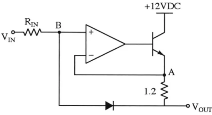
The IO Connector was the first successful printed circuit board design that addressed the issues stated in Chapter 1 and the goals mentioned above. The connector included a custom power supply that offered an output voltage supply of only +1OVDC, ca-pable of delivering up to one amp of current. The power supply design consisted of a Fairchild KA334 operational amplifier, a Fairchild TIP31 NPN power transistor (able to deliver up to 3A of current), and a diode, all connected in a topology similar to a linear voltage regulator configuration (Figure 2-1).
Initially, the operational amplifier pegs the voltage at node A near 1OV, and at low currents, VOUT is also kept at 1OV. The diode is off at low currents, but as the current
demand increases towards 0.5A, the voltage at node A increases and the diode starts to exponentially turn on. As higher currents are drawn from VOUT, more current is conducted through the diode. This causes the voltage at nodes A and B to drop, due to the operational amplifier trying to keep its inputs equal. Since the voltage at node
A drops, VOUT must also drop since it is linked to A via the 1.2Q resistor. This is
how the intrinsic, though non-intuitive, current limiter works. Figure 2-2 illustrates the relationship between output voltage and output current of this design.
+12VDC RIN B VIN A 1.2 hJ Vour
Figure 2-1: Core circuit configuration of the IO connector.
IV Characteristic of +1OVDC 10 9 .5 0 6 5 0 0.1 0.2 0.3
Output Current [A] 0.4 0.6
Figure 2-2: Characterizing the output voltage versus output current of the 10 Con-nector's
+1OVDC
supply rail.2.2
Power Supply Interface Design
The final design of the interface (Figure 2-3), centers around two power modules that offer a complete solution in a small, low profile Quad Flat No-leads (QFN) package [4]. The 12V battery in the robot feeds into both these modules to create a positive and negative 8V power rail. The positive 8V is created by the TPS84250, which combines a 2.5A DC-DC buck converter with an internal inductor. Similarly, the
TPS84259 creates the negative 8V rail using a 2A DC-DC buck converter with an
internal inductor.
The TPS84250 and TPS84259 chips contain inductors, which eliminates the effort and space needed to include an external inductor on the board. Both modules are 9mm by 11mm packages, which only consume 1.6% of the 96.5mm by 63.5mm printed circuit board. Since the modules have a small footprint and require a minimal number of passive components, they do not dissipate much heat, foregoing the need to use external heat sinks.
WDC
+12V TPS8250 +
VIN VOUT
e
CN RvLo, RET COUT CoUt
.1 UVLO VADJb SSrTR RTl CT STSEL AGND PGND R -8VDC CoUT U CW2
Figure 2-3: Schematic of the power supply interface consists of two DC-DC power converter modules, followed by a set of low dropout regulators. The
+12VDC
input is a direct connection from the batteries.TS7A4700 +7VDC SVIN VOUT CIN d
b
OUT NR GNDI ,-C 8PV 1P6V 3P2V TPS7A3301 -7IVDC VIN VouT ENT FBT fRTCU NRISS +12V TPS842S9 CVIN VLo -UVLO k_VOUr RvvL2 RT MTEL VADJFollowing the DC-DC power converter modules are a set of low dropout regulators (LDO) that regulate the output voltages at +7V and -7V and are able to supply up to one amp of current. The purpose of these linear regulators is to filter out the output voltage ripple that is inherent to all DC-DC switching converters so that the board can present stable and clean rails to the student boards.
2.2.1
Positive Voltage Branch Parameters
The TPS84250 is a power module designed by Texas Instruments and, depending on its input voltage, is capable of providing output voltages from +7V up to +50V, while providing up to 2.5A of current. According to the datasheets [2], the three primary parameters that must be selected when designing with the TPS84250 are the output voltage, undervoltage lockout (UVLO) threshold, and the switching frequency.
The output voltage was chosen to maximize the power supply rails given the input constraints imposed by the robot's batteries and the allowable minimum input voltage supported by this module. The TPS84250 supports a minimum input voltage of 7V or (Vat + 3V), whichever is largest. Since the battery must be kept above the
robot's shutdown voltage of 11V, the minimum input voltage was chosen to be 11V. In other words, the output voltage used was
+8VDC.
Physically, a resistor Rser sets the output voltage by completing an internal voltage divider that feeds back a sensed portion of the output voltage [2]. By setting RSET to 90.9kQ, the output voltage is fixed at +8VDC. The Undervoltage Lockout (UVLO) threshold determines the input and output voltage threshold where the module activates and deactivates power conversion. It is recommended to set the UVLO threshold to approximately80-85% of the minimum input voltage. To set the UVLO threshold, two resistors are
chosen by the following equations:
RuvLo1 = (VON - VOFF) )(2.1)
2.9- 10-3 1.25 RUVLO2 = - 1.25 -
(kQ)
(2.2) (ON-1.25) + (0.9 . 10-3) RUvLO1Raising the switching frequency significantly improves various performance as-pects of the module. It reduces the output voltage ripple, increases the efficiency of conversion and improves the transient response of the module. A switching frequency of 600kHz was used.
2.2.2
Negative Voltage Branch Parameters
The TPS84259 is also a power module designed by Texas Instruments [1], capable of providing output voltages from -3VDC to -17VDC. Unlike the TPS84250, the negative power module is only capable of providing up to 2A of current, but like the TPS84250, the same three primary parameters apply when designing with the
TPS84259: output voltage, UVLO threshold and switching frequency.
For purposes of symmetry, an output voltage of -8VDC was chosen. Similarly, by completing an internal voltage divider with RSET equal to 90.9kQ, the output voltage was fixed at -8VDC. For the UVLO threshold, the two resistors were chosen by the following equations: 0.5
(kQ)
(2.3)RUVLol
= 2.9.0-3
ft 1.25 RUVLO2 = oN-.25) (kQ) (2.4) RuvLO1 + (0.9 - 10-3)For the switching frequency, the TPS84250 only offers two frequencies, 500kHz for input voltages above +18V and 800kHz for input voltages below
+18V.
Since the battery voltage falls under 18V, a switching frequency of 800kHz was used.2.2.3
Reducing Ripple
DC-DC converters employ switches to create a periodic signal whose average voltage
can be modulated and a filter to ideally remove all frequencies except the average voltage, commonly known as DC. Due to the dynamic switches and the unfeasibility of building an ideal filter, DC-DC buck converters always have a small ripple riding
on top of the average voltage. There are various approaches to minimizing this output voltage ripple. To mitigate this effect, an additional capacitor or a more extensive filter can be placed at the output of the converter. Another solution would be to follow the power module with a low dropout voltage regulator. Table 2.1 below, was adapted from Texas Instruments' Application Report SLVA549 [31 and it summarizes the peak-to-peak ripple that should be expected given a certain output filter solution.
Table 2.1: Output Filter Solutions
Output Filter VP
2 x 47 pF ceramic capacitors 21 mV 4 x 47 pF ceramic capacitors 12 mV 2 x 47 piF ceramic caps + -x filter 2.9 mV
2 x 47 pIF ceramic caps + LDOs 3 mV
To minimize the peak-to-peak voltage ripple, ultralow-noise linear voltage regu-lators (TPS7A4700, TPS7A3301) were placed after the power modules. The voltage regulators not only deliver clean voltage rails to the student circuits, but would also help regulate the output voltage. They are also capable of sourcing up to one amp of current, which is enough to support the transient current required by the Lego motor. The output voltage ripple is also dependent on the value of the output capaci-tor, its equivalent series resistance (ESR) and the switching frequency of the power modules. To maximize performance, capacitors with low ESR were used when ap-propriate.
2.3
Layout Considerations and Construction
The circuit board was laid out using the commercial program ExpressPCB on a 96.5mm by 63.5mm board, the maximum size that fits inside the Pioneer robot. Apart from the size constraint, another significant factor considered when laying out the modules was the thermal stress of the design.
dissipate heat into the PCB and not require any additional heat sinks. The copper on the board must be able to withstand the thermal dissipation put off by the modules under normal operation. Also, as the battery powering the board discharges, the input voltage declines, creating a larger difference between the input and output voltages. This voltage difference generates more heat that must be removed efficiently. Planes large enough that connect various circuit nodes must be used to conduct heat way from the components and into the environment. There is a trade-off to how large the planes can be, though, since the melting ease of the solder will also be affected. When initially placing the components on the printed circuit board, sufficient heat must be used to melt the solder to attach the components. If the planes are too large, heat will leak away from the desired solder joint area and so not enough heat will gather locally. Low heat results in cold solder joints, where the components are not well attached to the board and are easily broken, causing massive board failure.
The size of the particular components determines how easily they can be handled and soldered on the printed circuit board. Even though a smaller component package could be used to save more board space, such as 0402 (1mm x 0.5mm), soldering it on the board can be more difficult.
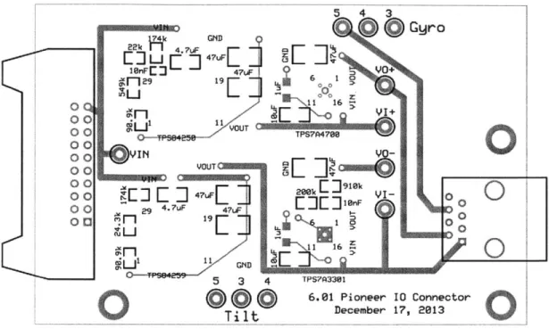
Since the power supply board must be able to sustain an output up to 1A, PCB traces that carry this significant amount of current must be wider than signal traces. Current-carrying traces were sized to be 1.27mm, enough to carry 2A. The wider traces can be noted in Figure 2-5, which shows the final layout of the bottom layer. Connecting the battery to VIN is one example of a wider trace. Such traces, along with the size of the planes, can be seen in Figure 2-6, which shows the final layout of the top layer of the fabricated card.
00 00 00 00 5 4 k GNDGyro
E]
47uFE
I
nFE] 47uF i:; LO+9
19
-- 6 119[ 000
11
1I1
0
OVIN
Figure 2-4: Bottom layer of the layout for the power supply interface board.
,,qhI OIN
il
.7uF TPS8429 O 5 4 3Gyro
VO+
TPS?P4780I~
*1 TPS7A338I 6.61 Pioneer0
Connector Tilt December 17, 2013Figure 2-5: Top layer of the layout for the power supply interface board.
C
00 00 00 00 00 00 00 00 00 00 YOUTL
Ja....____ 00 00EJ
E]47uF~
2SE kI 00 3 4.7uF 47uFan 0 00Y
00
1
1 1LJ 11 C,~E.' 3 4 TPs33016
6.01 Pioneer I ConnectorTilt
December17,
213 __jChapter 3
Evaluation
Measurements were gathered from a series of tests designed to characterize the custom power supply interface. The tests included analyzing the content of the DC signal
by taking its Fourier Transform using a Tektronix TDS3034B oscilloscope to show its
frequency spectrum, along with tests to determine performance parameters such as line and load regulation.
3.1
Load Regulation
In general, the voltage of a circuit node often decreases as it delivers an increasing amount of current to its attached load. This characteristic is expected from most circuit topologies that focus mainly on signal conditioning, such as signal amplification or filtering. For DC-DC converters, though, the voltage supplied by the converter must ideally remain constant at its desired level, independent of its load. Since this is not physically possible, the performance parameter that quantifies the converter's ability to maintain a constant output voltage under varying load conditions is known as load regulation and is defined as:
AVat
Load Regulation = (3.1)
Once the power supply rails cannot sustain the current demanded by the load, the voltage will start to drop. In other words, the load through its current demand regulates the output voltage. Ideally, load regulation should approach zero for the board as this means that the output voltage stays constant regardless of load.
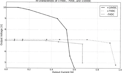
The power supply interface card was tested for load regulation by connecting a variety of high-wattage resistive loads across the output leads of the card. The output voltage was then measured with a Tektronix TDS3034B oscilloscope. For comparison, the +10VDC 10 connector had its load regulation characterized in the same setup as well. Figure 3-1 plots the output voltage against the output current of
+7VDC
and+10VDC rails, along with the magnitude of the -7VDC rail.
IV Characteristic of +7VDC, -7VDC, and +10VDC 10 9 6L 5 0.- 0. 4 0.6
Output Current [A]
0.8
Figure 3-1: Comparing IV Characteristics of +10VDC, +7VDC, of -7VDC.
1.0
and the magnitude
Each supply rail manages to stay fixed at its desired output voltage for low cur-rents, but start to fall at higher current demands. The +10VDC supply on the original card drops an entire volt, down to
+9VDC,
when the output current reaches 0.5A and continues to drop exponentially. Similarly, the +7V supply rail on the new card exponentially drops at higher current demands, but stays fixed at or near+7V
at- +10VE +7VD - - -7VDC -~~ -... ...---DC
0
0.2higher current demands compared to the
+10V
supply rail. The -7V supply rail also performs better than the+10V
rail but falls short when compared to the+7V
rail since the output voltage dives significantly when the output current reaches 0.7A. It is important to note that none of the designs managed to reach IA as stated in the electrical specification in Chapter 2.3.2
Line Regulation
Another performance parameter determined was line regulation, which measures the sensitivity of the output voltage to variations in the power supply's input voltage. For example, the input voltage starts to fall as the battery drains throughout the robot's operation. For a constant output current, line regulation is defined as follows:
AVw
1Line Regulation = (3.2)
AVin
Like load regulation, this specification should ideally also approach zero for the power supply interface board. Line regulation was determined by connecting the board to a varying power supply, while measuring the output voltage. For small output currents (below 0.5A), the board kept the output voltage at +7VDC and -7VDC down to an input voltage of 10.5V, well below the 11V battery voltage that would cause the robot to go into shutdown mode.
3.3
Signal Quality
One of the main goals of this thesis was to create a power supply interface that could deliver clean, fixed bipolar DC voltage levels that could power student circuits. The quality of the DC signal provided by the board is better understood by measuring the frequency content of the supply rails. The expectation is that most of the signal energy resides at DC (zero frequency) while other frequencies are attenuated. This expectation translates to the time domain as steady, constant voltages with negligible ripple.
Both the +8VDC and -8VDC are the voltage outputs of the DC-DC converters, TPS84250 and TPS84259, while the +7VDC and -7VDC are the outputs of the linear regulators, TPS7A4700 and TPS7A3301. Using a Tektronix TDS3034B oscilloscope, the FFT was taken of the supply voltages using a preprogrammed Hamming window-ing function. The signal energy was measured from 0Hz to 2.5MHz for the followwindow-ing voltages: +7VDC, -7VDC, +8VDC, and -8VDC (Figure 3-3, Figure 3-4).
From the spectrum shown in Figure 3-3, there is significant energy at DC (OHz) while the majority of higher frequencies are suppressed below -40dBV or 10mV. The
+7V
rail is actually at 7.08V (17dBV) and the -7V is almost symmetrical with a magnitude of 7.04V (16.85dBV).To determine if the linear regulators helped in decreasing the ripple on the DC voltage coming out of the DC-DC converters, the frequency content of the
+8VDC
and -8VDC was also measured. Again, most of the signal energy was present at DC(OHz) while the higher frequencies were suppressed below -40dBV. The
+8V
rail was measured at 8.2V and the -8VDC rail was measured at -8.1V.FFT of +7VDC ... .. .. ... .-20 FFT of -7VDC 10 - 0- 10-20 30- 40-50 ____mi iiIi 500000 1000000 1500000 Frequency [Hz] 2000000 2500000
Figure 3-2: Comparing Fourier Transform of
+7VDC
and -7VDC.FFT of +8VDC
FFT of -8VDC
500000 1000000
Frequency [Hz]
1500000 2000000 2500000
Figure 3-3: Comparing the Fourier Transform of
+8VDC
and -8VDC. 10-0
-10 (U -20 01-30 -40 C -M 0 10 > 0 -10 -20 -30 2-40 -S0 20 10 -10 -20 30 -40 -50 0Chapter 4
Discussion
In the measurements performed on the power supply interface, the general observa-tion is that the board successfully presents the appropriate bipolar DC voltages for most current demands; however, the board does fall short of providing one amp of output current. In this chapter, the results of the board performance presented in Chapter 3 are discussed in depth and in the context of the goals stated in Chapter 2: physical constraints, ease of construction, electrical specifications, and circuit design complexity.
4.1
Electrical Specifications
To summarize, the electrical specifications set constraints on both the desired output voltage and current. The magnitude of the output voltage was to be within the standard range of 5VDC to 12VDC, while the output current had to support and be limited to IA.
4.1.1
Load Regulation
The power supply interface was designed to deliver up to one amp of current without the output voltage falling significantly from its desired level. Once the current demand surpasses one amp, the voltage must drop quickly for the safety reasons mentioned in
Chapter 1. From Figure 3-1, none of the supply rails, including the previous
+1OVDC
design, managed to output IA. The+10VDC
rail begins to exponentially decrease after 0.5A, while the -7VDC pushes the limit to 0.65A before falling abruptly. The+7VDC
rail performed the best, keeping the output voltage at 7V up to a current of0.9A.
To understand the reason behind the current limitation, Figure 4-1 illustrates the maximum output current (or safe operating current) possible for both DC-DC con-verter modules, TPS84259 and TPS84250. Extrapolating for VIN = 12V and VOUT = 8VDC, the maximum output current hovers around IA. When the low dropout linear
regulators (TPS7A4700, TPS7A3301) in the next stage need to source an output of
IA, the required current input to the regulators would have to be larger than IA,
which is not possible.
Safe Output Current for Different Magnitudes of Vout
- - Vout = 3.3V 2.5- Vout = 5V Vout = 9V * Vout = 12V Vout = 15V 2.0-. --- - - - - - -2 .0 . . ... . 8 8 10 2 14 16 18 20 Input Voltage [V]
Figure 4-1: Maximum Output Current of the TPS84259 and TPS84250 power mod-ules, for different magnitudes of output voltages. Plot adapted from SOT chart given on TI website.
Even though the new power supply interface could not sustain a fixed voltage for the specified current range, it did surpass the previous design's current capacity. The
10 connector's
+10VDC
supply was capable of driving the Lego motor without a problem, and the new power supply interface managed to do so as well.4.1.2
Line Regulation
The board was able to keep the output voltage fixed at the desired levels, even when the input voltage dropped down to 10.5VDC. As mentioned in Chapter 2, the robot will enter the shutdown mode when the batteries drain below the programmed input voltage of +11VDC. Since the board can sustain the output voltage well below the programmed shutdown voltage, the robot will be able to provide the proper functionality until it is forced to switch off.
4.1.3
Signal Quality
Another aspect of the electrical specification that was put forth in the design phase was to create a clean DC signal with negligible ripple. Having significant ripple on top of a signal can cause unwanted effects in circuits. The spectrum shown in Figure 3-3, indicates that there is significant signal energy at DC (OHz) while other frequencies are suppressed below -40dBV. Mapping these measurements over to the time domain gives a ripple of less than 10mV, superimposed on top of the desired dc-signal for all supply rails. The expected ripple given in Table 1 of Chapter 2 was approximately 3mV, which follows well with the measurements.
Interestingly, the signal frequency content out of the converters was similar to that out of the low dropout regulators. The purpose of including linear regulators was to help decrease the ripple further; however, the measurements indicate that the amount of ripple suppression was negligible. The extra capacitors placed at the outputs of the power modules may be the reason. Since the power modules are rated to source up to about 2A (depending on input and output voltages of the power modules), the low dropout regulators may not be necessary to include in the design.
4.2
Circuit Design Complexity
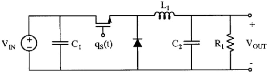
Producing a positive output voltage on a printed circuit board is a straightforward endeavor using common DC-DC converter topologies; however, creating a stable nega-tive output voltage may require more complexity and design expertise. Some discrete circuit design approaches that solve this problem include using a buck converter (Fig-ure 4-3), a switched-capacitor based design (Fig(Fig-ure 4-4), an indirect DC-DC converter (Figure 4-6), and a flyback converter (Figure 4-7).
VW
T
C1 qs(t) C2 R, VourFigure 4-2: DC-DC Buck Converter
(t)
DT T T+DT 2T
t
Figure 4-3: Timing diagram for both the Buck and Indirect Converter, where T is the period and D represents the duty cycle, or the fraction of T that the switch is on.
The switched-capacitor design requires a charge pump stage, along with a con-troller that helps regulate the output voltage. For example, a simple voltage inverter (Figure 4-4) can be used to create a negative voltage (V., = -Vi,). Despite only using two capacitors, it is clear that the switches must follow a strict timing scheme (Figure 4-5) in order to not lose charge stored. To implement the timing scheme, extra support circuitry, such as a microcontroller, would be required.
q1(t)
2)-q1(t) q2(t)
Figure 4-4: Charge Pump voltage inverter design, where VOUT = -VIN
q1(t)
DT T T+DT 2T
q2(t)
I I--
----
-t
DT T T+DT 2T
Figure 4-5: Timing diagram for Switched Capacitor Design, where T is the period and D represents the duty cycle, or the fraction of T that the switches are on.
Another way to create the negative power supply would be to build a buck-boost (indirect) DC-DC converter (Figure 4-6), where an inductor is used as an intermediate energy transfer agent between the input and output ports. The desired output voltage can then be controlled based on the duty cycle represented by D in the following equation:
- = -
D
(4.1)Vin 1 - D
The drawback to using this design is primarily that it requires the use of an inductor. Inductors can take up valuable space on the board and are often leaky.
_
T)J
VIN
TCe
qs(t)
I
+
7
21
R,
VOUT
Figure 4-6: Buck-Boost (Indirect) Converter that follows the timing in Figure 4-3.
In a similar vein, the flyback converter (Figure 4-7) uses a transformer in addition to an inductor. The transformer adds another design degree via isolation and the number of windings (NI: input-side number of windings, N2: output-side number
of windings) for maximum flexibility for a desired output voltage as shown by the following equation:
Vo D N2(4.2)
Vin 1
- D
N1Unfortunately, the design still uses an external inductor, while the transformer is large and suffers from leakage as well.
VIN
Isn-C1=i R1i
Figure 4-7: The Flyback Converter utilizes a transformer.
Fortunately, as on-chip designs have scaled tremendously over the years, there has been an increase in the number of available DC-DC converting power modules that offer all the above designs in a compact and convenient package [4]. For example, the TPSO400 is a design based on a charge pump inverts the input voltage without
the need of using an inductor and is capable of delivering a maximum output current of 60mA. The TPS5430 is a buck-boost circuit that creates a negative voltage with the use of an external inductor, while the TPS54060 is also a buck-boost circuit but coupled with a transformer to create a bipolar rail design.
Taking advantage of the power modules and low dropout voltage regulator avail-able, a simple two-stage design for each of the positive and negative voltage branch was chosen to minimize the circuit design complexity. Each branch was composed of a power module to convert the 12V battery to a desired output voltage, followed
by a linear regulator to regulate the output, keeping the DC signal quiet and clean
(minimizing ripple).
4.3
Physical Constraints and Ease of Construction
The completed power supply interface was laid out on a 96.5mm by 63.5mm printed circuit board, which met the goal of fitting inside the robot. Since the robot must remain mobile and power the student circuits simultaneously, it was vital that the power supply interface fit well without hindering the other circuitry internal to the robot. The use of IC circuits such as the power modules and low dropout regulators helped eliminate the need for external inductors, transformers, or large heat sinks.
A small number of external resistors and capacitors were necessary to set the IC
modules.
There was a trade-off between the size of the board and its components with the ease of constructing the final power supply interface. Some planes and traces on the PCB were not strategically sized or placed. In pursuit of saving space, some components were placed close to the power modules, making it difficult to solder between components. During the testing phase, a power module failed. Removing this component without accidentally removing the surrounding components proved to be difficult.
4.4
Pedagogy
As mentioned in Chapter 1, students often struggle to understand why it is necessary to create a buffered
+5VDC
reference for the bidirectional controller of the head. In order to obtain the correct head behavior using the+1OVDC
supply, it is vital for students to connect a buffered+5VDC
to the M- lead as shown in Figure 4-8. To help students experiment with engineering design, the focus should be on developing a variety of circuits that connects the right (VR) and left (VL) photodiode "eye" voltages to the M+ lead in a way that results in the correct behavior.+1OV
VRR VR RR2M Vx + R VLR
R2 VxFigure 4-8: Under the 10 connector's unipolar +1OVDC, the circuitry for motor rotation requires a buffered
+5VDC
mid-rail voltage.Replacing the unipolar power supply with the new bipolar power supply interface, all the +5VDC nodes are shifted to OV, as shown in Figure 4-9. The entire circuit that was connected to the M- lead is eliminated, along with simplifying equations 1.1 and 1.2 as expected:
VM+ > OV; rotate right (4.3)
VM+ < OV; rotate left (4.4)
With the +5VDC bias confusion out of the way, students will have much more time to experiment with different circuits and build better intuition about design.
R2
RW
VR M+ MVL
R,
R2Figure 4-9: Under the board, a bipolar 7VDC supply eliminates the need for a buffered
+5VDC
mid-rail voltage by setting the nodes previously using the+5VDC
voltage to OV. Students can then focus on designing the circuitry that connects to the M+ lead of the motor.Chapter 5
Conclusion
5.1
Thesis Summary
This thesis discussed the design and implementation of a custom power supply in-terface for the Pioneer mobile robot. The purpose of the inin-terface was to provide a bipolar power supply of magnitude 7VDC, allowing students learning electronics to focus more on circuit design rather than on tangential problems.
The custom power supply interface successfully delivered a bipolar voltage supply of
+7VDC
and -7VDC. Even though it was not able to regulate this voltage when the current demand neared lA, it was still able to provide quiet power supplies for a larger range of currents than the currently used IO connector. The module-based design turned out to be highly suitable for our goals.Unfortunately, more thorough testing was needed before fully determining if this power supply interface could replace the 10 connector. Since the purpose of this thesis was to explore the additional feature of bipolar voltage supplies, this design iteration of the board did not include the DAC circuitry that allows communication between the robot and a laptop. Such circuitry would allow for long-term dynamic tests. For example, running the board such that the head would continuously move right and left would help make sure that the board could sustain the necessary output current for long periods of time.
5.2
Suggestions for Future Designs
Even though much of the core design has been designed and tested, there is still further work to be done. As mentioned above, combining the design of this thesis with the already working DAC circuitry from the current 10 connector would help run long-term dynamic tests to make sure the board can sustain loads for hours without overheating or breaking down.
The power modules include current limiters inside so when an overcurrent condi-tion is encountered, the output current is limited and the output voltage is reduced. To help protect the power supply interface and students further, including an explicit fuse at the board outputs would be a welcome addition.
Finally, in the next iteration of the board, the layout can be improved by smaller connections between the passive components and large planes. The planes were used to help dissipate heat from the power modules, but they do not thermally help the passive components very much. By using thinner traces from the components to the planes, soldering the board would be easier.
By adhering to these suggestions, the next iteration of the power interface supply
will be one step closer to replacing the current 10 connector and students will be able to benefit greatly by having access to a bipolar voltage supply.
Appendix A
Schematics
+8VDC
TPS7A4700
+7VDC
0
1
VIN VOUT CIN-1EN SENSE CU NR GND OP8V 1P6V 3P2VFigure A-1: TPS7A4700 by Texas Instruments
Table A.1: Component values used for the TPS7A4700.
CIN 4.7 pF COUT 47 pF
-8VDC
TPS7A3301
VIN VOUT CNT EN FB NR/SS C4 GND CFFFigure A-2: TPS7A3301 by Texas Instruments
Table A.2: Component values used for the TPS7A3301.
CIN COUT CFF CNR
R
1 R2 10yF
47 pF 10 nF 1 yF 910 kQ 183 kQ-7VDC
COU7+8VDC
COUT1OUT2
+12V
TPS84250
0
C N UV OIVIN VOUT R~ UVLO VADJ 1 Css /LK[ RRT STSEL AGND PGNDFigure A-3: TPS84250 by Texas Instruments
Table A.3: Component values used for the TPS84250.
CIN COUT1 COUT2 Css RuVLO1 RuVLo2 RSET 4.7 pF 47 pF 47 pF 10 nF 174 kQ 22 kQ 90.9 kQ 549 kQ
+12V
CINj RuvLoi RUVL02TPS84259
VIN VOUT VOUTPT UVLO AVOUT RT STSEL VADJ GND-8VDC
Couri CoUr2Figure A-4: TPS84259 by Texas Instruments
Table A.4: Component values used for the TPS84259
CIN 4.7 yF COUT1 47 pIF COUT2 47 piF RuvLol 174 kQ RuVL02 24.3 kQ RSET 90.9 kQ
Appendix B
Layout
5 4 3 MMMMM 5 Gyro 174k GD 22LC M47uF 1 UnFE 47 F9
: "+
fl29 19 60 1 1 1V IU GLJUIII u your VOUT ]E 47uFL 29 4.7uF 47uFfl
19Eri
LU1 II GHlD 5 3 TiltE 3
J9b 2JEEInF
0. A TPs7A3301 6.01 Pioneer ID Connector December 17, 2013Figure B-1: Bottom layer of the layout for the power supply interface board.
a 0OQ 00 00 00 00 00 00 00 00 00 C I N (U
0
LQ
C
I I 40
ICYIN -97uF
alf
TPS842590
5 4 30Gyro
VO+VI+
TPS7A470 *F i0 900 611110e
____
TPS7A3301 6.01 Pioneer I Connector December 17, 2013Figure B-2: Top layer of the layout for the power supply interface board.
5 4 3 VIN 174kc GND 22k M 4.7uF
ENE
M
El4741rF[:
3 47 F j rO129M 250 L TPSa19 TPS84250 V) TPs7A4700 *VIN VOUT :R~ ] N0 4 7 uF r 1 2, 4.7uF 47uF --s GD TPS84259 YUyr
I 0 3. y0+ I+ y0-6 11411 NI 3ekE n~e I EnEEIrFA I--111 NW 3.lil 5 3 4 TPS7A3301 Tilt 6.01 Pioneer 10 Connector December 17, 2013Figure B-3: Top layer of the layout for the power supply interface board with planes removed to show specific chip layout.
00 00 00 00 00 00 00 00 00 00
K
-@ 00e --.. 0 0.*
Bibliography
[1] Texas Instruments.
4.5-
V to40-
V Input, 15- W, Negative Output, Integrated Power Solution. TPS84259 datasheet, August 2012 [Revised June 2013].[2] Texas Instruments. 7- V to 50- V Input, 2.5-A Step-Down, Integrated Power Solu-tion. TPS84250 datasheet, August 2012 [Revised June 2013].
[3] Texas Instruments. Reducing Output Ripple and Noise with the TPS84259.
TPS84259 Application Report, November 2012.
[4] Rich Nowakowski. Techniques For Implementing a Positive and Negative Output Voltage for Industrial and Medical Equipment. Available at http: //ww. ti. com/ lit/ml/szzn001/szzn001.pdf.