Publisher’s version / Version de l'éditeur:
Journal of Lightwave Technology, 29, 12, pp. 1790-1796, 2011-06-03
READ THESE TERMS AND CONDITIONS CAREFULLY BEFORE USING THIS WEBSITE. https://nrc-publications.canada.ca/eng/copyright
Vous avez des questions? Nous pouvons vous aider. Pour communiquer directement avec un auteur, consultez la première page de la revue dans laquelle son article a été publié afin de trouver ses coordonnées. Si vous n’arrivez pas à les repérer, communiquez avec nous à PublicationsArchive-ArchivesPublications@nrc-cnrc.gc.ca.
Questions? Contact the NRC Publications Archive team at
PublicationsArchive-ArchivesPublications@nrc-cnrc.gc.ca. If you wish to email the authors directly, please see the first page of the publication for their contact information.
Archives des publications du CNRC
This publication could be one of several versions: author’s original, accepted manuscript or the publisher’s version. / La version de cette publication peut être l’une des suivantes : la version prépublication de l’auteur, la version acceptée du manuscrit ou la version de l’éditeur.
For the publisher’s version, please access the DOI link below./ Pour consulter la version de l’éditeur, utilisez le lien DOI ci-dessous.
https://doi.org/10.1109/JLT.2011.2141974
Access and use of this website and the material on it are subject to the Terms and Conditions set forth at
Silicon-chip-based real-time dispersion monitoring for 640 Gbit/s DPSK
signals
Vo, Trung D.; Corcoran, Bill; Schroder, Jochen; Pelusi, Mark D.; Xu,
Dan-Xia; Densmore, Adam; Ma, Rubin; Janz, Siegfried; Moss, David J.; Eggleton,
Benjamin
https://publications-cnrc.canada.ca/fra/droits
L’accès à ce site Web et l’utilisation de son contenu sont assujettis aux conditions présentées dans le site LISEZ CES CONDITIONS ATTENTIVEMENT AVANT D’UTILISER CE SITE WEB.
NRC Publications Record / Notice d'Archives des publications de CNRC:
https://nrc-publications.canada.ca/eng/view/object/?id=0f068f69-b397-49dc-8f20-ed96f7d4ae68
https://publications-cnrc.canada.ca/fra/voir/objet/?id=0f068f69-b397-49dc-8f20-ed96f7d4ae68
Silicon-Chip-Based Real-Time Dispersion
Monitoring for 640 Gbit/s DPSK Signals
Trung D. Vo, Bill Corcoran, Member, IEEE, Jochen Schröder, Mark D. Pelusi, Dan-Xia Xu, Adam Densmore,
Rubin Ma, Siegfried Janz, David J. Moss, Senior Member, IEEE, Fellow, and Benjamin J. Eggleton, Fellow
Abstract—We demonstrate silicon-chip-based instantaneous
chromatic dispersion monitoring (GVD) for an ultrahigh
band-width 640 Gbit/s differential phase-shift keying (DPSK) signal.
This monitoring scheme is based on cross-phase modulation in
a highly nonlinear silicon nanowire. We show that two-photon
absorption and free-carrier-related effects do not compromise
the GVD monitoring performance, making our scheme a reliable
on-chip CMOS-compatible, all-optical, and real-time impairment
monitoring approach for up to Terabit/s DPSK signals.
Index Terms—Nonlinear optics, optical performance monitoring
(OPM), optical planar waveguides, optical signal processing,
spec-tral analysis.
I. I
NTRODUCTIONN
onlinear silicon photonics has attracted significant
atten-tion in recent years due to major advances in
nanofab-rication enabling a wide range of applications on integrated
silicon-on-insulator (SOI) photonic circuits [1]. Another major
motivation behind the interest in nonlinear photonic nanowires
is the improved energy efficiency of nonlinear processes due
to the significant enhancement of the nonlinear response
(where
and
are nonlinear index and
effec-tive mode area, respeceffec-tively), which is up to 5 orders of
mag-nitude larger than in silica fiber [2]. These advantages make
silicon an attractive nonlinear platform for on-chip all-optical
signal processing, and there have been numerous impressive
demonstrations, including all-optical switches [3], format
con-Manuscript received November 29, 2010; revised March 04, 2011; accepted March 31, 2011. Date of publication April 11, 2011; date of current version June 03, 2011. This work was supported in part by the Australian Research Council (ARC) through its ARC Centres of Excellence and Linkage Programs with Finisar Australia.
T. D. Vo, J. Schröder, M. D. Pelusi, D. J. Moss, and B. J. Eggleton are with the Centre for Ultrahigh Bandwidth Devices for Optical Systems, In-stitute of Photonics and Optical Science, School of Physics, University of Sydney, Sydney, N.S.W. 2006, Australia (e-mail: trungvo@physics.usyd. edu.au; j.schroeder@physics.usyd.edu.au; m.pelusi@physics.usyd.edu.au; dmoss@physics.usyd.edu.au; egg@physic.usyd.edu.au).
B. Corcoran was with the Centre for Ultrahigh Bandwidth Devices for Optical Systems, Institute of Photonics and Optical Science, School of Physics, Univer-sity of Sydney, Sydney, N.S.W. 2006, Australia. He is now with Chalmers Uni-versity of Technology, Gothenburg, Sweden (e-mail: billc@physics.usyd.edu. au).
D.-X. Xu, A. Densmore, R. Ma, and S. Janz are with the Institute for Microstructural Sciences, National Research Council, Ottawa, ON K1A-OR6, Canada (e-mail: Dan-xia.Xu@nrc-cnrc.gc.ca; Adam.Dens-more@nrc-cnrc.gc.ca; Rubin.Ma@nrc-cnrc.gc.ca; siegfried.janz@nrc-cnrc.gc. ca).
Color versions of one or more of the figures in this paper are available online at http://ieeexplore.ieee.org.
Digital Object Identifier 10.1109/JLT.2011.2141974
version [2], tunable delay and optical phase conjugation [4],
[5], time-division demultiplexing [6], [7], ultrafast waveform
measurement [8], wavelength conversion [9], [10], Raman laser
[11], [12], light amplification [13], [14], and optical
impair-ment monitoring via slow-light enhanced third harmonic
gen-eration [15].
Recently, we have exploited cross-phase modulation (XPM)
[16] in a nonlinear waveguide to capture the radio frequency
(RF) spectrum of an ultrahigh bandwidth optical signal [17].
This scheme has been used to characterize terabit/s data [18],
[19] as well as multi-impairment monitoring of high-bit-rate
in-tensity-encoded [20], [21] and phase-encoded signals [22]. Our
initial experiments were reported in chalcogenide glass
pho-tonic integrated circuits. Besides chalcogenide, silicon would
be a natural platform to consider for this scheme because of
the mature CMOS fabrication process; however, silicon
suf-fers from relatively high two-photon absorption (TPA),
pho-togenerated free-carrier absorption (FCA) and phopho-togenerated
free-carrier dispersion (FCD) when operating at
telecommuni-cation wavelengths [23]–[25]. The TPA and FCA are nonlinear
losses, which reduce the efficiency of the XPM process, while
FCD modifies the material refractive index and can distort the
modulation caused by the Kerr nonlinearity [26], [27]. This may
result in reduced device efficiency and a cross-chirp that can
distort the Kerr-based XPM and lead to errors in the RF
spec-trum in our optical performance monitoring (OPM) method. We
recently demonstrated that TPA and free-carrier effects are
in-significant at the power used for the RF spectrum monitoring of
640 Gbit/s ON–OFF keying signals [19], [28].
In this paper, we report on the first demonstration of a
sil-icon-chip-based OPM scheme to instantaneously monitor
dis-persion of ultrahigh bandwidth phase-encoded signals. We
ex-ploit the ultrafast effect of XPM in a CMOS compatible silicon
nanowire, in combination with a simple optical bandpass filter
(BPF) and a relatively slow (
s response time) power meter
to continuously monitor the group velocity dispersion (GVD)
for a 640 Gbit/s return-to-zero differential phase-shift keying
(RZ-DPSK) signal. As the fluctuations of GVD in optical
com-munication links typically occur on times scales much greater
than microseconds, this scheme allows for real-time monitoring
of GVD. We numerically investigate the impact of TPA and
free-carrier related effects and demonstrate that they do not
af-fect performance of GVD monitoring. The potential integration
of electronics with our CMOS compatible device offers the
pos-sibility for the creation of a terahertz bandwidth [28], low-cost,
chip-based, real-time OPM device.
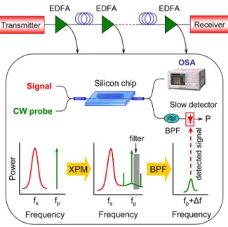
Fig. 1. Conceptual diagram of silicon-chip-based instantaneous GVD moni-toring. This scheme is suitable to be operated at nodes, after in-band EDFA in reconfigurable networks.
II. W
ORKINGP
RINCIPLEFig. 1 shows a schematic of all-optical performance
moni-toring using a silicon-chip-based RF spectrum analyzer. When
the signal under test (SUT) and a continuous wave (CW) probe
are copropagated through the nonlinear waveguide, the probe’s
phase is modulated via XPM [16]. The broadened spectrum
around the probe frequency is proportional to the power
spec-trum of the input signal intensity waveform if the maximum
cross phase-shift on the probe
, where
and
are the signal peak power and effective length of
a waveguide, respectively [29]. Note that this monitoring
ap-proach is suited for operation at nodes [after in-line
Erbium-doped fiber amplifiers (EDFAs)] of reconfigurable optical
com-munication networks to obtain sufficient input power.
The key device used in the experiment is a 1.5 cm long
SOI nanowire. The waveguide is 450 nm wide by 260 nm
thick, producing an effective transverse electric (TE) mode
area
0.15 m , as extracted from finite element method
mode solver (RSoft FEMsim) calculated using the definition
provided in [16]. The nonlinear refractive index
of the
silicon waveguide is taken as
m /W, yielding a
nonlinear coefficient
of
160 W
m
at 1550 nm. We
couple to the TE mode from lensed fibers (2.5 m spot size) via
inverse tapers. Coupling and propagation losses of this silicon
waveguide are
8 dB/facet and
3 dB/cm, respectively.
III. TPA
ANDF
REE-C
ARRIERE
FFECTSIn silicon, intensity-dependent nonlinear effects become
more complicated due to TPA and TPA-induced free-carrier
effects [26], [27]. The input peak power and pulsewidth of a
signal are the determinant factors that decide the impact of
TPA and free-carrier effects on performance of the device. We
numerically investigate the effects of TPA and free carriers
by simulating this system using the nonlinear Schrödinger
equation, given by [10], [26], [30]–[36]
(1a)
(1b)
where
is the slowly varying amplitude of the pulse
envelope of the signal
under test and the CW probe
is the linear loss coefficient,
, and
are the
linear, second- and third-order dispersion parameters,
respec-tively. The nonlinear coefficient
are, strictly
speaking, different from each other, but the difference is small
[16], [30]. Therefore, the four parameters are approximately
.
and
are the TPA
coefficients at frequencies
and
, respectively; and
and
are the cross-TPA coefficients. These four terms
are approximately equal to
m/W.
and
are the FCA coefficients which are defined as [33]
m , where
nm is the reference wavelength. We take
m
as the FCD coefficient.
is the free-carrier density generated
by TPA, which is calculated as [26], [30], [33]
(2)
where the free-carrier lifetime
is chosen to be 1 ns, which is
the worst case estimate of the carrier lifetime in our waveguide
[10], [37], [38].
Fig. 2(a) shows the numerical (solid curves) and experimental
(dots) results of average output power versus input power for a
640 Gbit/s DPSK signal traveling through our waveguide. With
low input power, TPA has a negligible impact and the
gener-ated free-carrier density
is low enough that free-carrier
ef-fects, including FCA and FCD, can be neglected. Therefore,
the output power linearly increases with increasing input power.
As the input power increases beyond
300 mW, TPA and
as-sociated free-carrier effects become more severe and nonlinear
losses lead to a clamping effect. By analyzing the accumulated
cross-phase shift, we conclude that the maximum average input
signal power should be kept below
110 mW (corresponding
to a maximum nonlinear phase shift
) to satisfy the
Fig. 2. (a) Numerical (curves) and experimental (dots) results showing power transfer functions of a 640 Gbit/s DPSK signal. Frequency chirp of a 640 Gbit/s signal on the probe when a steady-state of the carrier density is reached with (b)
W and (c) mW.
condition. Within this operating regime, we find that
TPA and free-carrier effects are negligible.
To illustrate the impact of cross-chirp induced by free-carrier
effects on the captured RF spectrum, we plotted the calculated
frequency chirp generated by a DPSK signal on the CW probe
when the steady state of the carrier density is reached at input
powers
W [see Fig. 2(b)] and 110 mW [see Fig. 2(c)].
At the leading edge of the pulse at 2 W input power, Kerr-based
XPM generates red-shifted frequencies while TPA and free
car-riers create an opposite phase shift, thus reducing the amount
of Kerr nonlinear phase shift on the probe. At the trailing edge
of the pulse, both Kerr- and free-carrier-based phase shifts
gen-erate blue-shifted frequencies on the probe, hence producing an
asymmetrical spectral broadening shifted toward shorter
wave-lengths [see Fig. 2(b)], compromising the RF spectrum
mea-surements. On the other hand, for
mW, the
free-car-rier-induced cross-chirp on the probe is insignificant compared
Fig. 3. (a) Experimental setup of silicon-chip-based real-time chromatic dis-persion monitoring for 640 Gbit/s DPSK signals. (b) Eye diagram. (c) Optical spectrum of a 640 Gbit/s signal.
to Kerr-based XPM as shown in Fig. 2(c). As such,
TPA-in-duced free-carrier effects are negligible at the operating power
required by this monitoring technique.
IV. E
XPERIMENTALS
ETUP ANDR
ESULTSFig. 3(a) shows the experimental setup for real-time GVD
monitoring for a 640 Gbit/s RZ-DPSK signal. A 40 GHz pulse
train (
nm) from a mode-locked fiber laser with a
pulsewidth (after a nonlinear pulse compression) of
550 fs
was data encoded by a Mach–Zehnder modulator, driven by a
40 Gbit/s pseudorandom bit sequence of
pattern length
to produce a 40 Gbit/s RZ-DPSK signal. Four-stage optical
time division multiplexing was used to generate a 640 Gbit/s
RZ-DPSK signal, whose eye diagram and optical spectrum
are shown in Fig. 3(b) and (c), respectively. We introduced
a precise, known amount of chromatic dispersion via a
pro-grammable spectral pulse shaper (Finisar WaveShaper) [39].
The distorted signal (
70 mW at the input or
11 mW
inside the waveguide, well below the previously determined
maximum power condition) and a CW probe (
nm,
30 mW, or
4.7 mW inside the waveguide) were
copropagated in the silicon waveguide. Polarization controllers
were used to ensure coupling light to the TE mode of the chip.
A second spectral pulse shaper, acting as a sharp optical filter
centered at 1567.5 nm with 3 nm filtering bandwidth, and a
slow power meter were used at the output of the waveguide to
perform the real-time (microsecond measurement time) GVD
monitoring.
Fig. 4(a) presents the RF spectra captured via this
silicon-chip-based performance monitoring technique. The RF
spec-trum of a 640 Gbit/s RZ-DPSK signal comprises a strong
fun-damental 640 GHz clock tone and weaker tones at multiples of
the bit-rate due to the pulsed nature of RZ signals. Note that
the RF power is comparatively small for other frequencies. In
the presence of GVD, the constructive and destructive
interfer-ence between adjacent pulses distorts the temporal intensity of
the SUT. This leads to intensity ripples in the time domain,
cor-responding to new frequencies generated in the RF spectrum
Fig. 4. (a) RF spectra of a 640 Gbit/s DPSK signal (with and without disper-sion) captured via chip-based RF spectrum analyzer. These curves are displaced vertically by 20 dB for clarity. (b) Experimental. (c) Numerical results of the GVD measurements of a 640 Gbit/s DPSK signal.
around the clock tone. Therefore, the RF power of the
frequen-cies between the CW probe and the fundamental clock tone
in-creases gradually with increasing GVD [22], [40].
Fig. 4(b) and (c) shows the experimental and numerical
re-sults of the optical power versus applied GVD, respectively. The
GVD monitoring range was determined to be
0.7 ps/nm. Note
that the current dynamic range of this monitoring was limited to
6 dB [see Fig. 4(b)] in our experiment compared to
10 dB
dynamic range in the simulation results [see Fig. 4(c)] due to the
limited sensitivity of the power meter used in this paper. The
experimental measurement dynamic range could be improved
with a higher sensitivity power meter and lower loss optical
fil-ters. The error bars in Fig. 4(b) were due to power fluctuations
during the measurements.
V. D
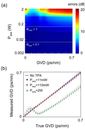
ISCUSSIONSWe numerically investigate the GVD monitoring accuracy
in the presence of TPA and free carriers while varying input
power
. As discussed in Section III, the contribution of
TPA and free-carrier-related effects to the new frequencies
gen-eration around the CW probe becomes significant with high
input power. This directly distorts the RF spectrum captured via
Fig. 5. (a) Numerical results showing the GVD monitoring errors due to TPA-and TPA-induced free carriers compared to pure Kerr nonlinearity while varying input powers. (b) Example of a comparison between (solid line) true GVD and (dots) captured GVD with different input power.
our chip-based radio frequency system automation approach,
hence providing inaccurate GVD monitoring. Fig. 5(a)
illus-trates the GVD measurement errors due to TPA and
free-car-rier effects compared to pure Kerr nonlinearity. The monitoring
errors are defined as
, where
is optical power of new frequencies generated between the
CW probe and fundamental tone at 640 GHz with the subscripts
Kerr and Kerr TPA FC indicating simulations with the Kerr
effect only and with Kerr effect, TPA, and
free-carrier-asso-ciated effects, respectively. We observe that with an average
power
mW, the measurement errors are
insignifi-cant due to the relatively small free-carrier-induced cross-chirp
on the probe compared to Kerr-based XPM. The result confirms
the high measurement accuracy of our silicon-chip-based
moni-toring approach if the upper limit of the operating power for the
condition of
is satisfied.
Fig. 5(b) illustrates the changing accuracy of the GVD
monitoring with varied signal average power inside our silicon
waveguide. Here, we compared the measured GVD to the
true GVD values with different input powers to investigate
the measurement errors owing to TPA and free-carrier effects.
First, the S-shape GVD monitoring curve [see Fig. 4(c)] is
simulated without TPA and free-carrier effects as reference
values. The simulation is then repeated in the presence of TPA
and free carriers. The optical power between the CW probe and
an optical clock tone is captured and compared with the
refer-ence GVD monitoring curve for determining the GVD value
within the system. At low input power (i.e.,
and
110 mW), a good agreement between measured GVD and true
GVD values is demonstrated with a measurement error of less
than 3%. However, the measurement error becomes significant
with higher input power (
W). These numerical results
agree well with our surmise that free-carrier effects will distort
our measurements. The error bars in Fig. 5(b) are calculated
with an assumption that the power meter has 0.5 dB power
fluctuation.
We should note that this silicon-chip-based GVD monitoring
method also works well for nonreturn-to-zero DPSK format
[22]. In this paper, we only show GVD monitoring for 640
Gbit/s RZ-DPSK because we would like to highlight the
broad-band operation capability and high measurement accuracy
(dis-tortions of the RF spectrum of a SUT due to free-carrier-induced
cross-chirp on the probe is negligible) of this approach.
The measurement dynamic range of our chip-based
moni-toring approach is relatively low compared to the results from
[40] while similar input powers were used in both experiments.
This is because the
product of our silicon nanowire is
9
times lower than that of the 2 km highly nonlinear fiber (HNLF)
used in [40], thus resulting in significant less nonlinear phase
shift in the propagation. On the other hand, the high dispersion
of a HNLF introduces large walk-off between an SUT
and a CW probe, yielding much narrower monitoring bandwidth
of
200 GHz (numerical result), without considering the
disper-sion fluctuation along the fiber, compared to 1.6 THz bandwidth
[28] of our monitoring scheme.
VI. C
ONCLUSIONWe have experimentally demonstrated instantaneous GVD
monitoring for ultrahigh bandwidth 640 Gbit/s DPSK signals
based on XPM in a silicon chip. Our investigation shows that
nonlinear losses due to TPA and TPA-induced free carriers do
not affect our monitoring performance. The numerical studies
also provided the operating power limit for our
silicon-chip-based OPM. This scheme is a compact and potentially
cost-ef-fective OPM approach with terahertz monitoring bandwidth,
re-quiring only a CMOS-compatible SOI waveguide, an optical
BPF, and a relatively slow power meter, all of which can be
in-tegrated on a chip.
R
EFERENCES[1] J. Leuthold, C. Koos, and W. Freude, “Nonlinear silicon photonics,” Nature Photon., vol. 4, pp. 535–544, Jul. 2010.
[2] W. Astar, J. B. Driscoll, X. Liu, J. I. Dadap, W. M. J. Green, Y. A. Vlasov, G. M. Carter, and R. M. Osgood, “Conversion of 10 Gb/s NRZ-OOK to RZ-OOK utilizing XPM in a Si nanowire,” Opt. Exp., vol. 17, no. 15, pp. 12987–12999, Jul. 2009.
[3] Ö. Boyraz, P. Koonath, V. Raghunathan, and B. Jalali, “All optical switching and continuum generation in silicon waveguides,” Opt. Exp., vol. 12, no. 17, pp. 4094–4102, Aug. 2004.
[4] Y. Okawachi, M. A. Foster, X. Chen, A. C. Turner-Foster, R. Salem, M. Lipson, C. Xu, and A. L. Gaeta, “Large tunable delays using parametric mixing and phase conjugation in Si nanowaveguides,” Opt. Exp., vol. 16, no. 14, pp. 10349–10357, Jun. 2008.
[5] Y. Dai, X. Chen, Y. Okawachi, A. C. Turner-Foster, M. A. Foster, M. Lipson, A. L. Gaeta, and C. Xu, “1 s tunable delay using parametric mixing and optical phase conjugation in Si waveguides,” Opt. Exp., vol. 17, no. 9, pp. 7004–7010, Apr. 2009.
[6] H. Ji, H. Hu, M. Galili, L. K. Oxenløwe, M. Pu, K. Yvind, J. M. Hvam, and P. Jeppesen, “Optical waveform sampling and error-free demulti-plexing of 1.28 Tbit/s serial data in a silicon nanowire,” presented at the presented at the Opt. Fiber Commun. Conf., San Diego, CA, 2010, Paper PDPC7 (Postdeadline Paper).
[7] H. Ji, M. Galili, H. Hu, M. Pu, L. K. Oxenløwe, K. Yvind, J. M. Hvam, and P. Jeppesen, “1.28-Tb/s demultiplexing of an OTDM DPSK data signal using a silicon waveguide,” IEEE Photon. Technol. Lett., vol. 22, no. 23, pp. 1762–1764, Dec. 2010.
[8] M. A. Foster, R. Salem, D. F. Geraghty, A. C. Turner-Foster, M. Lipson, and A. L. Gaeta, “Silicon-chip-based ultrafast optical oscilloscope,” Nature, vol. 456, no. 7218, pp. 81–84, Nov. 2008.
[9] Q. Lin, J. Zhang, P. M. Fauchet, and G. P. Agrawal, “Ultrabroadband parametric generation and wavelength conversion in silicon waveg-uides,” Opt. Exp., vol. 14, no. 11, pp. 4786–4799, May 2006. [10] J. B. Driscoll, W. B. Astar, X. B. Liu, J. I. Dadap, W. M. J. Green, Y.
A. Vlasov, G. M. Carter, and J. R. M. Osgood, “All-optical wavelength conversion of 10 Gb/s RZ-OOK data in a silicon nanowire via cross-phase modulation: Experiment and theoretical investigation,” IEEE J. Sel. Topics Quantum Electron., vol. 16, no. 5, pp. 1448–1459, Sep./Oct. 2010.
[11] O. Boyraz and B. Jalali, “Demonstration of a silicon Raman laser,” Opt. Exp., vol. 12, no. 21, pp. 5269–5273, Oct. 2004.
[12] H. Rong, S. Xu, O. Cohen, O. Raday, M. Lee, V. Sih, and M. Paniccia, “A cascaded silicon Raman laser,” Nature Photon., vol. 2, pp. 170–174, Mar. 2008.
[13] M. A. Foster, A. C. Turner, J. E. Sharping, B. S. Schmidt, M. Lipson, and A. L. Gaeta, “Broad-band optical parametric gain on a silicon pho-tonic chip,” Nature, vol. 441, pp. 960–963, Jun. 2006.
[14] T. K. Liang and H. K. Tsang, “Efficient Raman amplification in sil-icon-on-insulator waveguides,” Appl. Phys. Lett., vol. 85, no. 16, pp. 3343–3345, Oct. 2004.
[15] B. Corcoran, C. Monat, M. Pelusi, C. Grillet, T. P. White, L. O’Faolain, T. F. Krauss, B. J. Eggleton, and D. J. Moss, “Optical signal processing on a silicon chip at 640 Gb/s using slow-light,” Opt. Exp., vol. 18, no. 8, pp. 7770–7781, Mar. 2010.
[16] G. P. Agrawal, Nonlinear Fiber Optics, 3rd ed. San Francisco, CA: Academic, 2001.
[17] M. Pelusi, F. Luan, T. D. Vo, M. R. E. Lamont, S. J. Madden, D. A. Bulla, D. Y. Choi, B. Luther-Davies, and B. J. Eggleton, “Pho-tonic-chip-based radio-frequency spectrum analyser with terahertz bandwidth,” Nature Photon., vol. 3, no. 3, pp. 139–143, Feb. 2009. [18] T. D. Vo, H. Hu, M. Galili, E. Palushani, J. Xu, L. K. Oxenløwe, S.
J. Madden, D.-Y. Choi, D. A. P. Bulla, M. D. Pelusi, J. Schröder, B. Luther-Davies, and B. J. Eggleton, “Photonic chip based transmitter optimization and receiver demultiplexing of a 1.28 Tbit/s OTDM signal,” Opt. Exp., vol. 18, no. 16, pp. 17252–17261, Jul. 2010. [19] T. D. Vo, J. Schröder, B. Corcoran, J. Van Erps, S. J. Madden,
D.-Y. Choi, D. A. P. Bulla, B. Luther-Davies, M. D. Pelusi, and B. J. Eggleton, “Photonic chip based ultra-fast waveform analysis and optical performance monitoring,” IEEE J. Sel. Topics Quantum Electron., 2011, to be published.
[20] T. D. Vo, M. D. Pelusi, J. Schröder, B. Corcoran, and B. J. Eggleton, “Multi-impairment monitoring at 320 Gb/s based on cross phase mod-ulation radio-frequency spectrum analyzer,” IEEE Photon. Technol. Lett., vol. 22, no. 6, pp. 428–430, Mar. 2010.
[21] T. D. Vo, M. D. Pelusi, J. Schröder, F. Luan, S. J. Madden, D.-Y. Choi, D. A. P. Bulla, B. Luther-Davies, and B. J. Eggleton, “Simultaneous multi-impairment monitoring of 640 Gb/s signals using photonic chip based RF spectrum analyzer,” Opt. Exp., vol. 18, no. 4, pp. 3938–3945, Feb. 2010.
[22] T. D. Vo, J. Schröder, M. D. Pelusi, S. J. Madden, D.-Y. Choi, D. A. P. Bulla, B. Luther-Davies, and B. J. Eggleton, “Photonic chip-based simultaneous multi-impairment monitoring for phase-modulated op-tical signals,” J. Lightw. Technol., vol. 28, no. 21, pp. 3176–3183, Nov. 2010.
[23] R. Claps, V. Raghunathan, D. Dimitropoulos, and B. Jalali, “Influ-ence of nonlinear absorption on Raman amplification in silicon waveg-uides,” Opt. Exp., vol. 12, no. 12, pp. 2774–2780, Jun. 2004. [24] I.-W. Hsieh, X. Chen, J. I. Dadap, N. C. Panoiu, and R. M. Osgood,
“Ultrafast-pulse self-phase modulation and third-order dispersion in Si photonic wire-waveguides,” Opt. Exp., vol. 14, no. 25, pp. 12380–12387, Dec. 2006.
[25] E. Dulkeith, Y. A. Vlasov, X. Chen, N. C. Panoiu, and R. M. Os-good, “Self-phase-modulation in submicron silicon-on-insulator pho-tonic wires,” Opt. Exp., vol. 14, no. 12, pp. 5524–5534, May 2006. [26] Q. Lin, O. J. Painter, and G. P. Agrawal, “Nonlinear optical phenomena
in silicon waveguides: Modeling and applications,” Opt. Exp., vol. 15, no. 25, pp. 16604–16644, Nov. 2007.
[27] M. A. Foster, A. C. Turner, M. Lipson, and A. L. Gaeta, “Nonlinear optics in photonic nanowires,” Opt. Exp., vol. 16, no. 2, pp. 1300–1320, Jan. 2008.
[28] B. Corcoran, T. D. Vo, M. D. Pelusi, C. Monat, D.-X. Xu, A. Dens-more, R. Ma, S. Janz, D. J. Moss, and B. J. Eggleton, “Silicon nanowire based radio-frequency spectrum analyser,” Opt. Exp., vol. 18, no. 19, pp. 20190–20200, Sep. 2010.
[29] C. Dorrer and D. N. Maywar, “RF spectrum analysis of optical signals using nonlinear optics,” J. Lightw. Technol., vol. 22, no. 1, pp. 266–274, Jan. 2004.
[30] H.-S. Hsieh, K.-M. Feng, and M.-C. M. Lee, “Study of cross-phase modulation and free-carrier dispersion in silicon photonic wires for Mamyshev signal regenerators,” Opt. Exp., vol. 18, no. 9, pp. 9613–9621, Apr. 2010.
[31] I.-W. Hsieh, X. Chen, J. I. Dadap, N. C. Panoiu, and R. M. Osgood, “Cross-phase modulation-induced spectral and temporal effects on co-propagating femtosecond pulses in silicon photonic wires,” Opt. Exp., vol. 15, no. 3, pp. 1135–1146, Jan. 2007.
[32] R. A. Soref and B. R. Bennett, “Electrooptical effects in silicon,” IEEE J. Quantum Electron., vol. QE-23, no. 1, pp. 123–129, Jan. 1987. [33] I. D. Rukhlenko, M. Premaratne, and G. P. Agrawal, “Nonlinear silicon
photonics: Analytical tools,” IEEE J. Sel. Topics Quantum Electron., vol. 16, no. 1, pp. 200–215, Jan./Feb. 2010.
[34] S. Afshar V. and T. M. Monro, “A full vectorial model for pulse prop-agation in emerging waveguides with subwavelength structures part I: Kerr nonlinearity,” Opt. Exp., vol. 17, no. 4, pp. 2298–2318, Feb. 2009. [35] X. Chen, N. C. Panoiu, and R. M. Osgood, “Theory of Raman-mediated pulsed amplification in silicon-wire waveguides,” IEEE J. Quantum Electron., vol. 42, no. 2, pp. 160–170, Feb. 2006.
[36] B. A. Daniel and G. P. Agrawal, “Vectorial nonlinear propagation in silicon nanowire waveguides: Polarization effects,” J. Opt. Soc. Amer. B, vol. 27, no. 5, pp. 956–965, May 2010.
[37] R. L. Espinola, J. I. Dadap, R. M. Osgood, S. J. McNab, and Y. A. Vlasov, “Raman amplification in ultrasmall silicon-on-insulator wire waveguides,” Opt. Exp., vol. 12, no. 16, pp. 3713–3718, Jul. 2004. [38] D. Dimitropoulos, R. Jhaveri, R. Claps, J. C. S. Woo, and B. Jalali,
“Lifetime of photogenerated carriers in silicon-on-insulator rib waveg-uides,” Appl. Phys. Lett., vol. 86, no. 7, pp. 071115-1–071115-3, Feb. 2005.
[39] M. A. F. Roelens, S. Frisken, J. A. Bolger, D. Abakoumov, G. Baxter, S. Poole, and B. J. Eggleton, “Dispersion trimming in a reconfigurable wavelength selective switch,” J. Lightw. Technol., vol. 26, no. 1, pp. 73–78, Jan. 2008.
[40] J.-Y. Yang, L. Zhang, X. Wu, O. F. Yilmaz, B. Zhang, and A. E. Willner, “All-optical chromatic dispersion monitoring for phase-modulated sig-nals utilizing cross-phase modulation in a highly nonlinear fiber,” IEEE Photon. Technol. Lett., vol. 20, no. 19, pp. 1642–1644, Oct. 2008.
Trung D. Vo received the B.Eng. (Hons. 1) degree in electrical and computer
systems from Monash University, Melbourne, Vic., Australia, in 2007. He is currently working toward the Ph.D. degree at the Centre for Ultrahigh-Band-width Devices for Optical Systems, Institute for Photonics and Optical Sciences, School of Physics, University of Sydney, Sydney, N.S.W., Australia.
His research interests include high-speed optical communication systems, nonlinear optics, advanced waveguide devices for all-optical signal processing, optical performance monitoring, and all-optical logic functions. He is the author or coauthor of more than 45 papers published in various journals and confer-ences, and holds one patent.
Mr. Vo is a Student Member of the Optical Society of America.
Bill Corcoran (M’08) received the degrees in electronic engineering and
ap-plied physics from RMIT University, Melbourne, Vic., Australia, in 2006, and the Ph.D. degree in physics from the Centre for Ultrahigh-Bandwidth Devices for Optical Systems, University of Sydney, Sydney, N.S.W., Australia, focused on “slow light enhancement of nonlinear effects in silicon nanowaveguides” in 2010.
He is currently a Postdoctoral Fellow at the Chalmers Univeristy of Tech-nology, Gothenburg, Sweden.
Dr. Corcoran became a Student Member of the IEEE Lasers and Electro-Optics Society in 2008. He is a past President of the OSA student chapter at the University of Sydney.
Jochen Schröder received the Diploma degree in physics from the Westfälische
Wilhelms Universität Münster, Münster, Germany, in 2004 and the Ph.D. degree from the University of Auckland, Auckland, New Zealand, in 2009.
In 2009, he joined the Centre for Ultrahigh-bandwidth Devices for Optical Systems, Institute for Photonics and Optical Sciences, School of Physics, University of Sydney, Sydney, N.S.W., Australia as a Postdoctoral Research Associate.
Dr. Schröder is a member of the Optical Society of America and the Aus-tralian Optical Society.
Mark D. Pelusi received the B.Eng. (Hons. 1) degree in electrical and the Ph.D.
degree in electrical engineering from the University of Melbourne, Melbourne, Vic., Australia, in 1994 and 1998, respectively.
From 1997 to 2001, he was a Research Fellow at the Femtosecond Tech-nology Research Association, Tsukuba, Japan, investigating ultra-fast optical communications. He then joined Corvis Corporation, MD, (2001–2003) as a Senior Hardware Engineer, involved in research and development of next gener-ation optical communicgener-ation systems. He is currently a Senior Research Fellow in the Centre for Ultrahigh-Bandwidth Devices for Optical Systems, Institute for Photonics and Optical Sciences, School of Physics, University of Sydney, Sydney, N.S.W., Australia, performing research in nonlinear optical signal pro-cessing and high-speed optical communications.
Dan-Xia Xu is a Senior Research Officer with the IMS-NRC, and also an ad-junct professor with the Department of Electronics, Carleton University.
She joined NRC in 1991 and her work has encompassed high speed SiGe HBTs, silicides for sub-micron VLSI, SiGe and silicide photodetectors, and in-tegrated optics. In 2001-2002 she was part of the research team at Optenia Inc. that successfully developed the first glass waveguide echelle grating demulti-plexer. Her current research interests are in silicon photonics, particularly in ring resonators and other nanophotonic devices for biological sensing and op-tical communications, as well as polarisation management of SOI components. She has authored over 200 scientific publications, including several book chap-ters, and holds 5 patents.
Adam Densmore, biography not available at the time of publication.
Rubin Ma received the M.Sc. degree in electrical and computer engineering
from the University of Alberta, Edmonton, AB, Canada, in 2005.
He is currently a Research Council Officer in the Nanofabrication group at the Institute for Microstructural Sciences of National Research Council Canada, Ottawa, ON, Canada, where he is working in a Silicon Photonics Project. He has expertise in the areas of semiconductor fabrication and packaging.
Siegfried Janz, biography not available at the time of publication.
David J. Moss (S’83–M’88–SM’09) received the B.Sc. degree in physics from
the University of Waterloo, Waterloo, ON, Canada, in 1981, and the M.Sc. and Ph.D. degrees in nonlinear optics from the University of Toronto, Toronto, ON, Canada, in 1983 and 1988, respectively.
From 1988 to 1992, he was a Researcher at the National Research Council of Canada at the Institute for Microstructural Sciences in Ottawa, where he was involved in the research on III–V optoelectronic devices. From 1992 to 1994, he was a Senior Visiting Scientist at the Hitachi Central Research Laborato-ries, Tokyo, Japan, where he was engaged in the research on high-speed III–V modulators and detectors for 10 Gb/s systems, as well as fundamental studies of quantum well tunneling. From 1994 to 1998, he was a Senior Research Fellow at the Optical Fiber Technology Center, University of Sydney, Australia, engaged mainly in the area of silica planar waveguide devices. From 1998 to 2002, he was a Manager and Senior Scientist with JDS Uniphase, Ottawa, Canada, developing products in a number of areas such as fiber Bragg gratings and tunable dispersion compensation devices. He led a team of engineers and scientists that developed a highly successful commercial prototype for tunable dispersion compensation for 10 Gb/s and 40 Gb/s transmission systems. Since 2003, he has been with the University of Sydney, Sydney, N.S.W., Australia, and is currently an Associate Professor at the Centre for Ultrahigh-Bandwidth Devices for Optical Systems working on all optical signal processing, integrated nonlinear photonic circuits and photonic crystal devices. He is also an Adjunct Professor at the Institut National de la Recherche Scientifique, Universite du Quebec, Montreal, QC, Canada. He is the author or coauthor of more than 330 journal and conference papers and three book chapters. He has chaired or participated in many con-ference committees including Optical Fiber Communications (2007–2009), the Lasers and Electro-Optic Society Annual Meeting (2005 to 2009), and Confer-ence for Lasers and Electro-Optics (2005–2007) and has acted as the General Program Chair of the Australian Optical Fibre Technology Conference, Mel-bourne, Vic., Australia, December 2010.
Dr. Moss is a Senior Member of the IEEE Photonics Society and a Fellow of the Optical Society of America.
Benjamin J. Eggleton received the Bachelor’s degree (Hons.) in science and
the Ph.D. degree in physics from the University of Sydney, Sydney, N.S.W., Australia, in 1992 and 1996, respectively.
In 1996, he joined Bell Laboratories, Lucent Technologies as a Postdoctoral Member of Staff, and was then transferred to the Department of Optical Fiber Research. In 2000, he was promoted to Research Director within the Specialty Fiber Business Division of Bell Laboratories, where he was engaged in forward-looking research supporting Lucent Technologies business in optical fiber de-vices. He is currently an ARC Federation Fellow and Professor of physics at the University of Sydney, where he is also the Director of the ARC Centre for Ultrahigh-Bandwidth Devices for Optical Systems, and the Director of the In-stitute of Photonics and Optical Science. He is the author or coauthor of more than 290 journal publications and numerous conference papers.
Prof. Eggleton is a Fellow of the Optical Society of America, the IEEE Pho-tonics Society, and the Australian Academy of Technological Sciences and En-gineering. He was the President of the Australian Optical Society (2008–2010) and is the Editor for Optics Communications. He was the recipient of the 2010 Scopus Young Researcher of the Year Award in the Physical Sciences category, the 2008 NSW Office of Scientific and Medical Research Physicist of the Year Medal, the Pawsey Medal from the Australian Academy of Science, the Mal-colm McIntosh Prize for Physical Scientist of the Year at the 2004 Prime Min-isters Prize for Science, the 2003 International Commission on Optics Prize, the 1998 Adolph Lomb Medal from the Optical Society of America, the Distin-guished Lecturer Award from the IEEE/Lasers and Electro-Optics Society, and the R&D 100 Award.