HAL Id: tel-00195918
https://tel.archives-ouvertes.fr/tel-00195918
Submitted on 11 Dec 2007HAL is a multi-disciplinary open access archive for the deposit and dissemination of sci-entific research documents, whether they are pub-lished or not. The documents may come from teaching and research institutions in France or abroad, or from public or private research centers.
L’archive ouverte pluridisciplinaire HAL, est destinée au dépôt et à la diffusion de documents scientifiques de niveau recherche, publiés ou non, émanant des établissements d’enseignement et de recherche français ou étrangers, des laboratoires publics ou privés.
QUANTIFICATION DE LA CHARGE
MACROSCOPIQUE DANS LES NANOSTRUCTURES
METALLIQUES
P. Lafarge
To cite this version:
P. Lafarge. QUANTIFICATION DE LA CHARGE MACROSCOPIQUE DANS LES NANOSTRUCTURES METALLIQUES. Superconductivity [condmat.suprcon]. Université Pierre et Marie Curie -Paris VI, 1993. English. �tel-00195918�
THESE DE DOCTORAT DE L'UNIVERSITE PARIS 6
Specialite :Physique des solides
presentee par
Philippe LAFARGE
pour obtenir Ie grade de
DOCTEUR de )'UNIVERSITE PARIS 6
Sujet de Ia these:
MACROSCOPIC CHARGE QUANTIZATION
IN METALLIC NANOSTRUCTURES
Soutenue Ie 30 novembre 1993 devant Ie jury compose de MM:
M.DEVORET H. GRABERT P. MARTINOLI 1.E. MOOU B. PANNETIER J.-F. PETROFF
REMERCIEMENTS
Je tiens a remercier tout particulierement Michel Devoret, Daniel Esteve et Cristian Urbina. Au sein du groupe "Quantronique", ils ont su creer une ambiance de travail unique, ala fois amicale et stimulante, et j'ai pu y trouver les conditions ideales pour un travail de these.
J'exprime mes profonds remerciements a Pief Orfila non seulement pour sa contribution technique multiforme a toutes les etapes des experiences mais aussi pour sa disponibilite permanente et son soutien amical.
Ma reconnaissance va egalement
a
Philippe Joyez, mon compagnon de these pendant un peu plus de deux ans. Durant notre travail en commun, j'ai apprecie sa collaboration sans faille qui fut aussi agreable qu'efficace. Je remercie aussi Hugues Pothier avec qui j'ai partage rna premiere annee de these et qui m'a initie aux secrets de l'electronique a un electron, Emmanuel Turlot qui m'a fait decouvrir Ie laboratoire et Edwin Williams pour sa collaboration lors de la premiere experience de boitea
electrons.Pour de nombreuses et fructueuses discussions, je desire remercier Vincent Bouchiat, Andrew Cleland, Thorsten Holst, Antoine Filipe, Morvan Salez et Denis Vion. A plusieurs occasions, j'ai beneficie des connaissances et des conseils avises de Hermann Grabert, John Martinis et Hans Mooij, qu'ils en soient ici remercies.
Je remercie Daniel Beysens de m'avoir permis d'effectuer ce travail de these dans Ie Service de Physique de l'Etat Condense.
Je remercie Hermann Grabert, Piero Martinoli, Hans Mooij, Bernard Pannetier et Jean-Fran<.;ois Petroff d'avoir accepte de faire partie du jury.
TABLE OF CONTENTS
1. INTRODUCTION 1
2.REVIEWOF THEORETICAL PREDICTIONS ON MACROSCOPIC CHARGE
QUANTIZATION IN THE SINGLE ELECTRON BOX 13
2.1 The nonnal electron box 13
2.1.1 The Coulomb staircase and the Coulomb sawtooth at T=0 13 2.1.2 Macroscopic charge quantization at finite temperature 17 2.1.3 Quantum fluctuations of the island charge 21 2.1.4 Tunneling rate in the electron box 27
2.2 The normaVsuperconducting electron box 34
2.2.1 Odd-even symmetry breaking and 2e-quantizationinthe
normaVsuperconducting electron box at T=0 35
2.2.2 Effect of finite temperature 38
2.2.3 Calculation of the odd-even free energy difference D(T,H) 40
2.2.4 Influence of the magnetic field 42
2.2.5 Observability of the 2e-quantization of the macroscopic charge .47
2.3 The superconducting electron box 48
2.3.1 Josephson coupling between the charge states of the box .48 2.3.2 Effect of the electromagnetic environment 52
3. EXPERIMENTAL RESULTS ON THE ELECTRON BOX 59
3.1 Normal case 59
3.1.1 Paper 1: direct observation of macroscopic charge quantization 59
3.2 Superconducting case 77
3.2.1 Paper 2: measurement of the even-odd free energy difference of an
isolated superconductor 77
3.2.2 Paper 3: 2e-quantization of the charge on a superconductor 89
4. CHARGE TRANSFER ACCURACy 101
4.1 Theoretical Predictions 101
4.1.1 Paper 4: passing electrons one by one: is a 10-8 accuracy achievable?.. 101 4.1.2 Paper 5: nondivergent calculation of unwanted high-order tunneling
4.2 Experimental results 141 4.2.1 Paper 6: Direct observation of macroscopic charge quantization:
a Millikan experiment in a submicron solid state device 141
5. CONCLUSION 151
APPENDIX 1: total energy of a general tunnel junctions circuit. 155 APPENDIX 2: fabrication of the superconducting/normal tunnel junctions 163
1. INTRODUCTION
The aim of this work is to demonstrate experimentally the quantization of the charge on a metallic electrode connected to an electron reservoir by a tunnel junction and to show that this phenomenon can be used to transfer electrons one by one from one electrode to another with metrological accuracy.
From the famous Millikan's experiment performed in 1911 [1], we know that the electrical charge on an isolated body is quantized. To demonstrate charge quantization, Millikan used small charged oil droplets. The principle of the experiment was to measure the speed of a single droplet in a gravitational field combined with a variable vertical electrical field. These measurements give access to the mass and the charge of the oil droplet. Millikan showed that this charge is an integer multiple of an elementary electrical charge,
e
==1.6 10-19 C. In his experiment, the charge carried by the oil droplets resulted from the irradiation witha
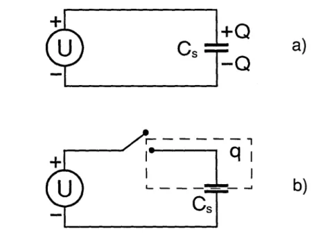
particles produced by a Radium source. Although the charge deposited on the droplet was quantized, it was not controlled. Is it possible to transpose such an experiment in a solid state device and, moreover, to control the stored charge with an externally applied voltage?Surprisingly, the discreteness of the charge carriers does not appear in the usual behavior of electronic circuits. One may think the reason is that any electronic signal involves too large a number of electrons but there is in fact a more profond reason: the conduction electrons are delocalized and form a quantum fluid. To illustrate this effect, let us consider the simple circuit consisted of a capacitor Cs to which we apply a voltage U by perfect leads (see Fig. 1.1a). The charge
Q
stored on the capacitor is equal to CsU and can be precisely adjusted to any arbitrarily small value by varying the applied voltage. Although a charge is transferred from the source to the surface of the capacitor plate, this quantity is a continuous variable. It corresponds to the collective displacement of the charge carriers in the metal with respect to the ionic background. Hence, the charge on the capacitor is not constrained to be an integer number of electrons. The charge quantization can only appearifthe circuit includes an isolated piece of metal. This can be done by opening a switch placed between the voltage source andthe capacitor (see Fig. 1.1 b). One of the capacitor plates is then disconnected from the circuit and forms an isolated electrode. Like the oil droplet of the Millikan's experiment, this electrode contains a well defined number of electrons and its total chargeqis equal to an integer multiple of the electron charge
-e.
As soon as one wants to change this charge, a difficulty arises. Since there is no possibility to transfer electrons from the source to the isolated electrode, the chargeq remains constant and cannot be tuned subsequently with the applied voltage U. Obviously, we can connect the switch again to modify q, but simultaneously, we will suppress the quantization of the electrode charge.
+Q
-Q
a)
. - - - ,
I~ql
I
-L
I
l... - - - ~b)
C
sFig. 1.1 a) Capacitor connected to a voltage source. The charge Q=CsU on the capacitor plate is not quantized. b)If one opens a switch between the voltage source and the capacitor, the portion of the circuit inside the dashed line box contains a charge q which is quantized butfixed.
How can we combine charge quantization and charge transfer? We certainly need a more elaborate device than a usual switch. A highly resistive tunnel junctions provides a way to maintain both the quantization of the electrode charge and the possibility to vary it.
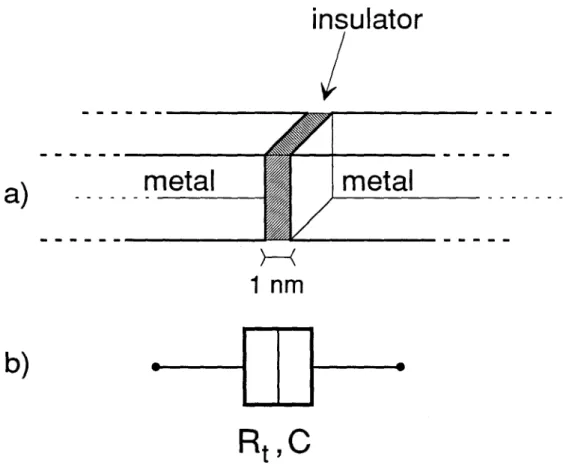
A tunnel junction consists of two metallic electrodes separated by a thin insulating layer (see Fig. 1.2). In such a device, the mechanism of conduction is the tunnel effect of electrons
through the insulating barrier. A tunnel junction is characterised by two parameters, its capacitance C and its tunnel resistance Rt •This latter quantity is determined experimentally by the current I
=
V/ Rt which flows through the device when a voltage V is imposed to thejunction. The tunnel resistance is a phenomenological macroscopic parameter which depends on the area and the thickness of the insulating layer. Although it has the dimension of a resistance, Rt does not correspond to any dissipative process like the resistance value in a usual resistor. The tunnel resistance can be expressed through the relation
R
t-1
=
(2e
2Ih)NJ,
where N is the number of conduction channels and
J
is the transmission coefficient of the barrier for each channel, assumed to be independent of the channel index.Elaborate theoretical considerations [2,3] show thatifthe junction tunnel resistance Rt is much larger than the resistance quantum RK
=
hie
2==25.8 kQ, electrons are localised on either side of the insulating barrier and electron tunneling through the barrier is a stochastic Poisson process with a rate given, at zero temperature, byfilll
Rte
2, where fill is the energydifference before and after the tunnel event. Thus, provided Rt
»
RK , the charge of anisolated electrode connected to an external electron reservoir by such a tunnel junction will remain quantized. Apart from its tunneling properties, the junction behaves like a capacitor with a capacitanceC.
Let us replace, inthe simple circuit of Fig. 1.1 b, the switch by a tunnel junction with a tunnel resistance such that Rt » RK •Therefore, we maintain the quantization of the charge of
the isolated electrode but the transfer of electrons from the voltage source is now allowed by tunnel events across the junction. We have called "electron box" [4] this basic circuit consisting of a tunnel junction and a capacitor placedin series with a voltage source (see Fig. 1.3). Since the electrons can enter and leave the electrode formed between the junction and the capacitor, this electrode is isolated in the sense that it is surrounded everywhere by insulating material. We call "island" this particular kind of electrode for which the instantaneous charge only varies by tunnel events and remains quantized in units ofe.
Although the instantaneous number nof excess electrons on the island is quantized, the average number
(n)
may vary smoothly with the gate voltage U. The really observable quantity is the macroscopic charge of the island(-ne).
Ifwe want(n)
itself to be quantized, we mustmetal
J=
-insulator
/
;,..+
-" ' - - - -
--
- ---
-
-
-
--metal
--
---
---
--a)
>---<
1
nm
b)
•
OJ
•
Rt,C
Fig 1.2 a)A tunnel junction consists of two metallic electrodes separated by a thin insulating layer. b) In circuit schematics, a tunnel junction is represented by a double box symbol and characterized by its tunnel resistance Rt and its capacitanceC.
---,
C
I
-ne
I
I
I
_ _ _ _ _ _ 1
Fig. 1.3 Circuit diagram of the electron box which consists of a tunnel junction and a capacitor placed in series with a voltage source. The metallic electrode between the junction and the capacitor forms an "island" which contains a well defined number of excess electrons.
suppress the thermal fluctuations of the island charge. The characteristic energy of the charge quantization phenomenon is the charging energy Ec=
e
2/2(
C+
Cs ) equal to the energy cost of putting one excess electron in the island when there is no voltage applied. Charge quantization requires that the charging energy Ec is much larger than the characteristic energy kBT of the thermal fluctuations where kB is the Boltzmann constant. The condition Ec » kBT ensures that the thermal fluctuations of the island charge are negligible. A circuit temperature of about T "'"30 mK is attainable with a dilution refrigerator. This implies that the island capacitanceCisland=C
+
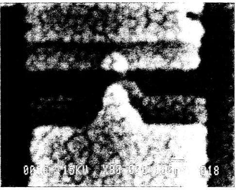
Cs must be lower than 1fF to satisfy the latter inequality. Such low capacitanceis achieved by using tunnel junctions with a typical area of 100 nm x 100 nm. We have fabricated this type of nanoscale junctions using a combination of electron beam lithography and shadow evaporation through a suspended mask [5]. The junctions are located at the overlap between two metallic thin films. A scanning electron microscope photograph of such a junction is shown on Fig. 1.4. The bottom metallic electrode is made of aluminum, the insulating layer is obtained by oxidizing the surface of the aluminum layer, and the top electrode is made either of aluminum or copper alloyed with 3 % of aluminum in weight. We have thus fabricated two different types of nanostructures: Al/AIOx/AI or Al/AIOx/Cu. To measure the charge increment of the island, we have used a single-electron transistor [6] as an electrometer. This device is fabricated together with the box and is capacitively coupled to the island of the box. The coupling capacitance Cc is sufficiently small not to affect the behavior of the single-electron box and we assume that the temporal average charge Ii measured by the electrometer is equal to the thermal ensemble average(n).
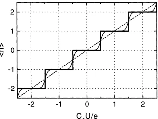
When plotted versus the gate voltage U, the average number
(n)
of excess electrons in the island takes the form of a staircase: the "Coulomb staircase" depicted on Fig. 1.5. The number of electrons adjusts itself to minimize the total energy of the circuit given byE=Ec(n-Cs
Uje)2.
At T =0, the staircase steps are perfectly flat and each one correspondsto a fixed number of electrons inside the island. At high temperature (kBT» Ec )' one finds
(n)
=CsU, the island macroscopic charge quantization is suppressed and the junction acts as a short circuit. Note that the instantaneous charge of the island is still quantized; only the average charge takes non integer values. At lower temperature (Ec «kBT), the staircase isFig. 1.4 Scanning electron microscope photograph of an aluminum/aluminum-oxide/copper tunnel junction.
just slightly rounded (see Fig. 1.5) and the central part of the steps corresponds to a well defined number of electrons inside the island. The voltage required to inject one electron in the island is equal to the period of the staircase given by
e/C
s ' This latter quantity is in the mV range for the gate capacitance Cs of the order of 100 aF. Hence, provided Ec«kBT, one can precisely control the number of electrons inside the island with a macroscopic voltage. We have called this effect "macroscopic charge quantization" because the island charge is distributed over a macroscopic number of atoms. It is important to note that unlike the usual charge quantization of an isolated piece of matter, the macroscopic charge quantization defined above is only exactinthe limitT ~0, Rt /RK ~00. While the former limit corresponds to thesuppression of thermal fluctuations, the latter limit corresponds to the suppression of the quantum fluctuations due to the tunnel process itself [3].
If we consider now a single-electron box with an island made of superconducting material, the previous analysis must be modified since electrons are pairedina superconductor. Ifwe assume that the island is a perfect superconductor following the BCS theory [7], all the electrons are paired and the energy cost of an unpaired electron is at least equal to the superconducting energy gap ~ [8]. For ~>Ec and at low temperature, electrons should be transferred two by two from the electron reservoir into the superconducting island by creating or suppressing Cooper pairs in the island. As we have shown, the superconducting electron box indeed exhibits a 2e-quantization of the island charge [9]. In this regime, the height and the length of the staircase steps are twice as large asinthe non-superconducting case, as shownin Fig. 1.6. However, if the charging energy Ec is sufficiently large with respect to ~, Cooper pairs can be broken and electrons enter the island one by one [10]. In that case, we observe that the staircase is asymmetric with long steps corresponding to the states with an even number of electrons inside the island and short steps corresponding to an odd number of electrons (see Fig. 1.6). This odd-even asymmetry [10,11,12] will persist when the temperature is increased until the odd-even free energy difference D(T) vanishes. This quantity D(T) depends strongly on the temperature through the relation D(T)'"
~-kBTlnNeff+O(T2)
[11] where Neff is the effective number of states available for excitations in the island. From the staircase asymmetry we can measure the odd-even free energy difference [10]. In this regime,A
e
V ~ ~ ~ ~ ~;;:;
2
~""":""""""""";""""""""";""""""""";'''''''''f ;;:
i ; I I I I , , ' I I I I" I I • I I . , , ' o;J;
.
; ;1 - --.
~-.
~-
~. -. - If ;;
0 - • - • ~ - • - -• , I " I • I ; ' I.
..-: o;j;
I I I " I ,o -
~:
"I/""';~;"'o~"-' ~ ~ -II,' I ;.
.
l.
I.
o I.
I I , I • ... i .. - - i - - i - - - - i --.
.
; ; o;;:J
l
'
I .", • , • _ __ • - • r • - • - ,.,.~"""'..6".-..
r • • • - • - • • • r - • • • - • - • - r • - •-If
" 1 I ; ;.
.
; I ; ; ;-2
;: /
J
~/I
-2
-1
1
2
Fig. 1.5 a) Theoretical variations of the average number (n) of excess electrons in the island of the electron box as afunction of the reduced charge CsUje when T=0 (solid line), when
kBTjEe =0.1 (thin line), and in the limit kBT» Ee (dashed line).
2.0
0.5
1.0
1.5
CsU/e-QO
.
I I.
I~I
T= 25.6 mK
I
r
I- -~-
J -(--
-~ J -I I I2.0 0.0
0.5
1.0
1.5
CsU/e-QO
0.0
0.0
2.0
I
T= 201 mK
I
-
01.5
0
-'e
I-
Q)1.0
... ::) (/J ()0.5
-'e
Fig. 1.5 b)Solid lines: experimental variations of the average number Ii of excess electrons in in the island of an electron box. Dashed lines: theoretical calculations for an island capacitance C};,
=
0.8 fF. The experimental parameters of the circuit are Cs=
74 aF and·
1
.
,
- ~ .. I .. .. ·I... -· . I ~ I f , . . . . . . .• _ • I I I ~.. - : - .. co - : - _1 ~ -: -I I I I I ... r 1 "'I -I I • I t I I t ~.. "'," ,'" ,'" i 1- ~ "', -, -I I I I I ' I I I I I I I3
~ I ' ' ~ ~ .! - to , -I I I I • I I I I I I I ,2
1
o
A Cv
I-2
I - ...- - - - -...'r '~ . . . L • • - • - • ! • • • • - • J • • • • - • •' • • • I I • I I I I I I I I ,3
I I I l I I _ ~__ <IIf/I ,'" '" ra r " , _ I I I I I I I-3
-2
-1
0
1
2
3
CsU/e
Fig. 1.6 a) Theoretical variations of (n) as a function ofCsU/e for a superconducting island at zero temperature. Inside the 2e-quantization regime (11
>
Ee ), the height and the length of the steps are twice as large as in the non-superconducting case (solid line). When 11<
Ee, the incremental charge is equal to e (dashed line, calculation done for 11/Ee =0.4).6
-
--
...
-.-..
oa
"-"Ie
I.-..
~
::>
tJ) () "-"Ie
2
o
-2
-4
_ .. _ _ _ __.
_ _ ~- .J.l . . . L ... L . . . L . . . L. . . .L . . . L•. - _. . . ._~ ,.
... :...
~---....-_pt/'..
.
... __ · · .. __ · _·,.· _,.· .. · · r .. C' , . _ _ , . . .-1
o
1
2
3
CsU/e-Qo
Fig. 1.6 b) Experimental variations of the average number
n
of excess electrons in a superconducting island at T=
40 mK when 11=
0 (top), when I1/Ee=
0.83 (middle), and when I1/Ee =1.22 (bottom). For the sake of clarity, the two lowest curves have been shiftedthe island charge quantization provides an energy scale
E
c with whichD(T)
can be directly compared. A similar effect arises ifone depresses the superconducting gap ~ by applying a magnetic field to the sample.Fmally, the electron box, which consists of one island, can be seen as the basic element of more complex circuits which include several islands. In the charge transferring devices [13,14] such as the "turnstile" [15] or the "electron pump" [16], gate voltages are used to transfer electrons from an island to another in order to build a current electron by electron which circulates in an external current-measuring apparatus. The electron pump circuit, for example, can be described as two electron "boxes" connnected through a third junction. For this device, there is a two-dimensional stability diagram analogous to the Coulomb staircase of the single-electron box [16]. As a current source, the electron pump is a potential candidate for a current standard. However, higher order tunneling processes [17-22] can directly transfer a single charge across two or more tunnel junctions although single electron tunneling across each junction is forbidden. These processes, usually referred to as cotunneling processes, reduce the accuracy of the electron pump and must be take into account to evaluate the metrological applications of such a device [23-25].
In this work, we present experiments based on nanoscale tunnel junctions, which both demonstrate that the macroscopic charge, i.e. the mean value of the total charge, of a metallic electrode is quantized and that we are able to control this charge at the single-electron level. In chapter 2, we review the theoretical foundations and the limits of the macroscopic charge quantization. We present in chapter 3 experimental results on the electron box, both in the non-superconducting and the non-superconducting state. Chapter 4 is devoted to the accuracy of the charge transferring devices. We report experimental results performed on a four junctions device and calculations of the transfer accuracy of the pump. Appendix 1 presents the calculation of the total electrostatic energy of a general circuit consisting of junctions, capacitances and voltage sources. The fabrication techniques of the superconducting/normal tunnel junctions used in the superconducting electron box are described in appendix 2 and the measurement device, the SET electrometer, is presented in appendix 3.
REFERENCES
[1] R.A. Millikan, Phys. Rev. 32, 349 (1911).
[2] K. A. Matveev, Zh. Eksp. Teor. Fiz. 99, 1598 (1991) [Sov. Phys. JETP 72,892 (1991)]. [3] H. Grabert, Proceedings of the LT20 conference (1993).
[4] P. Lafarge,H.Pothier, E. R. Williams, D. Esteve, C. Urbina, and M. H. Devoret, Z. Phys. B 85, 327 (1991).
[5] G.J. Dolan and J. H. Dunsmuir, PhysicaB152, 7 (1988). [6] T. A. Fulton and G. J. Dolan, Phys. Rev. Lett. 59,109 (1987).
[7] J. Bardeen,L.N. Cooper andJ. R. Schrieffer, Phys. Rev. 108, 1175 (1957). [8] D. V. Averin and Yu. V. Nazarov, Phys. Rev. Lett. 69, 1993 (1992).
[9] P. Lafarge, P. Joyez, D. Esteve, C. Urbina, and M. H. Devoret, Nature 365,422 (1993). [10] P. Lafarge, P. Joyez, D. Esteve, C. Urbina and M. H. Devoret, Phys. Rev. Lett. 70, 994
(1993).
[11]M. T. Tuominen, J. M. Hergenrother, T. S. Tighe and M. Tinkham, Phys. Rev. Lett. 69, 1997 (1992).
[12] T. M. Eiles, J. M. Martinis and M. H. Devoret, Phys. Rev. Lett. 70, 1862 (1993).
[13] D. Esteve, inSingle Charge Tunneling,edited byH. Grabert and M. H. Devoret (plenum, New York, 1992), Chap. 3.
[14] M. H. Devoret, D. Esteve and C. Urbina, Nature 360,547 (1992).
[15] L. J. Geerligs, V. F. Anderegg, P. A. M. Holweg, J. E. Mooij, H. Pothier, D. Esteve, C. Urbina and M. H. Devoret, Phys. Rev. Lett. 64,2691 (1990).
[16]H. Pothier, P. Lafarge, D. Esteve,C. Urbina and M. H. Devoret, Europhys. Lett. 17,249 (1992).
[17] D. V. Averin and A. A. Odintsov, Phys. Lett. A 149,251 (1989). [18] D. V. Averin and Yu. V. Nazarov, Phys. Rev. Lett. 65,2446 (1990).
[19] L. J. Geerligs, D. V. Averin andJ. E. Mooij, Phys. Rev. Lett. 65, 3037 (1990).
[20] D. V. Averin and Yu. V. Nazarov, inSingle Charge Tunneling, edited by H. Grabert and M. H. Devoret (Plenum, New York, 1992), Chap. 6.
[21] T. M. Eiles, G. Zimmerli, H. D. Jensen, and John M. Martinis, Phys. Rev. Lett. 69, 148 (1992).
[22] V.I.Mel'nikov, Phys. Lett. A 176, 267 (1993).
[23] H.D. Jensen and J. M. Martinis, Phys. Rev. B 46, 13407 (1992).
[24] D. V. Averin, A. A. Odintsov and S.V. Vyshenskii, J. Appl. Phys. 73, 1297 (1993).
[25] H. Pothier, P. Lafarge, D. Esteve, C. Urbina and M. H. Devoret, IEEE Trans. Instrum. Meas. 42,324 (1993).
2. Review of Theoretical Predictions on Macroscopic
Charge Quantization in the Single-Electron Box
In this chapter we review the theoretical predictions concerning macroscopic charge quantization of a metallic island. We fIrst treat the case of an electron box consisting only of normal metal elements. We will afterwards treat the case of a box with a superconducting island and a normal metal reservoir. Finally, we will treat the case where both the island and the reservoir are superconducting.
2.1 The normal electron box.
2.1.1 The Coulomb staircase and the Coulomb sawtooth at T=O.
The electron box circuit consists of a small tunnel junction of capacitance C and a capacitor Cs placed in series with a voltage source U (Fig. 2.1). The "island", which is the metallic electrode common to the junction and the capacitor, is free to exchange electrons with the charge reservoir consisting of the "lead", i.e. the electrode common to the junction and the voltage source. Since the lead wave impedance Zt is much less than the resistance quantum
RK =hi
e
2 ==25.8 kQ, the charge q of the island is the sole degree of freedom of the system whose states can be indexed by the number n of excess electrons on the island [1]. For the moment, we assume that the junction tunnel resistance Rt is much larger than the resistance quantum RK • Under this condition, as we will see in Sec. 2.1.3, n is a good quantum number [2,3].At T =0, the charge q=
-ne
is fIxed and determined by the integer numbern
for which the total energy of the circuit is minimal. The total energy of the electron box including the work done by the voltage source is (see appendix 1):(1)
Since we want to compare the energy of the different n-states for a given value of the voltage U,we can retain only the first term of the right hand side of Eq. (1) and defme:
(2) Here, we have introduced the charging energy Ec
=
e2/2Cr., Cr.=
C+
Cs being the totalcapacitance of the island. The quantity Ec is the cost of putting one excess electron on the island when U=O. Expression (2) clearly shows that the minimum of En corresponds to a number n of excess electrons equal to the integer closest to CsUIe. Consequently, at T =0, the equilibrium value of n as a function of CsUIe takes the fonn of a staircase function (Fig. 2.2b) which we have called the Coulomb staircase. We must mention that the expression "Coulomb staircase" is also used [4,5] to denote the steplike structure in the current-voltage characteristic of a double junction circuit. However, there is no conflict since both staircases originate from the same basic effect.
We have plotted in Fig. 2.2a the energies En versus CsUIe for different values of n. They are represented by a set of parabolas, each parabola being shifted from its neighbors by 1 along the
x
axis. The system has in general a non-degenerate ground state, which fixes the equilibrium value of n at T =0, except when the two lowest n-states have the same energy En'This latter situation corresponds to the crossings of parabolas and occurs for the half integer values of the reduced variable CsUIe. At these threshold points, the ground state is degenerate and transitions between the n-state and the
(n
+
I)-state of the box can occur. Such a transition corresponds to a single tunnel event across the junction, transferring one electron in or out the island.The charge Q on the junction capacitance, the charge Qs on the capacitor Cs and the number n of electrons stored in the island are related as follows:
C Q=-(-ne+CsU) Cr. Q = - n e + -Cs C CU s Cr. Cr. s (3)
Let us examine the evolution of these three quantities as we sweep the voltage U (Fig. 2.3). At
U
=
0, the n=
0 state is the ground state and the energy cost of one excess electron is exactly equal to the charging energy Ec ' Then, the energy difference between the n=0 state and theI
+Q
s
I
-Q
s
+Q
-Q
r---t\
t - - - tI
q=-ne
C
s
C
I
IFig. 2.1 Schematic of the single-electron box circuit consisting of a capacitor and a tunnel junction placed in series with a voltage source. The symbol inform of a double box represents the tunnel junction. The part of circuit inside the dashed line is the "island" which contains a number n of excess electrons.
a)
<n>
CsU/e
4
3
b)
2
1
1
2
3
4
CsU/e
Fig. 2.2 a) Energy of the circuit versus CsUIe for several values of the number n of excess electrons in the island. The charging energy Ee is the electrostatic energy of one extra electron in the island when CsUIe=O. The solid dots correspond to level crossings between parabolas where one electron can tunnel into and out the island. b) The Coulomb staircase which displays the equilibrium value of n as a function of CsUIe.
2
1
A
c
0
V-1
-2
Q)-....
A
a
v
I I.
I.
I I -~ -~ -~ -I I I I.
I2
Q)1
-....
A
(/)0
a
v
-1
-2
-2
-1
0
1
2
CsU/e
Fig. 2.3 Average value at T =0 of the number n of excess electrons in the island (top), of the charge Q on the junction (middle) and of the charge Qs on the capacitor (bottom) versus
capacitance grows linearly with U. When CsU
j
e=1/2, the two states n= 0 and the n=1 have the same energy and the transition n=0~n=1 can occur. The charge of the electron entering the island is distributed over the two capacitancesC
and Cs ' Thus, the charge Q on the junction exhibits a negative jump equal to-e(
CjCrJ
while the capacitor charge Qsexhibits a positive jump equal to e(CsICrJ After the transition, the n=1 state becomes the new ground state and Q grows again from a negative value. The variations of the charge Q on the junction as a function of the reduced variable CsUIe are periodic sawtooth oscillations: we call them the Coulomb sawtooth.The three discontinuous curves depicted in Fig. 2.3 are actually three different manifestations of the same effect: the steplike variations of the equilibrium number of excess electrons on the island. The charge increment is fixed by the charge quantum
e
and the periodicity of the phenomenon is set by ejCs .2.1.2 Macroscopic charge quantization at finite temperature.
According to the previous electrostatic calculation, the charge q on the island of the electron box at T =0 is fixed when CsUIe¢ 1/2 mod 1 and the steps of the resulting Coulomb
staircase are thus perfectly flat. The question now arises of the robustness of the steps to thermal fluctuations of the island charge. At finite temperature, the system can be found in excited states corresponding to the various n-states of the box. The quantity of interest is the thermal average
(q)
=-(n)e,
hereafter referred to as the "macroscopic" charge of the island.Using expressions (2) and (3), the charge
Q
on the junction can be expressed as:(4)
At finite temperature, this relation is transposed to average values. The average junction charge
(Q)
and the free energyF are related by:C aF
(Q)=cau'
s
(5)
where F=-kBTIn Z. Here T is the temperature of the system, kB is the Boltzmann constant and Z is the partition function of the system given by:
n=+""
Z =
"Lexp(-EnlkBT).
n=-oo
(6)
Combining Eq. (3) and Eq. (5), we can express the thermal average number
(n)
of excess electrons in the island as:(7)
This expression is particularly useful at high temperatures. For large values of the reduced parameter
e=
kBTlEe'
the series (6) does not converge numerically and one computes the partition functionZusing the following identity[6]:When
e»
1, we can keep only the fIrst term of the sum in the right hand side of Eq. (8). In this limit, using Eq. (7) the average(n)
is thus approximately given by:(9)
At low temperature, we have to go back to the defInition of
(n).
We calculate directly the Boltzmann average of the number n of excess electrons. Each n state is weighted by its Boltzmann factor exp(-EnlkBT)
and the average(n)
is given by:n=+""
"Lnexp(- EnlkBT)
(n)
=.;.;;.n;_;:_;"" _"L
exp(-EnlkBT)
n=-oo (to)When
e«
1, a useful approximation is obtained by keeping in Eq. (10) only the two terms corresponding to the lowest energies. Within this approximation, ifwe consider CsUIe
in the neighborhood ofm
+
1/2,
one readily shows that(n)
takes the form:(n)
=
m
+.!.{
1+
tanh[-(m
+
1/2-CsUle)/e]) .
The two quantities
(n)
and(Q)
are plotted versusCsU je
in Fig. 2.4 for three different values of the reduced parameter 8. A quantitative measurement of the effect of temperature on the Coulomb staircase is its slope at the half integer values ofCsU je:
for 8« 1
a(n)
(CUje=m+l/2)
=_1a(csUje)
s
28
=1
+
4n
28e-
81t2 for 8» 1.(12)
These two expressions give the same value of the slope for 8 "" 0.34216. Finally, in the limit
T~0, we recover the perfect Coulomb staircase since Eq. (7) reduces to:
(13)
where EG refers to the ground state energy.
At high temperature, Eq. (9) shows that the quantization of the macroscopic charge
(q)
=-(n)e
is completely suppressed. Although the instantaneous chargeq
remains always quantized, the mean value(q)
becomes equal to-CsU
in the limit kBT»E
c ' In that case, the tunnel junction behaves as a short circuit and its average charge(Q)
is zero. The macroscopic charge quantization occurs in the opposite limit:(14) This condition ensures that the Coulomb staircase is just slightly rounded by thermal fluctuations and that in the central part of the steps the mean value
(n)
remains equal to an integer number (Fig. 2.4a).Like the Coulomb staircase, the Coulomb sawtooth is also rounded at T:I: 0 and the amplitude of the oscillations is less than
(CjCrJe
(Fig 2.4b). The Coulomb sawtooth is similar but not identical to the single electron tunneling (SET) oscillations which are expected to occur for a small tunnel junction biased with a perfect current source [7]. In that latter effect, the voltage across the junction oscillates between+elC
and-ejC
at frequencyf
=lie,
whereI
is the current applied to the junction. However, the Coulomb sawtooth arises from the macroscopic charge quantization and is an equilibrium effect while the SET oscillations involve a dynamic blockade of tunneling.2
1
"
c
0
V-1
-2
Q)---
"
0
a
v
I.
I I.
I.
I'"
,.
"
I I-"
,8=0.02
I,,.
"
"'"
--- 8=0.1
'"
'"
'"
I8=0.5
"
I - - - -...
,,-
,"
-I"
I ' "...
"',
"
I"
,-
,-,
"
I I'"
'"
..-.'"
I"
I I"'" ,, ,."
.. ' J-"
I"
I'"
'"
a)
'"
I"
I...
, " -, I"
I ' " I I I I I r,.
.
-2
-1
0
1
2
CsU/e
Fig. 2.4 a) Average value (n) of the number of excess electrons in the island and b) average charge
(Q)
on the junction versus CsUIe for three different values of the reduced parameter8=kBTlEe' Note that when 8=0.5 (dashed lines) the Coulomb staircase has been reduced
to an almost linear ramp while the modulation of the average junction charge
(Q)
is still visible.Experimentally, a sample can be reliably cooled down to about 30 mK. It means that the island capacitance C:E must be in the tF range to satisfy condition (14). This is achieved using ultrasmall tunnel junctions with typical area of 100 nmx100 nm fabricated by nanofabrication techniques. Since the capacitance Cs can be made smaller than 1 tF, the period
e/Csof the Coulomb sawtooth will be a voltage (> 1 mY) sufficiently large to be easily controlled. The experimental observation of the Coulomb sawtooth and its temperature dependence are described in the next chapter (see section 3.1.1).
In summary, provided an adequate tunnel junction is used, the number of electrons
stored in the island does not fluctuate at low temperature and is entirely determined by the externally applied voltage. The Coulomb staircase reveals the macroscopic charge quantization arising from the electrostatic energy gap between the different n states of the island. At finite temperature the aspect of the staircase depends on two external parameters: the capacitance Cs and the charging energy Ec 'The former one determines the length of the steps of the staircase, the latter one determines the sharpness of the charge jumps.
2.1.3 Quantum fluctuations of the island charge.
We now discuss the case where the transmission coefficient of the insulating barrier of the junction is finite. The finite tunnel conductance of the junction, which has been neglected so far, makes the island charge subject to quantum fluctuations. Even at T =0, the ground state is not a pure n state and we expect the charge of the island not to be strictly quantized. We shall now discuss the correction to the staircase dependence of the island charge on U and treat the tunnel hamiltonian as a perturbation.
Quantum mechanically, the single electron box is described by the following hamiltonian:
H= Ho+Ht , (15)
where H
o
describes the system in the absence of tunneling and Ht is the perturbing tunnel hamiltonian. The unperturbed hamiltonian Ho
is given byH
o
=
Ec(ri - CgUler
+
LEk
Lat
Lak
L+
LEkRatRakR '
kL kR
where
Ii
is the operator associated with n the number of excess electrons stored in the island, akL and akR are the quasiparticle annihilation operator in the island and in the lead respectively,
Ek
L and EkR being the kinetic energies of the quasiparticles measured from the Fermi energy.
Note that in Eq. (16) the ak's are purely kinetic degrees of freedom while
Ii
is the sole electrical degree of freedom. In the limit of large electrodes,Ii
and the ak's are independent. In the one-dimensional model of the tunnel junction, the tunnel hamiltonian [8] Ht is written:(17)
where t is the matrix element which characterises the tunneling across the junction and
[8,
Ii]
=i. In Eq. (17) we have assumed that the tunnel matrix element t is independent of the energy of the ingoing and outgoing quasiparticle. One can show that the tunnel resistance Rt of the junction and the tunnel matrix elementt are related by(18)
where PLand PR are the density of states at the Fermi level on each side of the junction. Since
the pattern of the Coulomb staircase is periodic in CsU
Ie,
we will restrict our calculation to the range -1/2<CsUIe
<1/2, inside which the unperturbed ground state is given byn
=O.At the lowest order in Hp the n=0 state is coupled to the states n=1 and n=-1. The
corresponding corrections CEil to the ground state energy take the form
(19)
where E±1 refers to the total electrostatic energy of the n=±1 state defined by Eq. (2). Using (18) and making a change of variable E
=
EL+
ER'we get:(20)
Inserting this result in Eq. (13), we obtain the average number of excess electrons [9] in the island:
(21)
where g
=
RK / 4rc2Rt •This expression diverges atCsUIe
=
±1f2.Grabert [2] has calculated the correction to
(n)
up to second order in g and has obtained:(22)
where
(23)
Here S.t.
(-x)
refers to the same sum of terms withx
replaced-x,
and Li2=Jo
dz
In(l-z)/z.
For Rt =O.5RK , Grabert shows that the second order calculation is sufficient to describe the variations of
(n)
in 98% of the interval -1f2<CsUIe
<+
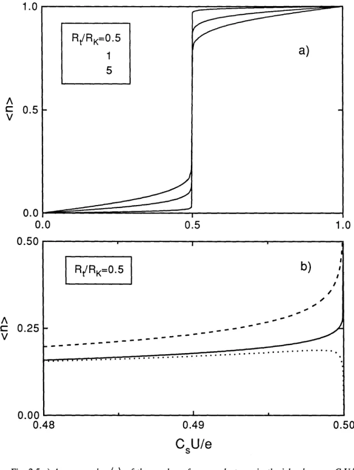
1f2 (see Fig. 2.5b). At the threshold values CsUIe
=
±1f2, the second order expression (22) diverges logarithmically like (21). In order to remove the divergence, Matveev [3] has used an analogy with the Kondo problem and has re-summed the most diverging logarithmic terms. Grabert has done a systematic diagrammatic expansion and has obtained after re-summation for CsUI
e
~1/2:-g*In 8*
(n)
=*
*
+
O(8) ,
1-2g In8 (24)
where the renormalized parameters g* and 8* are given by g* =g[1+6g+0(g2)],
8*
=
8[1-ag +O(g2 )], 8=
1f2 - CsUIe,
and a=
-9.7726....This calculation predicts that the island charge is not strictly quantized and varies approximately linearly with the voltage U in the center of the flat part of the staircase. Fig. 2.5 shows the two effects of a finite tunneling conductance on the Coulomb staircase: a [mite slope in the middle of the steps and a weak rounding as CsU
Ie
~±1f2. However, the slope at CsUI
e
=± 1f2 remains infinite like in theR
tIRK
~00 limit. We must mention that, using a1.0
R/R
K=0.5
1
a)
5
Ac
0.5
v
1.0
0.5
0.0
l--~~::::::=:::;;:::=~~---J
0.0
0.50
r---~·----~I---....,...---ab)
,
,
I I / ; "....
-A
-~
0.25·
__ ---
~
~---...
'.0.50
0.00 ...
---.---.-..1---...-.---...
0.48
0.49
CsU/e
Fig. 2.5 a) Average value (n) of the number of excess electrons in the island versus CsUJe calculated using Eq. (22) and Eq. (24) for three different values of the ratio RtlRK' b)
Enlargement of the preceeding curve in the vicinity of CsUJe=0.5 for RtJRK= 0.5. The solid line is the non divergent result, the dashed line is the first order calculation given by Eq.
1.0
1---7~~;;;;=---_,~
oJ(A
c:
0.5
~V
-~
0.0
.-I0.0
0.5
1.0
CsU/e
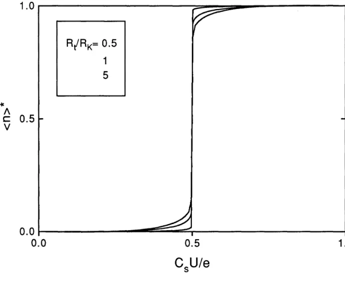
Fig. 2.6Renormalized average number (n)
*
of excess electrons in the island as a function ofdifferent approach, Zwerger [10] has predicted a finite slope of the staircase at CsU
Ie
=±lj2, in contradiction with the preceeding analysis.A word of caution is necessary at this point. Because we cannot perform an absolute measurement of the island charge, the curves plotted in Fig. 2.5 cannot be directly compared with experimental results. The experiments are only sensitive to the relative variations of
(n).
In Fig. 2.6, we have plotted the staircase calculated with (22) and (24) in a "canonical form", i.e. with flat steps and normalized charge increment. This canbe done by substracting the steps slope and rescaling of the curve. We obtain for the renormalized average charge
(n)
*:
(n)*
=(n)-4g(C
sUje) .
1-4g
(25)The curves plotted in Fig. 2.6 show that, even for tunneling resistances of the order of RK , the charge quantization is experimentally a good approximation and that the charge jumps are always well defined. Nevertheless, the effective incremental charge is always smaller than the charge quantum. The reduction factor equal to (l-
4g)
can reach 10 % forR
t "'"R
K . If we assume that quantum and thermal fluctuations can be treated separately, the charging energy which can be extracted from the staircase at finite temperature is only a renormalized quantityE;
given by:(26)
Finally, we must mention that Biittiker et al. [11] have considered the quantum corrections to the capacitance of a mesoscopic capacitor. They emphasize the fact that one cannot describe a mesoscopic capacitor simply with its geometrical capacitance but that the experimentally relevant capacitance is an electrochemical capacitance. This distinction is valid onlyifthe density of states of the capacitor plates are small compared to
cel
e
2, where Ce
denotes the geometrical capacitance. However, for the typical dimensions of the metallic islands used in electron box experiments, this condition is not satisfied and we can neglect the corrections to the geometrical capacitances.
2.1.4 Tunneling rate in the electron box.
In this section, we will calculate the tunneling rate across the junction of the electron box, taking into account the effect of the electromagnetic environment [8,12].
Inthis approach, we include in the description of the circuit the impedance Z(0)) which models the electromagnetic environment of the electron box and which is placedin series with the junction (see Fig. 2.7 a). The impedance Z (0)) takes into account the fmite resistance of the bias circuitry as well as radiation losses in the lead. The junction itself is represented by a pure tunnel elementin parallel with a capacitance C. The equivalent circuit seen by the pure tunnel element is an effective voltage sourceVeff in series with an impedance Zt(0)) (Fig 2.7b). The
effect of the environment on the tunneling rate is contained in the real part of the total impedance Zt(0) ).
The total impedance Zt(0)) can be described as a capacitance C~ =C
+
Cs in serieswith an impedance K2Zc(0)) [13], where K
=
Cs/C~
and Zc(O))=
Z(0))[1+
jKCroZ(0))r1(Fig 2.7c).Ifthe low frequency behavior of the impedance Z(0)) corresponds to that of a resistanceR,then limro.-.+OZc (0))=limro.-.+OZ(0))=R.Denoting the junction temperature byT, the rate
r
of a tunneling event across the junction is [8,12]
r=_1_[00
E P(!1E-E)dE,Rt
e
2-00
l-exp[-E/kBT] (27)where Rt is the tunnel resistance of the junction, M is the difference between the total energy of the circuit before and after the tunneling event, and the function P(E) is the probability that the tunneling electron creates an excitation of the electromagnetic environment with energy E. The function
p(
E)
is a functional of the real part ofZt(0)).Ifp electrons have already passed through the junction and if limro.-.+OZ (0))=R, the
energy difference M associated with a tunneling event which increasespis
e
2M=KeU-(p+l/2)- .
C~ The function P(E) is given [8] by
1
1+
00 P(E)=- exp[J(t)+iEt/1i]dt, 21th - 0 0 (28) (29)Z(oo)
a)
b)
c)
Fig. 2.7 a) Schematic of the single-electron box circuit coupled to its electromagnetic
environment. The junction is represented by a pure capacitor of capacitance C in parallel
with a pure tunnel element of resistance Rt symbolized by a double T. The electromagnetic
environment of the circuit is modeled by an impedance Z(
ro)
in series with the voltagesource. b) The circuit seen by the pure tunnel element is the total impedance
Zt
(ro)
in serieswith an effective voltage source Vet!. c) The total impedance
Zt(ro)
can be described as awhere
i
OOdro Re[
Zt (
ro)] ( (1 )
. )
J(t)=2
-
coth 2~hro(cosrot-1)-isffirot .
o ro RK
(30)
In this expression ~= 1/
kBT
e , whereT
e is the temperature of the environment which can be different from the temperature of the junction T involved in Eq. (27). Under common experimental conditions, the real part of the environmental impedance Re[Zt
(ro)] is small compared with the resistance quantum RK , particularlyin the electron box. This can be seen from Re[Z/(ro)] =1(2Re[Zc(ro)]. Typically 1(<0.1, hence we can evaluate the functionP(E)
by making a linear expansion of
exp[J(t)]
in Eq. (29). At zero-th order inRe[Zt(ro)]/R
K ,P(E)
reduces to a delta function3(E)
and the rater
is simply given byr-
1 !::£- R/e
2 1-exp[-!::£/kBT] .
(31)Eq. (31) constitutes the so-called "global" rule formula of the tunneling rate [14]. The limit
P(E)
=3(E)
corresponds to an electron box completely decoupled from its electromagnetic environment.We now develop
exp[J(t)]
to fIrst orderinRe[Zt(ro)]/R
K . The functionP(E)
can be expanded as1 f.+oo
P(E)
~-
(1
+J(t))exp[iE t/n]dt .
21th - 0 0
Rewriting Eq. (30) as
J(t)
= 2f.+00 dro Re[Zt(ro)]e-
irot -1 , ro R 1-e-
131iro - 0 0 K we obtain P(E)=3(E)[1-2f.+OOdror(ro) 1]+2r(E/n)
1 , - 0 0 ro 1-e
-13hro E 1-e
-13E (32) (33) (34)where r(ro) =
Re[Zt(ro)]/R
K . The fIrst order expansion made in Eq. (32) is equivalent to considering that a tunnel event can create or annihilate only one energy quantum in one of the oscillators modelling the environment [12].If E>0 (E<0), the function
pee)
given by Eq. (34) can thus be interpreted as the probability for the environment to emit (absorb) one quantum of energy E (-E). Introducing the Bose factorn(
0) =1/[
exp(~nro)-1]
and the coupling coefficient c(0) =2r(
0))/nO), one can relate the functionpee)
to the probabilities of emission or absorption of an energy quantum bro. The probability P(nro) to emit one quantum of energy bro by a single tunneling event is given by P(nro)=c(ro)(n(ro)+l). On the other hand, the probability PC-nO)) to absorb one quantum is given by P(-nro)=c(ro)n(ro).We consider finally a general type of environment where the impedance Z( ro) is a 1-port network consisting of several impedances ZI(ro), Z2(0)'"'' Zm(O) at different temperatures
Ii,
T2 , ... , Tm (Fig 2.8a). We denote by aj(ro) the attenuation coefficient of a voltage source placed in the branch of the circuit which contains the iinpedance Z; (0) and measured at the port of the network. From circuit theory, a;(ro) is also the attenuation coefficient of a current source placed at the port of the network and measured in series with the impedance Z; (ro). The theory of networks only consisting of impedances yields the three following relations: 2az
a· = -Iaz.
1 m Z(ro)=
laf(ro)Z;(O) ;=1 m .,Re[Z(ro)]=lla;(ro)l- Re[Z;(O)]
;=1
(35)
(36) The impedance Zc(ro)=Z(ro)/[l +jKCroZ(O)] and the impedances Zci(O) given by Zc;(ro) =Z;(ro)/[l +jKCroZ(ro)] (Fig. 2.8b) obey the same set of relations as Zero) and the impedances Z; (ro). Assuming that each impedance Zci (ro) is at thermodynamic equilibrium at
1';,
we can generalize Eq. (34) topee)
=C(E)[l-1+
00
K2~la'(0)12
2r;(ro) dro ]~ I 0) 1- -13;hro
- 0 0 1=1 e
+K2Ila;(E/fl)1
2
2r;(E/fl) 1_13
,£,
_T_m~
Zm{ro}
1.0.. __' - - - , - - - ,.---tH
](2 a : Z,,(oo)
F-:
](2a~Z,m(oo)
C+C
S :1:
I :1:
I 1 I ' m , 1 - - - - 1 _Fig 2.8 a) Schematic of a single-electron box circuit connected to an environmental impedance Z(oo) consisting of a i-port network of impedances at different temperatures. b)
The impedance Zc(oo) (see Fig. 2.7c) can be represented by m impedances at different temperatures placed in series. The coefficient
aj(OO)
is the attenuation of a current source placed at the port of the network and measured in series with the impedance Zj(00) .
---
I ,---,
,
' T ' ' T
, 11 ' , 12
,---_.
---Fig. 2.9 Example of an environmental impedance Z(oo) consisted of two parts at temperature
At high positive energy (E> 0) the spontaneous emission is the dominant decay process and the effect of the temperatures T1, T2 , ••• , Tp of the environment on the tunneling rate is negligible. In that case, P(E) is well approximated by P(E)::::: l(22Re(Zc(E/Ii)]/ERK •
The situation is very different in the case of absorption processes (E<0) for which the function P(E) and consequently the tunneling rate are strongly affected by the environmental temperatures. In that case, one can regard each impedance Zci
(00)
as a voltage noise source [15] at temperatureT;.
The effect of the impedance Zci(oo) is characterized by a spectrum density of voltage noise Syi(OO) such that P(E) can be expressed as:where
E
Syi(E/Ii) =2/1tRe[Zci(E/Ii)] (
~
).l-exp - iE (38)
When E=-lim<0, the spectrum density of voltage noise SYi(E/Ii) is given by Syi(-(0)=2/1tRe[Zci(m)]ni(m)lioo. Here nj(m) corresponds to the distribution of photons in the impedance Zj
(00)
at temperatureT;.
More generally, we can define a spectral density Sy(m) for the whole environment given by Sy(oo)
=
I;!ai(oo)12Syi(m). Since the spectral density Sy(oo) is a sum involving different temperatures it cannot be described by a constant equivalent noise temperature. Finally combining Eq.(27) and Eq. (37) we obtain1 M, [
i+
oo
2 1tSy(E/Ii)(I1E-E l_e-AElkBT ) ]
r
=- - 2 -AElk T 1+
J( 2 -(AE-E)/k T-1 de . (39)Rte 1-e B - 0 0 E I1E 1-e B
As an example, we consider the circuit depicted in Fig. 2.9. The environmental impedance Z( m) is separated in two parts at temperatures
Ii
and T2 and is given by Z(oo)=alR1+a~R2+a~R3 with a1=1, a2=R3/(R2+R3) and a3=R2/(R2+R3). In the center of a step at CsUIe
=0, the ground state of the box corresponds ton
=0 and the energy difference with the first excited statesn
=
1andn
=
-1 is equal to -Ec ' A log-log plot of theE/h
(0[Hz]
T
1=T
2=40 mK
I
~
10-
2110-
2210-
2310-
24,...,
N10-
25I
C\I-->
...
10-
26-
8
10-
27--
>en
10-
2810-
2910-
3010
7Fig 2.10 Spectral density of the voltage noise as a function of the frequency calculated for the
circuit of Fig. 2.9, in the case where R1
=
49 Q, R2=
100 Q, R3=
1Q and Cr. =C+
Cs =1fF .function Sv (-(0) is shown schematically in Fig. 2.10 when RI
=
49 .Q, R2=
100 .Q, R3=
1.Q, and C:r=
1if for two casesIi
=
T2=
40 mK and TI=
40mK« T2=
4 K. WhenIi
«T2 ,the dominant noise at frequency
me
=
Ee/n comes from the resistor R2 at T2 • Thisoff-equilibrium tunneling rate calculation shows how crucial low temperature filtering is to prevent the activation of tunnel events from parts of the measuring circuit at higher temperatures.
2. 2 The normal/superconducting electron box.
Inthis section, we consider the case of a superconducting electron box where the island is made of a superconducting metal and connected to a non-superconducting lead through a superconducting/normal tunnel junction. We can regard the island as a small piece of superconductor free to exchange charges with an electron reservoir. According to the BCS theory of superconductivity, electrons are paired in the ground state of a superconductor [16]. The pairing of electrons clearly breaks the invariance of the ground state with respect to the parity of the total numberN of conduction electrons. Since, in the island of the electron box, this numberN is fIxed, we must distinguish two cases depending on the parity ofN. If N is even,all the electrons can be paired in the island and there is a unique superconducting ground state. If N is odd, one electron should remain unpaired as a quasiparticule excitation with an energy at least equal to the BCS energy gap .1 and the superconducting ground state is degenerate. As pointed out by Averin and Nazarov [17], this odd-even asymmetry should result in a parity dependence of the ground state energy of the box. We will discuss in this section how the electron box experiment can reveal this odd-even asymmetry. We will also show under which conditions the macroscopic charge on a superconductor is quantized in units of2e.
2. 2. 1 Odd-even symmetry breaking and 2e-quantization in the normal/superconducting electron box at T=0.
For the sake of simplicity, we fIrst assume that the total number N of conduction electrons in the island and the number
n
of excess electrons have the same parity. At T=0 and in absence of magnetic fIeld, the total energyEof the superconducting box is given by(40)
where Do is the energy difference at T=0 between the odd-n and the even-n ground states of the system, and Pn =nmod 2. The first term in the right-hand side of Eq. (40) is the usual total electrostatic energy En of the circuit of the non-superconducting case, hereafter referred to as the normal case. The second term is a parity dependent energy which corresponds to the fact that an unpaired electron must remain when the number of electrons stored inthe island is odd. IfNand nhave opposite parities, Pnis given by Pn =(n+l)mod2.
The BCS theory predicts that in zero fIeld the excitation energy Do is equal to /1, the superconducting energy gap of the island. Nevertheless, a fInite magnetic fIeld or the presence of paramagnetic impurities inside the sample can induce pair-breaking effects [18]. As we shall see in section 2.2.4, these effects modify the quasiparticles energy spectrum of a superconductor. Thus the excitation energy Do involvedin the ground state energy of the box is not necessarily equal to the pair potential/1in the superconducting island.
In Fig. 2.11, we plot the energy Eversus CsU
Ie
and we get a set of parabolas indexedby n. The odd-n parabolas are shifted up with respect to the even-n parabolas by an amount
equal to Do.Therefore, atT
=
0, the energy cost of adding one extra electron inthe islandwill depend crucially on the relative magnitude of the charging energy Ec and the excitation energy gap Do.Two cases must be distinguished:i) When Do <Ec (Fig. 2.11 b), the incremental charge of the Coulomb staircase is still equal to ebut the even-n steps are longer than the odd-n steps. The experimental observation of such an asymmetric staircase is reported in Sec. 3.2.1. In comparison with the normal case, when Uincreases, it is now more "diffIcult" for the system to attain an odd-n state but "easier" to leave it. If
n
is even, the energy cost of the addition of one electron in the island is the suma)
GsU/e
<n>
5
4
3
b)
2
1
1
2
3
4
GsU/e
E
Do
c)
E
c
GsU/e
<n>
4
2
d)
GsU/e
1
2
3
4
Fig 2.11 Energy of the norma/lsuperconducting electron box as a function of CsUIe for several values of the number n of excess electrons in the island when Ec