HAL Id: hal-01917898
https://hal.archives-ouvertes.fr/hal-01917898
Submitted on 8 Jan 2019
HAL is a multi-disciplinary open access
archive for the deposit and dissemination of
sci-entific research documents, whether they are
pub-lished or not. The documents may come from
teaching and research institutions in France or
abroad, or from public or private research centers.
L’archive ouverte pluridisciplinaire HAL, est
destinée au dépôt et à la diffusion de documents
scientifiques de niveau recherche, publiés ou non,
émanant des établissements d’enseignement et de
recherche français ou étrangers, des laboratoires
publics ou privés.
Annealing-free Si3N4 frequency combs for monolithic
integration with Si photonics
Houssein El Dirani, Ayman Kamel, Marco Casale, Sébastien Kerdiles,
Christelle Monat, Xavier Letartre, Minhao Pu, Leif Katsuo Oxenløwe,
Kresten Yvind, Corrado Sciancalepore
To cite this version:
Houssein El Dirani, Ayman Kamel, Marco Casale, Sébastien Kerdiles, Christelle Monat, et al..
Annealing-free Si3N4 frequency combs for monolithic integration with Si photonics. Applied Physics
Letters, American Institute of Physics, 2018, 113 (8), �10.1063/1.5038795�. �hal-01917898�
1
Annealing-free Si
3N
4frequency combs for monolithic integration
with Si photonics
Houssein El Dirani
1, Ayman Kamel
2, Marco Casale
1, Sébastien Kerdiles
1,
Christelle Monat
3, Xavier Letartre
3, Minhao Pu
2, Leif Katsuo Oxenløwe
2,
Kresten Yvind
2, and Corrado Sciancalepore
11Univ. Grenoble Alpes, CEA-LETI, Minatec, Optics and Photonics Division, 17 rue des Martyrs, F-38054
Grenoble, France
2DTU Fotonik, Technical University of Denmark, Kgs. DK-2800 Lyngby, Denmark 3Institut des nanotechnologies de Lyon, UMR CNRS 5270, Ecole Centrale Lyon, F-69130, Ecully, France
Silicon-nitride-on-insulator (SiNOI) is an attractive platform for optical frequency comb generation in the telecommunication band because of the low two-photon absorption and free carrier induced nonlinear loss when compared with crystalline silicon. However, the high-temperature annealing that has been used so far for demonstrating Si3N4-based frequency combs made the co-integration with silicon-based optoelectronics elusive, thus reducing dramatically its effective complementary metal oxide semiconductor (CMOS) compatibility. We report here on the fabrication and testing of annealing-free SiNOI nonlinear photonic circuits. In particular, we have developed a process to fabricate low-loss, annealing-free, and crack–free Si3N4 740-nm-thick films for Kerr-based nonlinear photonics featuring a full process compatibility with front-end silicon photonics. Experimental evidence shows that micro-resonators using such annealing-free silicon nitride films are capable of generating a frequency comb spanning 1300-2100 nm via optical parametrical oscillation based on four-wave mixing. This work constitutes a decisive step toward time-stable power-efficient Kerr-based broadband sources featuring full process compatibility with Si photonic integrated circuits (Si-PICs) on CMOS-lines.
Kerr optical frequency combs constitute a paradigm shift in the development of high-capacity data transmission, integrated spectroscopy, high precision metrology, and frequency synthesis [1]. Since 2010, silicon-nitride-on-insulator (SiNOI) has imposed as an attractive chip-based platform for the generation of wideband frequency combs pumped at telecom wavelengths, because of its relatively high nonlinearity (×10 that of silica and larger than that of highly nonlinear Hydex glass [2]) as well as the absence of two-photon absorption and free carrier generation that plague crystalline silicon. In the meanwhile, silicon photonic integrated circuits (Si-PICs) have demonstrated increasing maturity levels for a wide range of optical functions such as III-V-on-Si integrated lasers [3], high-speed modulators [4], Ge-on-Si photodiodes [5], as well as filters and wavelength (de)multiplexers [6], thus continuously highlighting the potential of silicon optoelectronics integration with cost-effective complementary metal-oxide-semiconductor (CMOS) technology [7, 8]. In this context, the monolithic integration of Kerr-based frequency combs with Si photonics and CMOS micro-nano-electronic nodes holds the promise for on-chip high-capacity transmitters that would benefit from the maturity and low cost of CMOS manufacturing and scalability.
The realization of relatively thick (> 700 nm) stoichiometric Si3N4 films, as required by microring frequency combs, which
imply both a tight confinement of light and anomalous group velocity dispersion (GVD), remains challenging. In particular,
all prior works strictly made use of long high-temperature annealing (~1200 °C for at least 3 h) of the deposited silicon nitride
film [9-12]. This extreme annealing step has been accounted for by the need to densify the silicon nitride film through driving out excess hydrogen and break N-H bonds, so as to get closer to a stoichiometric Si3N4 film and reduce the material absorption
loss in the C-band. However, this annealing induces thermal stress that eventually leads to cracks during the device processing unless sophisticated pre-patterning strategies are adopted prior to the film deposition [10, 11]. Yet, in the perspective of nonlinear optics-silicon optoelectronics co-integration, these extreme annealing temperatures would severely degrade the front-end-of-the-line (FEOL) silicon optoelectronic circuits underneath. Specifically, doped optical circuits would be unacceptably affected by the undesirable dopant diffusion in junction-based Si modulators and by the hetero-interface degradation of Ge-on-Si photodetectors. As an alternative, optical parametric oscillation has been demonstrated by using the proprietary composition of Hydex waveguides in 2013 [2]. However, the nonlinear parameter 𝜸 of Hydex is six times lower than that of silicon nitride, thus increasing the required power for frequency comb generation, hence the risk of waveguide optical damage. Comb
2
generation has also been demonstrated in 2018 using deuterated silicon nitride (SiN:D) deposited at 300 °C [13]. However, although being a CMOS-compatible processing building block, it is worth to point out that deuterated silicon nitride can be exclusively used during the back-end-of-the-line (BEOL) fabrication, thus preventing a straightforward monolithic integration with both silicon photonics and sub-100 nm standard CMOS electronics circuitries during a collective FEOL processing [14]. Furthermore, this material has a relatively strong thermal shift that occurs from the larger residual hydrogen-related absorption coefficient (when compared to purely stoichiometric Si3N4 films) making it difficult to stabilize the comb in the soliton state as described in [13]. In
addition, for similar resonance quality factors, deuterated silicon nitride microresonators require higher threshold powers for comb generation than stoichiometric Si3N4, which indicates a lower nonlinear index of SiN:D and
increases, as for the Hydex, the risk of waveguide optical damage.
Very recently, we reported a method that avoids thermal annealing for growing relatively thick (740 nm) crack-free Si3N4-based straight nanowaveguides with good linear and nonlinear properties, as measured by self-phase
modulation of picosecond pulses propagating along these waveguides [15].
In this paper we report a comb generated from a microresonator made in an intrinsically CMOS-compatible annealing-free silicon nitride, following a tailored deposition method and without the typical hour-long 1200 °C post-annealing that is detrimental to the integration with front-end silicon optoelectronic circuits. Our annealing-free and crack-free fabrication process (shown in Fig. 1) provides our devices with the right specification (i.e., microring group velocity dispersion and characteristics) to underpin Kerr frequency combs, thus representing a significant step toward the full compatibility of Si3N
4-basedKerr comb sources with the thermal budgets of Si photonics processing. In contrast to all previous approaches, our process does not exceed neither the dopant activation temperature (1030 °C) required for Si modulators [16], nor the H2
annealing thermal budget used for dislocation control of Ge-on-Si photodiodes (825 °C) [17]. Furthermore, our approach would offer a clear advantage even in the perspective of silicon photonics full integration with sub-100 nm standard micro-nano-electronics CMOS circuits during collective FEOL processing [18].
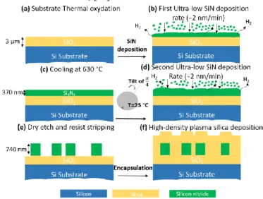
In order to control strain and to prevent cracks from appearing, the silicon nitride layer is deposited on a (non-patterned) substrate via low-pressure chemical vapor deposition (LPCVD) in two steps of 370-nm-thick layer each. The deposition is carried out with a tailored ultra-low deposition rate (< 2 nm/min) to produce a very high quality film, which is denser optically, and highly nonlinear (n2 = 𝟑. 𝟔 𝒙 𝟏𝟎−𝟏𝟓𝐜𝐦𝟐 𝐖−𝟏) [15].
FIG. 1. Schematics of the annealing-free fabrication process for Si3N4 nonlinear photonics (a)-(f).
Critically, under such a low deposition rate which is 40 % lower than that of standard LPCVD silicon nitride reported in [19] and 30 % lower than the deposition rate mentioned in [20], the thermal activation energy enables silicon and nitrogen to dispose at the silicon nitride film surface via atomic surface migration phenomena, while compelling hydrogen to escape the film. Furthermore, between the two deposition stages, the wafer is rotated by 45° in order to distribute the uniaxial strain along the overall film thickness, thus avoiding film cracks upon subsequent subtractive patterning. Each deposition run is carried out at 780 °C with post-deposition cooling to around 630 °C for 20 minutes. Controlled ramp-ups and -downs from/to 780 °C at 10 °C/minute to/from 630 °C are used prior to each deposition which is carried out under a 112 mTorr pressure using NH3 (200 sccm) and SiH2Cl2 (80 sccm) precursor gases, thus providing a ratio between the two precursor gases
(SiH2Cl2:NH3) of 0.4. For comparison, the deposition of silicon-rich silicon nitride requires this ratio to be higher than 2 [21],
which typically implies an increase of the SiH2Cl2 gas flow as well as a decrease of the NH3 gas flow rate. According to [22],
a decrease in the NH3 gas flow inevitably translates into an increase in the deposition rate. Regarding nitride-rich silicon nitride
films, the deposition rate is of the order of 17 nm/min [23], which is much higher than our deposition rate too.
The long thermal annealing step adopted in standard LPCVD processes is used to densify the SiN film, through bringing sufficient energy to break up N-H bonds otherwise causing absorption in the material. By reducing the content of residual
3
hydrogen [11, 19] in the SiN film, the high tensile strain is a clear indication of the film stoichiometry [19, 21]. In order to compare between the stoichiometry of films produced via our annealing-free process and by the standard LPCVD process including a long post-annealing step, we compared their respective tensile strains. The stress of our silicon nitride film is inferred by measuring the wafer bow, before and after removing the silicon nitride from the wafer back side. The material morphological characterization revealed a tensile strain around +1200 MPa, which is 1.5x times higher than the value of 800 MPa reported in [11], employing a long post-annealing step and considered, so far, as the state of the art in stoichiometric silicon nitride processing for nonlinear applications and optical parametric oscillators.
Another indication of the remaining N-H bonds is provided by the spectral dependence of the intrinsic quality factor (𝑄𝑖 ) measured for a Si3N4 micro-ring resonator with 1.4 µm waveguide width (see figure 2). It roughly
increases by a factor 2 while moving away from the N-H overtone absorption peak (near 1520 nm), showing the presence of residual N-H bonds in our film. The losses in the ring can be estimated by the expression [19] 𝛼 =𝑘0𝑛𝑔
𝑄𝑖
where 𝑘0 is the wavenumber and 𝑛𝑔 is the mode group index of the waveguide with similar width. The difference
between the losses at 1550 nm (𝑄𝑖= 350,000) and the losses at 1520 nm (𝑄𝑖= 190,000) can thus be estimated to
be 0.9 dB/cm. This additional loss due to residual N-H absorption for our annealing-free process is comparable to the value (0.6 dB/cm) inferred for high-temperature annealed Si3N4 waveguides [21], and, as shown below, it does not
preclude the oscillation and comb generation in the C-band.
FIG. 2.Intrinsic quality factor as a function of wavelength for an annealing-free silicon nitride microring resonator (waveguide width equal to 1.4 µm). The darker colored line shows the mean value and the brighter shadowed areas illustrates the standard deviation of the measurements.
The Si3N4 circuits were patterned through a combination of deep UV lithography (I-line, 780-nm-thick resist) and
fluoride-based (CF4-CH2F2-O2) dry etching. They were encapsulated by 3-µm-thick SiO2 cladding layer at 400 °C
using high-density plasma-enhanced chemical vapor deposition (HDP-PECVD) to avoid void formation, which is considered to be one of the main causes for device failure. Figure 3(b) shows optical and electron scanning microscope images of the fabricated devices.
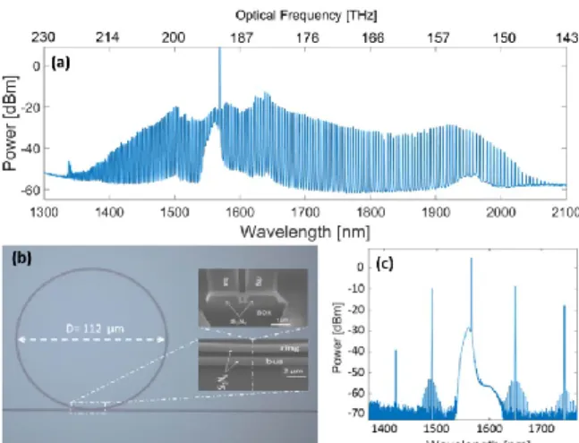
The combination between the four-wave mixing processes within the resonator and the optical parametric oscillation results in Kerr frequency comb generation. The optical spectrum out of an annealing-free silicon-nitride-on-insulator microring with a 56-µm radius is shown in Fig 3(a). The cross-section dimensions (1.5-µm-wide × 740-nm-thick) of the ring waveguide ensure that GVD is anomalous at the 1569 nm pump wavelength. The intrinsic quality factor of the microring – which is separated by a 350 nm gap from the bus waveguide - exceeds 580,000. A relatively smooth native line spacing (~406 GHz) frequency comb spanning across about 800 nm between 1300 nm - 2100 nm is obtained for ~1 W TE-polarized continuous-wave power (Pin) coupled in the bus waveguide. This power value is
comparable to the power required (2 W) to fill the entire comb span using high-temperature annealed Si3N4 rings with
loaded quality factor of 100,000 (intrinsic quality factor 200,000) [2] and to the pump power (3 W) used to generate an optical frequency comb in similar annealed Si3N4 ring resonators [24]. A spectrum recorded for Pin ~300 mW, i.e., well above
the oscillation threshold, is also shown in Fig. 3(c). The comb spacing is wider in this case, as dictated by the spectral gain of degenerate four-wave mixing imposed by the device GVD.
4
FIG. 3. Comb generation using annealing-free silicon nitride on insulator. (a) A 800-nm-spanning comb generation using a 56-µm-radius Si3N4 microresonator for coupled power Pin ~ 1 W. (b) Optical microscope and (insets) scanning electron microscope images of the ring and coupling region. (c) Comb spectrum for Pin ~ 300 mW.
In order to draw a comparison between our annealing-free process and the standard LPCVD process using a long post-annealing, some wafers have been annealed at 1050 °C under N2 atmosphere for 2 hours. This annealing
condition was the most extreme we could apply on our CMOS line. Quite surprisingly, we did not observe a clear and significant improvement in the resonance linewidths. One primary reason might be related to our relatively low annealing temperature value as compared with that used by other groups (typically > 1200 °C) which is very close to the silicon wafer fusion limit [12]. A second explanation might originate from the significant value of the mode scattering loss induced by the substantial microring side-wall roughness. The latter has still room for improvement to well below <1 nm RMS via sophisticated pattering strategies which are currently under investigation. Such large scattering loss contribution to the Q-factor of our microring resonances may thus hide the relatively minor gain in Q factor brought by the 1050 °C annealing step, which likely falls within our Q factor measurement uncertainty. In any case, our work shows that a sufficient amount of hydrogen can be driven out of the Si3N4 film using our deposition
process, so as to get closer to stoichiometric silicon nitride films and to generate a frequency comb.
Regarding the damage threshold of our devices, throughout the whole measurement time (~6 months), we observed only one single waveguide fusion event, out of a total tested device number of ~40, which occurred under continuous-wave coupled power levels above 38 dBm. We think that such fusion event originates from local continuous-waveguide imperfections (such a side-walls scattering or other local defects such as encapsulation voids and impurities) as well as waveguide ageing (notably at the upper cladding Si3N4-SiO2 interface), partly due to the aforementioned residual
N-H absorption tail in the annealing-free SiN films. Again though, this low device failure statistics points out that its impact is rather limited.
In order to measure the threshold power for optical parametric oscillation (OPO), the device was pumped with increasing power levels coupled to the bus waveguide. The laser wavelength was scanned across a resonance at 1570 nm. The chip output light was passed through a short pass filter with a cut-off wavelength of 1560 nm that blocks the pump light with an extinction ratio of 60 dB and was then detected by a photodiode. The peak power of the filtered short wavelength OPO signal at each power coupled to the bus waveguide shows that the measured signal exceeds the noise floor (of -50 dBm) above a threshold power of ~ 83 mW.
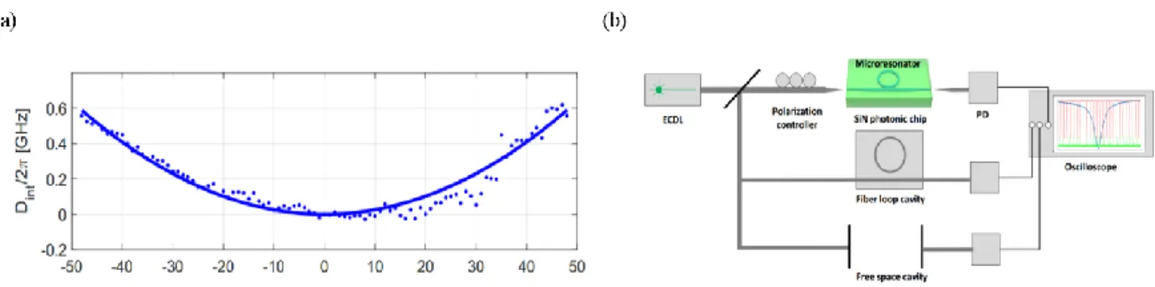
We measured the dispersion of our devices by scanning an ECDL light while recording the device transmission and two calibration traces from a fiber cavity and a high-finesse free space cavity with FSR of 171MHz and 175MHz, respectively. The integrated dispersion of the micro-cavity is 2 2 3 3
int( ) 1
2 6
D DD D where
isthe angular frequency,is the mode number relative to the pumped mode and Diare the dispersion coefficients. Fig.
4(a,b) depict the measured dispersion and the measurement setup. A fit of the measured dispersion gives an anomalous dispersion value of D2 2 511kHzat 1580 nm which is equivalent to a group velocity dispersion of 29
ps/nm/km. This value compares well with our finite element modeling of the dispersion which gave us an anomalous dispersion estimate of 50 ps/nm/km at the same wavelength. Note that the values of simulated and measured dispersion are in agreement with the simulated dispersion of similar annealed Si3N4 waveguides (1.65-µm-wide ×
5
FIG. 4. Dispersion measurement of the TE mode of a ring resonator with 200 µm radius and 1.5 µm width. (a) Plot of the integrated dispersion. (b) Experimental setup used for the dispersion measurement.
In conclusion, these results show that it is possible to generate a wideband comb at telecom wavelengths using annealing-free silicon nitride nonlinear circuits featuring a full FEOL process compatibility with Si photonics. We demonstrated that annealing-free silicon nitride frequency comb microresonators can be made following a tailored deposition method, minimizing the hydrogen content. Our annealing-free and crack-free fabrication process provides our devices with the right specification (microring group velocity dispersion and characteristics) to underpin Kerr frequency combs, thus representing a significant step toward the full compatibility of Si3N4-based
Kerr-comb sources monolithic integration with standard CMOS and Si photonics processing. Through allowing the monolithic integration of broadband comb sources with CMOS-compatible optoelectronics, our work represents a milestone toward the realization of next-generation Petabit/s data transmitters on a chip.
Funding. DOPT 2020 internal funding program (CEA-LETI). Danish Research Council SPOC (DNRF-123) center of
excellence silicon photonics for communications (SPOC) (DTU). ERC H2020 GRAPHICS (648546) and the Institut Universitaire de France (INL).
References
1P. Marin-Palomo, J. N. Kemal, M. Kaprov, A. Kordts, J. Pfeifle, M. H. Pfeiffer, P. Trocha, S. Wolf, V. Brasch, M. H.
Anderson, R. Rosenberger, K. Vijayan, W. Freude, T. J. Kippenberg, and C. Koos, Nature 546, 247(2017).
2D. J. Moss, R. Morandotti, A. L. Gaeta, and M. Lipson, Nat. Photonics 7, 597 (2013).
3B. Ben Bakir, A. Descos, N. Olivier, D. Bordel, P. Grosse, E. Augendre, L. Fulbert, and J.- M. Fedeli Opt. Exp., 19,
10317, (2011).
4L. Liao, D. Samara-Rubio, M. Morse, A. Liu, D. Hodge, D. Rubin, U. Keil, and T. Franck, Opt. Express, 13, 3135, (2005). 5L. Vivien, M. Rouvière, J.-M. Fedeli, D. Marris-Morini, J. F. Damlencourt , J. Mangeney , P. Crozat , L. E.
Melhaoui , E. Cassan , X. Le Roux, D. Pascal, S. Laval, Opt. Express, 15, 9848, (2007).
6W.Bogaerts, S. k. Selvaraja, P. Dumon, J. Brouckaert, K. De Vos, D. Van Thourhout, and R. Baets, IEEE. J. Sel.
Topics in quantum Electronics, 16, 33 (2010).
7G. T. Reed, Nature, 427, 595–596 (2004).
8M. Asghari and A. V. Krishnamoorthy, Nat. Photonics, 5, pp. 268-270 (2011).
9J. Levy, A. Gondarenko, M. A. Foster, A. C. Turner-Foster, A. L. Gaeta, and M. Lipson, Nat. Photonics 4, 37, (2010). 10K. Luke, A. Dutt, C. B. Poitras, and M. Lipson, Opt. Express 21, 22829 (2013).
11M. H. Pfeiffer, A. Kordts, V. Brasch, M. Zervas, M. Geiselmann, J. D. Jost, and T. J. Kippenberg, Optica 3, 20 (2016). 12S. Kim, K. Han, C. Wang, J. A. Jaramillo-Villegas, X. Xue, C. Bao, Y. Xuan, D. E. Leaird, A. M. Weiner , and M. Qi,
Nat. Communications 8, 372 (2017).
13J. Chiles, N. Nader, D. D. Hickstein, S. P. Yu, T. C. Briles, D. Carlson, H. Jung, J. M. Shainline, S. Diddams,
S. B. Papp, S. W. Nam, and R. P. Mirin, Opt. Letters 43, 1527 (2018).
14Y. A. Vlasov, IEEE Communications Magazine, pp. S67-S72, (2012).
15H. El Dirani, M. Casale, S. Kerdiles, C. Socquet-Clerc, X. Letartre, C. Monat, and C. Sciancalepore, IEEE Photon.
Technol. Letters 30, 355 (2018).
16M. Streshinsky, R. Ding, Y. Liu, A. Novack, Y. Yang, Y. Ma, X. Tu, E. K. S. Chee, A. E. Lim, P. G. Lo, T. Baehr-Jones,
and M. Hochberg, Opt. Express 21, 30350 (2013).
17J. Michel, J. Liu, and L. C. Kimerling, Nat. Photonics 4, 527 (2010). 18R. C. Johnson, Electronic Engineering Times, published online
https://www.eetimes.com/document.asp?doc_id=1326576, (2015).
19 J. S. Levy, Ph.D. thesis, Cornell University, New York, 2011.
20 J. Riemensberger, K. Hartinger, T. Herr, V. Brasch, R. Holzwarth, and T.J. Kippenberg, Opt. Express , 20, 27661 (2012). 21C. J. Krückel, A. Fülöp, Z. Ye, P. A. Andrekson, and V. Torres-Company, Opt. Express, 25, 15370 (2017). 22C. Yang and J. Pham, Silicon, 1 (2018). https://doi.org/10.1007/s12633-018-9791-6
6
23L. Wang, H. S. Reehal, F. L. Martiınez, E. S. Andres and A. d. Prado, Semiconductor science and technology, 18, 633 (2003).
24T. Herr, K. Hartinger, J. Riemensberger, C. Y. Wang, E. Gavartin, R. Holzwarth, M. L. Gorodetsky and T. J.
Kippenberg, Nat. Photonics 6, 480 (2012).