Calculating the band structure of 3C-SiC using
sp[superscript 3]d[superscript 5]s*�+�∆ model
The MIT Faculty has made this article openly available.
Please share
how this access benefits you. Your story matters.
Citation
Onen, Murat, and Marco Turchetti. “Calculating the Band Structure
of [subscript 3]C-SiC Using Sp[superscript 3]d[superscript 5]s*�+
�∆ Model.” Journal of Theoretical and Applied Physics (February 28,
2019). © 2019 The Authors
As Published
https://doi.org/10.1007/s40094-019-0324-5
Publisher
Springer Berlin Heidelberg
Version
Final published version
Citable link
http://hdl.handle.net/1721.1/121113
Terms of Use
Creative Commons Attribution
https://doi.org/10.1007/s40094-019-0324-5 RESEARCH
Calculating the band structure of 3C‑SiC using sp
3d
5s* + ∆ model
Murat Onen1 · Marco Turchetti1
Received: 19 January 2019 / Accepted: 19 February 2019 © The Author(s) 2019
Abstract
We report on a semiempirical tight-binding model for 3C-SiC including the effect of sp3d5s* orbitals and spin–orbit coupling
(∆). In this work, we illustrate in detail the method to develop such a model for semiconductors with zincblende structure, based on Slater–Koster integrals, and we explain the optimization method used to fit the experimental results with such a model. This method shows high accuracy for the evaluation of 3C-SiC band diagram in terms of both the experimental energy levels at high symmetry points and the effective masses.
Keywords Semiempirical tight-binding · Electronic band structure · SiC
Introduction
Silicon carbide (SiC) exhibits strong chemical bonding and physical stability. The 3C polytype of SiC is of particular interest due to its superior electronic properties such as high electron mobility and saturation velocity which make it a perfect candidate for building devices that have to with-stand harsh environments [1–3]. In particular, it is widely used in high-voltage and high-temperature semiconductor industries, in astronomy, and, as it is resistant to radiation, in nuclear reactors [4]. Therefore, the understanding of its electronic structure is critical for the improvement in exist-ing SiC-based technologies and the development of new applications.
Several models have been previously used to fit the exper-imental data to reconstruct SiC band diagram, including density functional theory (DFT) with local density approxi-mation (LDA) [5, 6], Hartree–Fock–Slater model using dis-crete variational method [7], and empirical pseudopoten-tial method [8, 9]. This work implements a semiempirical tight-binding model (SETBM) for fitting experimental data
to calculate the band structure of semiconductors, which proved its reliability through the years.
The SETBM approach has previously been applied for SiC in the literature but was limited to only including
sp3 orbitals, entailing an 8 × 8 Hamiltonian matrix [6]. To
improve the capacity of the model, an excited orbital s* has been included as well [10]. However, the inclusion of the d orbitals and the spin–orbit coupling (∆) is required to por-tray the electron band structure in a more complete way that accounts for the splitting of the bands due to the lifted degen-eracy with the spin–orbit coupling (SOC) effects. In this work, we propose an sp3d5s* + ∆ model for 3C-SiC based
on Slater–Koster integrals [11]. Similar models have been applied for III–V semiconductors by Jancu et al. [12]. We first show how to construct the resulting 40 × 40 Hamiltonian matrix and then how to optimize it using the experimental data. We validate the model’s accuracy by first implementing it for GaAs and comparing it with the results found in Ref. [12]. Modeling and optimization steps are clearly shown, such that it can be implemented for other materials as well.
Semiempirical tight‑binding method
(SETBM) for zincblende structures
To evaluate the band diagram of 3C-SiC, we build the Ham-iltonian matrix using the linear combination of atomic orbit-als (LCAO) model, considering only the nearest neighbor interactions which collapse the overlap matrix to identity. Murat Onen and Marco Turchetti contributed equally to this work.
* Murat Onen [email protected] * Marco Turchetti [email protected]
1 Research Laboratory of Electronics, Massachusetts Institute
Journal of Theoretical and Applied Physics
1 3
sp3d5s* Model
The tight-binding Hamiltonian matrix is built by evaluating each interaction integral Hjk=
⟨
Φj|Ĥ|Φk
⟩
between the near-est neighbor orbitals. In this notation, ��𝛷i⟩ are the s, p, d, and s* orbitals and ̂H is the full crystal interaction Hamiltonian.
Using ten orbitals ( s, px, py, pz, dx, dy, dz, dx2−y2, d3r2−z2 ) for two atoms (cation: Si+ and anion: C−) results in a Hamiltonian
matrix of 20 × 20 before the inclusion of SOC.
To evaluate these integrals, we adopted the Slater–Koster notation [11] using l = m = n = − 1
√
3 as 3C-SiC has a
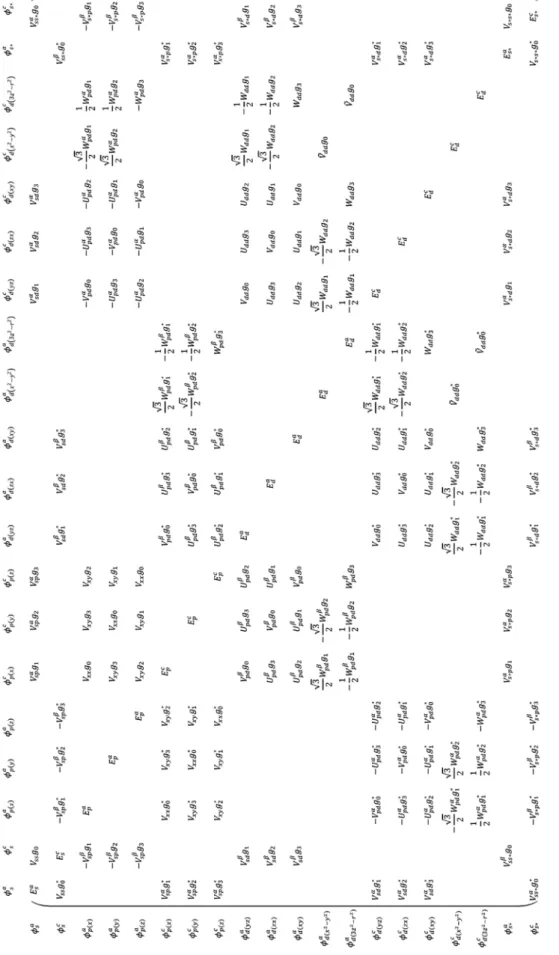
zinc-blende crystal structure. Figure 1 shows the resulting 20 × 20 Hamiltonian matrix. Matrix entries are calculated as follows:
Vss= Vss𝜎 Vsp= −√1 3 Vsp𝜎 Vxx= 1 3Vpp𝜎+ 2 3Vpp𝜋 Vxy= 1 3Vpp𝜎− 1 3Vpp𝜋 Vsd= √1 3 Vsd𝜎 Vpd= 1 3 � Vpd𝜎−√2 3 Vpd𝜋 � Upd= 1 3 � Vpd𝜎+ 1 √ 3 Vpd𝜋 � Wpd= 2 3Vpd𝜋 Vdd= 1 9 [ 3Vdd𝜎+ 2Vdd𝜋+ 4Vdd𝛿 ] ̃ Vdd= 1 3 [ 2Vdd𝜋+ Vdd𝛿 ] Udd= 1 9 [ 3Vdd𝜎 − Vdd𝜋− 2Vdd𝛿 ] Wdd= 2 3√3 � −Vdd𝜋+ Vdd𝛿�.
The α and β superscripts used in Fig. 1 define whether it refers to an anion-to-cation integral or a cation-to-anion one. Diagonal elements (Eii) denote the self-integrals of
the orbitals. The s* integrals use the same notation of the
s ones. The gi are the phase factors that take into account
the fact that we are evaluating integrals with respect to each nearest neighbor, which are defined as:
w h e r e R1= [ −a2,−a2, 0 ] , R2= [ 0,−a2,−a2 ] , R1=[−a 2, 0,− a 2 ]
, and a is the lattice constant.
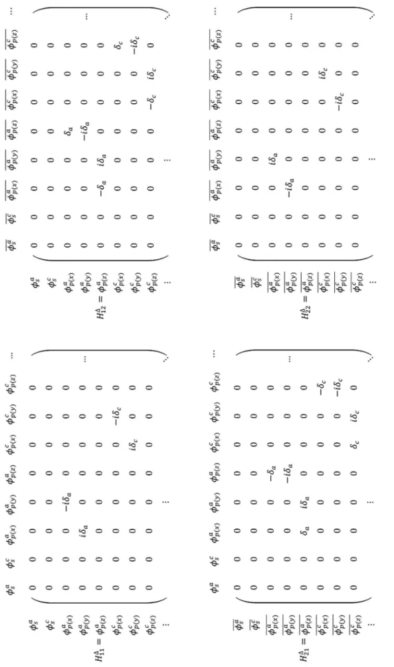
Spin–orbit coupling
In this model, we also take into account the spin–orbital coupling between p orbitals as explained by Datta [13]. Spin-orbit interaction is responsible for lifting the degen-eracy of the valence band and plays a role in defining the optical properties of the material [6]. In this work, we considered only the contribution of p valence states since that of the excited d states is much smaller [12].
The introduction of spin–orbit interaction in the model is implemented distinguishing between ↑ and ↓ electrons and creating a matrix twice the rank with the introduc-tion of two coupling parameters δa and δc (where 𝛿a,c =
Δa,c∕3 ). Such a 40 × 40 Hamiltonian matrix, H, can be defined starting from a matrix having two of the 20 × 20
Hsp3d5s∗ matrices portrayed in Fig. 1 as diagonal elements and adding it to a coupling matrix HΔ:
where HΔ
ij are defined in Fig. 2.
Verification of the model
The model involving sp3d5s∗+ Δ parameters has
previ-ously been applied to a set of semiconductors in Ref. [12]. As a verification of the model construction and optimiza-tion procedure of the coupling parameters, here we dem-onstrate the results obtained for GaAs. Table 1 shows that the coupling parameters and the accuracy of our model are comparable to those reported in Ref. [12].
g0= 1 + e−ikR1+ e−ikR2+ e−ikR3
g1= 1 + e−ikR1− e−ikR2− e−ikR3
g2= 1 − e−ikR1+ e−ikR2− e−ikR3
g3= 1 − e−ikR1− e−ikR2+ e−ikR3
H= [ Hsp3d5s∗ 0 0 Hsp3d5s∗ ] + [ HΔ 11 H Δ 12 HΔ21 HΔ22 ]
Fig . 1 20 × 20 Hsp 3d 5s ∗ matr ix
Journal of Theoretical and Applied Physics
1 3
Fig . 2 Spin–orbit matr ixOptimization for SiC
Following the construction of the matrix, an optimization proce-dure is necessary to find the SETBM parameters for any given material. Here we provide a method that can be generalized to other materials as well. The optimization requires experimental data on energy levels at high symmetry points and effective masses in certain directions, a well-designed cost function, and finally a physically meaningful initial point. As described in Ref. [12], a good candidate for the initial point is the free elec-tron model-generated parameters for the coupling energies. We have also observed that using other zincblende structures’ cou-pling parameters as initial points produced good results.
We have built our cost function to take into account both energy levels and effective masses at the same time. Since the cost comprises of points and curvatures to fit, this ensures a physically meaningful band diagram when initiated from the points described above. Following the definition of this cost function, we perform constrained nonlinear optimization using the Nelder–Mead simplex algorithm [14]. Other optimization methods such as genetic algorithms are found to be inefficient for this approach since the problem structure is sufficiently bounded and thus does not need a high level of exploration.
Results
Using the model described above, here we present the electronic band structure and the corresponding density of states calculated for 3C-SiC. Table 2 shows a comparison between the experimental values of high symmetry points Table 1 Comparison between experimental values of the GaAs high symmetry points and effective masses, the corresponding values eval-uated by Jancu et al. in Ref. [12] using SETBM and the same value evaluated using our model
Parameter Previous work [12] This work Experimental [6] Γ6v −12.910 eV −13.070 eV −13.1 eV
− Δ0 −0.340 eV −0.339 −0.341 eV
Γ6c 1.519 eV 1.519 eV 1.519 eV
Γ7c 4.500 eV 4.497 eV 4.53 eV
Γ8c 4.716 eV 4.764 eV 4.716 eV
X6v −3.109 eV −2.904 eV −2.88 eV X7c −2.929 eV −2.790 eV −2.80 eV
X6c 1.989 eV 2.009 eV 1.98 eV
X7c 2.328 eV 2.385 eV 2.35 eV
L6v −1.330 eV −1.427 eV −1.42 eV L4,5v −1.084 eV −1.180 eV −1.20 eV
L6c 1.837 eV 1.829 eV 1.85 eV
L7c 5.047 eV 5.303 eV 5.47 eV
m(𝛤
6c
) 0.067 m
0 0.067 m0 0.067 m0
Avg. accuracy 97.11% 99.45% 100%
Table 2 Comparison between experimental values of the SiC high symmetry points and effective masses, the corresponding values eval-uated by Theodorou et al. in Ref. 6 using SETBM and the same value evaluated using our model
Parameter Previous work
[6] This work Experimental [6]
∆0 – − 10.3600 meV − 10.36 meV
Γ1c 7.07 eV 7.4000 eV 7.40 eV
Γ15c 8.98 eV 7.7253 eV 7.75 eV
X5v − 3.2 eV − 3.5977 eV − 3.60 eV
X1c 2.47 eV 2.3900 eV 2.39 eV
X3c 5.64 eV 5.5000 eV 5.50 eV
L3v − 1.18 eV − 1.1522 eV − 1.16 eV
L1c 6.22 eV 5.9400 eV 5.94 eV
L3c 9.11 eV 8.5004 eV 8.50 eV
m∥ – 0.6700m0 0.67m0
m⊥ – 0.2500m0 0.25m0
Avg. Accuracy 93.6% 99.91% 100%
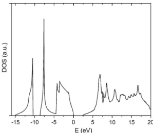
Fig. 3 Electronic band structure for SiC calculated with the sp3d5s* + Δ model. Experimental values reported in Ref. [6] are noted
with red dots
Fig. 4 Density of states of SiC calculated with the sp3d5s* + Δ model
Journal of Theoretical and Applied Physics
1 3
and effective masses and the same values calculated using our model and a previous SETBM implementation from Theodorou et al. [6]. Figure 3 shows that the conduction band minimum is at X point giving an indirect band structure with a bandgap of 2.39 eV. The optimized model predicts the experimental results with a reasonably high average accu-racy of 99.91%. Other than the high symmetry points, it can also be noticed that the band diagram shows a constant gap in the Λ direction between valence and conduction bands as expected from reflectivity measurements [15]. Coupling parameters optimized for 3C-SiC are listed in Table 2, while the density of states diagram is shown in Fig. 4.
Specifically, for the band diagram of 3C-SiC, the spin–orbit coupling does not play a major role as the splitting of the valence bands is 10.3 meV. The effect becomes more important when other physical parameters, such as dielectric function [6], are of interest. Mainly, not to lose the generality of the model,
this effect is included in all of the calculations, obtaining small spin–orbit coupling parameters ( 𝛿a, 𝛿c ) as expected (Table 3).
Conclusion
We have reported the full implementation of a semiempiri-cal tight-binding model for zincblende 3C-SiC with sp3d5s*
orbitals and spin–orbit coupling (∆). Model parameters ini-tialized using free electron model parameters and optimized using experimental energy values and effective masses have shown 99.91% average accuracy. Construction of the matrix and the optimization procedure can be further applied to other materials, in describing their electronic properties. Acknowledgements The authors would like to acknowledge Prof. Qing Hu from Massachusetts Institute of Technology for the helpful discus-sions and guidance.
Open Access This article is distributed under the terms of the Crea-tive Commons Attribution 4.0 International License (http://creat iveco
mmons .org/licen ses/by/4.0/), which permits unrestricted use,
distribu-tion, and reproduction in any medium, provided you give appropriate credit to the original author(s) and the source, provide a link to the Creative Commons license, and indicate if changes were made.
References
1. Harris, G.L.: Properties of Silicon Carbide. INSPEC, London (1995) 2. Shur, M., Rumyantsev, S., Levinshtein, M.: SiC Material and
Devices. World Scientific, Singapore (2006)
3. Fan, J., Chu, P.K.-H.: Silicon Carbide Nanostructures. Springer, Berlin (2014)
4. Saddow, S.E., Agarwal, A.: Advances in Silicon Carbide Processes and Applications. Artech House, Norwood (2004)
5. Kackell, P., Wenzien, B., Bechstedt, F.: Phys. Rev. B 50, 10761 (1994)
6. Theodorou, G., Tsegas, G., Kaxiras, E.: J. Appl. Phys. 85, 2179 (1999)
7. Lubinsky, A.R., Ellis, D.E., Painter, G.S.: Phys. Rev. B 11, 1534 (1974)
8. Junginger, H.-G., van Haeringen, G.: Physica Status Solidi 37, 709 (1970)
9. Hemstreet, L.A., Fong, C.Y.: Phys. Rev. B 6, 1464 (1972) 10. Vogl, P., Halmarson, H.P., Dow, J.D.: J. Phys. Chem. Solids 44, 365
(1981)
11. Slater, J.C., Koster, G.F.: Phys. Rev. 94, 1498 (1954)
12. Jancu, J.M., Sholz, R., Beltram, F., Bassani, F.: Phys. Rev. B 57, 6493 (1998)
13. Datta, S.: Quantum Transport: Atom to Transistor. Cambridge Uni-versity Press, Cambridge (2005)
14. Lagarias, J.C., Reeds, J.A., Wright, M., Wright, P.E.: Soc. Ind. Appl. Math. J. Optim, 9, 112 (1998)
15. Madelung, O., von der Osten, W., Rossler, U.: Intrinsic Properties of Group IV Elements and III-V, II-VI and I-VII Compounds. Springer, Berlin (1987)
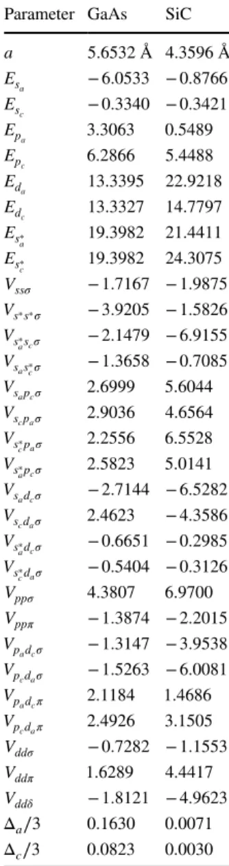
Publisher’s Note Springer Nature remains neutral with regard to jurisdictional claims in published maps and institutional affiliations. Table 3 Fitting parameters
optimized for GaAs and SiC Parameter GaAs SiC a 5.6532 Å 4.3596 Å Es a − 6.0533 − 0.8766 Es c − 0.3340 − 0.3421 Epa 3.3063 0.5489 Ep c 6.2866 5.4488 Ed a 13.3395 22.9218 Edc 13.3327 14.7797 Es∗ a 19.3982 21.4411 Es∗ c 19.3982 24.3075 Vssσ − 1.7167 − 1.9875 Vs∗s∗𝜎 − 3.9205 − 1.5826 Vs∗ asc𝜎 − 2.1479 − 6.9155 Vs as∗c𝜎 − 1.3658 − 0.7085 Vsapc𝜎 2.6999 5.6044 Vs cpa𝜎 2.9036 4.6564 Vs∗ cpa𝜎 2.2556 6.5528 Vs∗ apc𝜎 2.5823 5.0141 Vsadc𝜎 − 2.7144 − 6.5282 Vs cda𝜎 2.4623 − 4.3586 Vs∗ adc𝜎 − 0.6651 − 0.2985 Vs∗ cda𝜎 − 0.5404 − 0.3126 Vppσ 4.3807 6.9700 Vppπ − 1.3874 − 2.2015 Vp adc𝜎 − 1.3147 − 3.9538 Vpcda𝜎 − 1.5263 − 6.0081 Vp adc𝜋 2.1184 1.4686 Vp cda𝜋 2.4926 3.1505 Vddσ − 0.7282 − 1.1553 Vddπ 1.6289 4.4417 Vddδ − 1.8121 − 4.9623 Δa∕3 0.1630 0.0071 Δc∕3 0.0823 0.0030