Charge and Energy Transport in OD/2D Systems
Probed Using Linear and Nonlinear Spectroscopy
by
Aaron J. Goodman
Submitted to the Department of Chemistry
in partial fulfillment of the requirements for the degree of
Doctor of Philosophy
in Physical Chemistry
at the
MASSACHUSETTS INSTITUTE OF TECHNOLOGY
June 2018
@
Massachusetts Institute of Technology 2018. All rights reserved.
Author ...
Signature redacted
Department of Chemistry
May 17, 2018
Signature redacted
C ertified by ...
William A. Tisale
Associate Professor without Tenure
Thesis Supervisor
Signature redacted
A ccepted by ...
Robert W. Field
Chairman, Department Committee on Graduate Theses
MASSACHUSETTS INSTITUTE OF TECHNOLOGY
JUN
2 02018
Charge and Energy Transport in OD/2D Systems Probed
Using Linear and Nonlinear Spectroscopy
by
Aaron J. Goodman
Submitted to the Department of Chemistry on May 17, 2018, in partial fulfillment of the
requirements for the degree of Doctor of Philosophy
Abstract
Low-dimensional nanostructured semiconductors are promising technologies for next generation optoelectronics. Colloidal quantum dots (QDs) have been applied in many light emitting applications such as ambient lighting downconverters, LEDs, and displays. Proof-of-concept transistors, phototransistors and LEDs have been demonstrated using two dimensional atomically thin transition metal dichalcogenides (TMDs). To realize efficient next generation optoelectronics using these materials it is crucial to understand the dynamics and transport of energy and charge in these ma-terials and hybrid structures built from them. The first Chapter of this thesis briefly motivates the technological importance of QDs and TMDs. The remainder explores exciton dynamics and transport in these low-dimensional semiconductor systems.
In Chapter 2, low temperature spectroscopy and time-resolved photoluminescence spectroscopy are used to probe the complex energy landscape seen by excitons in acid-treated MoS2. We show that deeply trapped "dark" exciton states are
responsi-ble for the surprisingly long lifetime of band-edge photoluminescence in acid-treated
single-layer MoS2. Temperature-dependent transient photoluminescence spectroscopy
reveals an exponential tail of long-lived states extending hundreds of meV into the band gap. These subband states, which are characterized by a 4 pus radiative lifetime, quickly capture and store photogenerated excitons before subsequent thermalization up to the band edge where fast radiative recombination occurs. By intentionally satu-rating these trap states, we are able to measure the "true" 150 ps radiative lifetime of the band-edge exciton at 77 K, which extrapolates to -600 ps at room temperature. These experiments reveal the dominant role of dark exciton states in acid-treated
MoS2, and suggest that excitons spend > 95% of their lifetime at room temperature in trap states below the band edge. We hypothesize that these states are associ-ated with native structural defects, which are not introduced by the superacid treat-ment; rather, the superacid treatment dramatically reduces nonradiative recombina-tion through these states, extending the exciton lifetime and increasing the likelihood of eventual radiative recombination.
using time-resolved diffusion imaging. We also probe exciton-exciton dynamics and elucidate the role that exciton traps play in both exciton transport and dynam-ics. Atomically thin semiconductors such as monolayer MoS2 and WS2 exhibit
non-linear exciton-exciton annihilation at notably low excitation densities (below ~10 excitons/pm2 in MoS2). We show that the density threshold at which annihilation
occurs can be tuned by two orders of magnitude by varying the refractive index of the underlying supporting substrate. Using spatially-resolved transient photolumi-nescence spectroscopy in conjunction with numerical simulations, we find that this behavior arises from screening interactions between trapped and mobile exciton pairs. We measure the effective exciton diffusion coefficient in superacid-treated MoS2 to be
D = 0.06 0.01 cm2
/s, corresponding to a diffusion length of LD = 350 nm for an
exciton lifetime of T = 20 ns. Exciton-exciton annihilation limits the overall efficiency
of 2D semiconductor devices operating at high exciton densities. The ability to tune these interactions via the dielectric environment is an important step toward more efficient optoelectronic technologies featuring atomically thin materials.
In Chapter 3 we investigate coupled QD/TMD hybrid structures. In the first half of Chapter 3, we investigate dipole-dipole coupling in the regime that the QD and TMD exhibit weak electronic coupling by engineering the interface to be insulating. We report highly efficient F6rster resonant energy transfer from cadmium selenide (CdSe) quantum dots to monolayer and few-layer molybdenum disulfide (MoS2). The
quenching of the donor quantum dot photoluminescence increases as the MoS2 flake
thickness decreases with the highest efficiency (> 95%) observed for monolayer MoS2.
This counterintuitive result (that deviates from the predictions of F6rster theory) arises from reduced dielectric screening in thin layer semiconductors having unusually large permittivity and a strong in-plane transition dipole moment, as found in MoS2.
In the second half of Chapter 3, we investigate QD/TMD hybrid structures in the strongly coupled regime. We demonstrate tunable electronic coupling between CdSe QDs and monolayer WS2 using variable length alkanethiol ligands on the QD surface.
Using femtosecond time-resolved second harmonic generation (SHG) microscopy, we show that electron transfer from photoexcited CdSe QDs to single-layer WS2 occurs on
ultrafast (10 fs - 1 ps) timescales. Moreover, charge transfer excites coherent acoustic phonons in the donor QDs, which modulate the SHG response of the underlying WS2
layer on picosecond timescales. These results reveal surprisingly strong electronic coupling at the QD/TMD interface and demonstrate the usefulness of time-resolved
SHG for exploring ultrafast electronic-vibrational dynamics in TMD heterostructures.
In Chapter 4, we improve the sensitivity of traditional SHG spectroscopy by adding an additional field. We demonstrate the dramatic enhancement of weak second-order nonlinear optical signals via stimulated sum and difference frequency generation. We present a conceptual framework to quantitatively describe the interaction and show that the process is highly sensitive to the relative optical phase of the stimulating field. To emphasize the utility of the technique, we demonstrate stimulated enhance-ment of second harmonic generation (SHG) from bovine collagen-I fibrils. Using a stimulating pulse fluence of only 3 nJ=cm2, we obtain an SHG enhancement > 104
relative to the spontaneous signal. We discuss the conceptual differences between optical heterodyning of SHG signals and our presented "stimulation" framework. In
the second half of Chapter 4, we use the additional field to resolve the SHG signal phase revealing the sign and magnitude of the sample nonlinear susceptibility. We perform phase-resolved SHG imaging of polycrystalline MoS2 flakes and determine
the absolute grain orientations using the phase information. Thesis Supervisor: William A. Tisale
Acknowledgments
I would like to thank sources of financial funding that made my Ph.D. possible.
Thanks to the National Science Foundation for paying my stipend through the Grad-uate Research Fellowship Program, to the Department of Energy for funding much of my research through Will's Early Career Award and through the Center for Exciton-ics, an Energy Frontier Research Center at MIT and Harvard. Thanks to the Samsung Global Research Opportunities program for funding work investigating charge trans-fer at QD/TMD interfaces.
Countless thanks to Will for being an outstanding advisor. In a very practical sense, Will always enables his students to do good science: he provides funds, creativ-ity, and rigorous scientific thinking all of which are important in creating a successful research environment. I know that I pursued a few hare-brained ideas; Will enabled that exploration even when it didn't directly address an existing research goal. I es-pecially enjoyed and valued the scientific conversations in which we solved problems collaboratively. Perhaps most importantly, Will always puts the needs and goals of his students first valuing their success rather than treating them as a means to an end (this is surprisingly uncommon at MIT). He does this conscientiously and with great kindness. I also thank him for actively creating an inclusive work environment where all group members feel welcome. I couldn't have asked for a better group of coworkers and that starts at the top.
My thesis committee has helped me immensely. Professor Nelson has provided
valuable insight. I always enjoyed our annual meeting; his passion for science is unmatched and his deep understanding of ultrafast optics made our research discus-sions a true pleasure. Professor Bawendi contributed considerable expertise in the physics of nanostructured materials. Talking with him and his group members really strengthened my knowledge of exciton transport and dynamics empowering me to complete this work.
Special thanks to Ferry Prins for being a mentor and friend in the Tisdale group. Ferry brought two dimensional TMDs into the group and spearheaded the QD/TMD
energy transfer story. Additionally, Ferry was an enthusiastic, capable mentor and force for positive culture in the group during the formative early years. Though there is stiff competition, Ferry may have been the most capable drinking partner to grace the Muddy Charles with me.
In a tie for close second are Dr. Mark Weidman and Leo Spiegel. Mark is a phenomenal scientist whose productivity is a thing of Tisdale Lab legend. Mark helped train me on the diffusion imaging apparatus that he and Matt built together and was a valuable collaborator and friend.
Yunan Gao (Steve, the first of his name) was another outstanding postdoctoral re-searcher who developed the phase-resolved degenerate parametric amplification tech-nology to completion and made important contributions to my pump-probe SHG optical setup. Yunan thought about science in a creative and simultaneously pre-cise way and we shared many stimulating discussions. I appreciate his kindness and friendship.
Dr. Jolene Mork was a fantastic mentor who was always willing to help me. I appreciate her willingness to not take things too seriously and her companionship that one time we were stranded in Texas. With her considerable wet lab expertise she set many good precedents that made the lab more safe and productive, and was a willing aid when I had to do things with chemicals.
Thanks to Dr. Rachel Gilmore for teaching me ultrafast optics and for building the ultrafast bay from scratch. I appreciate her willingness to take things just seriously enough. The depth and completeness with which she answered her scientific questions always impressed me. I am glad to have her as a friend.
Thanks Matt Ashner for introducing me to climbing. He probably increased my life expectancy by showing me a physical activity that captures my imagination and reduces my stress. He is an ambassador to the sport.
Thank you to all of the other Tisdale Lab members for being talented, wonderful coworkers and collaborators. Nabeel thank you for tirelessly taking point making sure the lab continued to function. Sam, thank you for being an even better social chair than I could ever hope to be. Liza, thank you for your piercing insight and for your
friendship. Thank you for members of the Gossip Club for gossiping with me. For the last two years, Michelle and I have lived in East Campus on 41W. Thank you to Rob Miller, Sandy Alexandre, and Carrie Wicks for being a supportive house team. Each cares deeply about the students in East Campus and provided bottomless support for the Graduate Resident Tutors (GRTs) there. Likewise, the other GRTs are beautiful people whom I'm glad to know. Living on 41W has taught me to practice my empathy and also made me question some of my assumptions. It is special to live in a community where everyone is accepted as their authentic self.
I was lucky to work in Professor Bart Bartlett's lab at the University of Michigan. My experience there drove me to start my graduate studies by showing me how fun
basic research could be. Bart was a formative undergraduate advisor who never compromised and produced good science as a result. I appreciate the opportunity to work in his lab.
Thank you to my dear friends Adam, David, Max, Russ, Sean, and Ted. You offer consistent support when things are difficult. Thanks for being there.
While at MIT, I met and married my best friend Michelle. Thank you Michelle for always supporting me, convincing me of my worth, and loving me unconditionally. We make a good team, and I look forward to what comes next.
My family has always supported me in my endeavors. Thanks to my parents for
providing me with a safe home and a college education. I broke a lot of things in our house when I did "science" "experiments", and my parents were generally supportive of that creativity. Thank you to Sarah and David for being wonderful siblings who always want the best for me. I love you guys.
Buddy
tail wagging at work
he is happy that you're here he will steal your food.
This doctoral thesis has been examined by a Committee of the
Department of Chemistry as follows:
Professor Keith A. Nelson...Signature
redacted
Chairman, Thesis Committee
Haslam and Dewey Professor of Chemistry
Signature
redacted-Professor William A. Tisdale.
...
Thesis Supervisor
ARCO Career Development Associate Professor of Chemical
Engineering
Signature redacted
Professor Moungi G. Bawendi...
...
Member, Thesis Committee
Lester Wolfe Professor of Chemistry
Contents
1 Motivation for Low Dimensional Materials 35
1.1 2D TMDs for Lighting and Computing ... 35
1.2 Quantum Dots for Displays and Lighting ... ... 38
2 Exciton Transport and Dynamics in Transition Metal Dichalcogenide Monolayers 41 2.1 Excitons in Transition Metal Dichalcogenides . . . . 41
2.1.1 Exciton Background Information . . . . 41
2.1.2 Transition Metal Dichalcogenides Background . . . . 43
2.2 Exciton Trapping Is Responsible for the Long Apparent Lifetime in Acid-Treated M oS2 . . . . 45
2.2.1 Background for Chemical Treatment of MoS2 Samples . . . . 45
2.2.2 Background for Radiative Rates and Apparent Decay Rates in TMDs... ... 47
2.2.3 Trapped Exciton States in MoS2 . . . . . . . . 49
2.2.4 Equilibration between Band-Edge and Trapped Exciton States 51 2.2.5 Observing the True Radiative Rate . . . . 53
2.2.6 Numerical Modelling Details and Results . . . . 56
2.2.7 Trap States in CVD-Grown MoS2 . . . . 58
2.2.8 Conclusions . . . . 59
2.2.9 Experimental Methods . . . . 61
2.3 Suppressing Diffusion-Mediated Exciton-Exciton Annihilation in 2D Semiconductors Using the Dielectric Environment . . . . 62
2.3.1 Exciton Exciton Annihilation . . . . 62
2.3.2 Exciton Diffusion . . . . 64
2.3.3 Supressing Exciton-Exciton Annihilation . . . . 66
2.3.4 Measuring Exciton Diffusion in TMDs . . . . 69
2.3.5 Exciton Trapping Influences Exciton Transport and Annihilation . . . . 73
2.3.6 Results and Conclusions . . . . 77
2.3.7 Exciton Diffusivity Measurements: MoS2 on Sapphire and STO 81 2.3.8 Generation Rate Dependent Quantum Yield in WS2 . . . . . . 81
2.3.9 Optical System Characterization . . . . 82
2.3.10 PL Spectra Under Extended Vacuum and Cooling . . . . 83
2.3.11 Fitting Low Temperature PL Spectra . . . . 85
2.3.12 Experimental Methods . . . . 86
3 2D/OD Hybrid Structures: CdSe Quantum Dots on Transition Metal Dichalcogenides 89 3.1 Hybrid Quantum Dot / 2D Devices . . . . 89
3.2 Exciton States in Transition Metal Dichalcogenides and Quantum Dots 91 3.2.1 Transition Metal Dichalcogenide Electronic Structure . . . . . 91
3.2.2 CdSe Quantum Dot Electronic Structure . . . . 95
3.3 Reduced Dielectric Screening and Enhanced Energy Transfer in Single-and Few-Layer MoS2 . .. . . . . . . 97
3.3.1 Fdrster Resonance Energy Transfer . . . . 97
3.3.2 Measuring the Rate of Energy Transfer Using Time-Correlated Single Photon Counting . . . . 99
3.3.3 Energy Transfer in CdSe/CdZnS Quantum Dot/MoS2 Hybrid Structures . ... ... ... . . . 101
3.3.4 Conclusions . . . . 108
3.3.5 Energy Transfer from to MoS2 from QDs with Thin Shells and Short Ligands . . . . 110
3.4 Theory of Charge Transfer in OD/2D Donor/Acceptor Systems . . . . 111
3.5 Charge Transfer in CdSe Quantum Dot/WS2 Monolayer Heterostructures 113 4 Stimulated Second Harmonic Generation 123 4.1 Second Harmonic Generation . . . . 123
4.2 Optical Stimulation Background . . . . 126
4.3 Enhancement of Second-Order Nonlinear-Optical Signals by Optical Stim ulation . . . . 128
4.3.1 Second Order Nonlinear Optical Spectroscopies: Successes and O pportunities . . . . 128
4.3.2 Amplifying the Second Harmonic Generation Signal: Results . 130 4.4 Philosophical and Practical Differences between Optical Stimulation and Heterodyne Detection . . . . 137
4.4.1 Comparing Optical Stimulation to Heterodyne Detection . . . 137
4.4.2 Contrasting Optical Stimulation to Heterodyne Detection . . . 139
4.5 Phase-Sensitive Nonlinear Optical Imaging of Two-Dimensional Materials 141 4.5.1 Phase-Sensitive Imaging of 2D Materials . . . . 143
4.5.2 Spatial Resolution of DPA . . . . 146
4.5.3 Conclusion . . . . 147
List of Figures
1-1 Members of the layered TMD family typically possess one of three crystallographic symmetries (2H, IT, or iT'). The thermodynamically favored structural phase depends on material composition with some compositions possessing metastable phases. . . . . 36
1-2 (a) CIE chromaticity digram. QDs exhibit narrow emission line widths and can be tuned to emit across the visible spectrum. Their color pu-rity allows mixtures of dots to accurately reproduce a large fraction of the humany perceivable color space. (b) Plot showing luminous efficacy (lm W-1) and color rendering index (CRI, a metric indicating a light source's ability to accurately render colors). Due to their color pu-rity and spectral tunability QD-based ambient lighting devices can be engineered with good luminous efficiency and CRI. Figure reproduced from ref. [1], Nature Publishing Group . . . . 39
2-1 Exciton varieties. (a) Bulk Wannier-Mott exciton (b) Bulk Frenkel
ex-citon (c) An exex-citon confined in one dimension (d) An exex-citon confined in three dim ensions . . . . 42 2-2 Acid-treated MoS2 optical properties at room temperature. (a) The
ab-sorbance spectrum (blue) shows two sharp, excitonic resonances arising from the A and B excitons that originate from the K point in the Bril-luoin zone. (b) Time-correlated single photon counting histogram of the A exciton photoluminescence at room temperature exhibits single-exponential decay dynamics with a time constant, Tobs = 20 ns. . . . . 47
2-3 Temperature-dependent photoluminescence spectra (a) Photolumines-cence spectra (thin lines) at low temperature exhibit emission at en-ergies below the band-edge exciton. The lineshape is fit well by an exponential density of states occupied by a Fermi-Dirac Distribution (thick lines). (b) At low temperature, trapped exciton emission domi-nates the photoluminescence spectra, while at high temperatures most luminescence comes from the band-edge exciton. (c) Power-dependent photoluminescence spectra at 77 K reveal that the band-edge exciton emission becomes more prominent relative to the trapped exciton emis-sion at higher laser powers. This observation indicates that a significant portion of the traps are filled at moderate excitation intensities. . . . 50
2-4 A three-state model explains the observed photoluminescence decay
time and the absence of trap state emission at room temperature. (a) Apart from the ground state and the band-edge exciton, there are also trapped exciton states that have -1000x slower recombination rate than the band-edge exciton. At room temperature, thermalization up to the band edge and subsequent radiative recombination is most probable, whereas at 77 K direct recombination from trap to ground state is observed. (b) Time-resolved trapped exciton emission reveals these two pathways. At 77 K, trapped excitons decay with their slow radiative rate (- 4 ps). At higher temperatures, some thermalize up to the band-edge leaving behind only deeply trapped excitons, which decay slowly. The shaded region of the inset indicates the portion of the spectrum that is collected by the time-resolved detector. . . . . . 52
2-5 Spectrally-resolved transient photoluminescence spectroscopy reveals the true radiative rate. (a) At room temperature, nearly all of the emission comes from the band-edge exciton, with a noticeable con-tribution from the B exciton. The exciton emission has long-lived components mediated by the long-lived, dark trapped exciton states.
(b, c) At 77 K, the majority of emission comes from trapped excitons (~ 1.65- 1.85 eV). The pulsed laser operates at 76 MHz (13 ns between
pulses), so the long-lived trapped exciton sites are always nearly com-pletely occupied in this experiment. When a new pulse arrives, band edge excitons cannot trap and instead decay radiatively with a rate reflecting the true band-edge radiative rate, which is 150 ps at 77 K. . 55
2-6 Power-dependent PL at 77 K. Power-dependent PL spectra (light gray) were fitted to band edge and trapped exciton contributions (colored lines) to extract density-dependent steady state populations. . . . . . 56
2-7 Transient photoluminescence modelling. (a) The trap state energy spectrum used in the numerical model is illustrated here. The PL spectrum is plotted in red with the x-axis energy centered about the band edge exciton energy, Ex. The density of trap states is exponen-tially decaying from the band edge with a slope a = 5 eV-1
found from fitting the PL spectra. This exponential decay is plotted in blue. The transient ODE model was solved five times at each temperature with trap state energies represented by the blue rectangles. The weight of each solution parameterized by a specific trap state energy was deter-mined by the density of states. The five solutions for each temperature were added together to generate the model's output. (b) The exper-imental trapped exciton emission at multiple temperatures is plotted along with the model output, which was generated with no free param-eters. . . . . 58
2-8 Temperature dependent PL spectra from acid-treated CVD-grown MoS2.
The CVD-grown sample also exhibits trapped exciton emission at low temperature. The trapped exciton emission line shape differs reflecting a different energetic distribution of trap states. . . . . 58 2-9 Proposed superacid treatment mechanism. The TFSI acid chemically
oxidizes the MoS2, removing dopant electrons. The conjugate base
anion then passivates the structural defect. . . . . 59
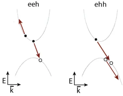
2-10 Three carrier Auger processes (left) A relaxing electron scatters off another electron promoting increasing its energy (right) A relaxing electron scatters off of a hole, pushing it deeper into the valence band. In each case, energy and momentum are conserved. . . . . 63
2-11 Effect of substrate on the optical properties of superacid-treated MoS2. (a) Transmission optical micrograph of exfoliated MoS2 with monolayer
region indicated. The inset depicts the chemical structure of the su-peracid used in the treatment. The dark thick line is the border of the polymer capping layer on top of the MoS2 flake. (b) Schematic
of the substrate/MoS2
/polymer
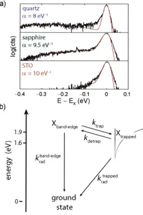
stack. (c) Photoluminescencespec-tra of treated MoS2 on quartz (blue), sapphire (green), and STO
(red). (d) Steady-state QY measured as a function of exciton
gen-eration rate. Data were recorded for MoS2 supported on quartz (blue
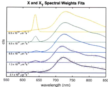
trace), sapphire (green trace), and strontium titanate (red trace). (e) Time-resolved photoluminescence traces. The traces were globally fit to extract kx and kxx as described in the text. (f) Exciton-exciton an-nihilation rate constants, kxx, inferred from steady-state QY ments (open circles) and time-resolved photoluminescence measure-ments (filled squares). kxx values for MoS2 on quartz (blue), sapphire
(green), and strontium titanate (red) are plotted against the supporting substrates' refractive indices (top). Analogous data for WS2 samples
2-12 Exciton diffusion imaging. (a) Schematic diagram of the optical ap-paratus used to resolve exciton diffusion in space and time. (b) top: simulation of the photoluminescence intensity along a line cut of the radially symmetric exciton population as a function time. With an incident fluence of 0.5 nJ/cm2
, almost all excitons decay radiatively and the spot broadens due to diffusion. bottom: same as top panel, but with an incident fluence of 50 nJ/cm2
, many excitons decay due to annihilation. This results in artificial broadening of the density profile; excitons decay most rapidly in the center of the spot where exciton density is highest. (c) Experimentally observed broadening of the ex-citon population with time at 0.5 nJ/cm2, 5 nJ/cm2, and 50 nJ/cm2 incident fluences in the top, middle, and bottom panels, respectively. White lines indicate the evolution of the standard deviation with time.
(d) Steady-state measurement of exciton diffusion. The intensity
pro-file of luminescence coming from a film of quantum dots is indicated in green. Excitons do not diffuse in this sample, so the intensity profile indicates the performance of our optical system. The photolumines-cence intensity profile collected from MoS2 with a generation rate of
4.8 x 1015 cm-2s-1 is broadened due to diffusion. The diffusive contri-bution to the width of the intensity districontri-bution is indicated in red in the inset. (e) This cartoon illustrates the role that trapped excitons play in influencing the measured diffusivity. Though excitons diffuse quickly at the band edge with the band edge diffusivity, they fall into immobile traps. Consequently the measured diffusivity (Dmeasured) is
2-13 Trapped exciton states and their equilibration with the band edge. (a) 77 K photoluminescence spectra of MoS2 supported on quartz (top),
sapphire (middle), and strontium titanate (bottom). At low temper-ature, trapped excitons emit at energies below the free exciton. The photoluminescence spectra (solid black lines) are modelled as a Fermi-Dirac distribution over an exponential density of states. (b) State diagram for trapped and band-edge (free) excitons. . . . . 75
2-14 Monte Carlo simulation of trapped excitons contributing to annihi-lation. (a) Diffusing excitons meet long-lived trapped excitons and annihilate. The equilibrium between trapped and free excitons is re-sponsible for the large annihilation rate constants. (b) A Monte Carlo model invoking trapped and diffusing band edge excitons quantita-tively reproduces steady-state QY data. The model output is plot-ted here (thick transparent lines) against the experimental data (open circles) for MoS2 on quartz (blue), sapphire (green), and strontium
titanate (red). (c) The annihilation rate constant inferred from the model (crossed diamonds) is plotted along with the experimentally derived values (open circles, QY; filled squares, time-resolved photolu-minescence). The annihilation rate is plotted against the supporting substrates' refractive indices. . . . . 77
2-15 Screened Coulomb interactions in TMDs. The analytical form is
in-cluded as an inset. HO and Y are Struve and Bessel functions, re-spectively, Esub and epmma are the permittivity of the substrate and PMMA respectively, and ro is a characteristic screening length scale proportional to the TMD polarizability. . . . . 80
2-16 Diffusion imaging experiments performed on MoS2 supported on sap-phire (a), and STO (b). Top panels show the spatially-integrated PL decay. Middle panels show exciton diffusion imaging as discussed in 2.3.4. Bottom panels show the PL spatial distribution variance extracted from the middle panels evolving in time showing diffusive broadening. . . . . 81
2-17 Absolute quantum yield values for WS2 supported on quartz (green
circles), sapphire (yellow triangles), and STO (red squares) extracted from calibrated PL spectra as a function of carrier generation rate. The data are consistent with and qualitatively similar to the data for
MoS2 on the three substrates. At low generation rates, the samples emit with near unity quantum yield. As the generation rate increases, the exciton-exciton annihilation interaction lowers the quantum yield dram atically. . . . . 82
2-18 Optical imaging apparatus characterization. Left: PL image collected
from a thin film of well insulated CdSe quantum dots in which exciton diffusion does not occur. The dots were excited with a focused laser
(A = 520 nm, NA = 1.4). Middle: PL image collected from MoS2
with the same imaging system using a sufficiently low fluence to avoid exciton-exciton annihilation. Right: Radial intensity profiles of the images in the left and center panels showing that the MoS2 PL intensity profile is broadened due to exciton diffusion. . . . . 83 2-19 Photoluminescence spectra collected upon cooling (left) to and heating
(right) from liquid nitrogen temperature. The color gradation indicates temperature (room temperature is red, 77 K is blue). The cooling and heating cycle took approximately one hour. . . . . 84 2-20 Integrated photoluminescence intensity upon cooling (blue) to and
heating (red) from liquid nitrogen temperature. The cooling and heat-ing cycle took approximately one hour. . . . . 85
2-21 Schematic illustration of the two sub populations that contribute to low-temperature PL spectra. . . . . 86
3-1 QD/TMD hybrid devices (a) A proposed hybrid LED device in which
electrodes inject charges into the TMD. The charges meet and form excitons. Excitons transfer to the adjacent QD, which handles light emission. (b) A hybrid QD/TMD photodector takes advantage of the QDs tunable broadband absorption. The QD undergoes photoinduced charge transfer injecting free carriers into the TMD. The free carriers are swept out of the device by an applied field leading to photoinduced gain . . . . 9 1 3-2 (a) left: A molybdenum disulfide unit cell with lattice vectors a
1, a2. right: A 2D hexagonal lattice Brillouin zone with labelled critical
points as well as reciprocal lattice vectors b1, b2. (b) Band structure of monolayer MoS2 adapted from reference [2]. (c) Monolayer MoS2
differ-ential reflectance spectrum showing absorption features corresponding to the A and B excitons as well as interband transitions in the band nesting region, C . . . . 92 3-3 (a) Electric fields lines emanating from charges in atomically thin
TMDs can sample the surrounding dielectric environment, which is typically less polarizable than the TMD. (b) The Coulomb interaction between two point charges in a TMD is sensitive to the surrounding di-electric. Here the Coulomb potential energy due to two point charges separated by a distance ri is plotted. Bulk TMDs (such as MoS2)
are highly polarizable and the Coulomb potential is strongly screened (green). Quartz is much less polarizable and the Coulomb potential is less screened (blue). Charges in a MoS2 monolayer encased quartz
perience a Coulomb potential similar to charges separated in quartz ex-cept at very small distances, where the Coulomb potential approaches that of the bulk TMD (red). . . . . 94
3-4 (a) Colloidal quantum dots are nanometer-scale semiconductor crys-tallite cores covered with organic small molecule capping ligands that impart colloidal stability. (b) When the nanocrystal size is reduced below a critical size, the carriers begin to feel size-dependent quantum confinement effects. The continuous bands of states present in the bulk transition into atom-like discrete states near the band edge whose energies are sensitive to the quantum dot size. . . . . 96
3-5 Qualitative description of Fdrster resonant energy transfer (FRET) (a) FRET can be described as a donor dipole emitting a near field which is then received by a lossy acceptor dipole. The acceptor dipole must have some absorptive power by which to receive the radiated field. This interaction is screened by the intervening dielectric. (b) This analogy carries over to excitonic systems. Donor and acceptor dipoles corre-spond to the acceptor and donor transition dipole moments. Similarly to the macroscopic antenna picture, the dipoles are screened by a di-electric and must be aligned to facilitate energy transfer. . . . . 98
3-6 An excited quantum dot exhibits an effective decay rate, ktotai that is a sum of all the first order decay rates available to the exciton: the radiative rate krad, first order nonradiative rates kNR, and the energy transfer rate, kET. We can infer the energy transfer rate by measuring the total decay rate in the presence and absence of an energy acceptor. 99
3-7 Time-correlated single photon counting experimental apparatus. A
pulsed diode laser excites the sample. Emitted photons are directed to an avalanche photodiode (APD). Photon detection events at the APD result in a voltage pulse being sent to the counting board, which is synchronized to the laser excitation. Pulse arrival - photon emission delay times are recorded and histogrammed by the counting board. . 101
3-8 (a) Schematic of the hybrid QD/MoS 2 energy transfer system with indicated length scales. (b) Monolayer MoS2 absorption spectrum [3],
overlaid with the CdSe/CdZnS emission spectrum. Inset: transmission electron micrograph of a monolayer of the CdSe/CdZnS QDs used in this study. (c) Scanning electron micrograph showing the submono-layer of CdSe/CdZnS QDs on top of a MoS2 flake (dark section) and
the surrounding SiO2 substrate (lighter section). . . . . 102
3-9 (a) Optical micrograph of a mechanically exfoliated MoS2 flake with
indicated layer thicknesses of the different regions. (b) QD fluorescence lifetime map of the same flake with a saturated color scale to empha-size the lifetime variations within the flake area. (c) Energy transfer efficiency map of the same flake. . . . 103
3-10 (a) Fluorescence lifetime histograms of CdSe QDs on different
thick-nesses of MoS2. The black curve is obtained from
QDs
on top of SiO2.The dashed gray curve represents the instrument's response function. Inset: spectral overlap between CdSe QD emission and MoS2
absorp-tion spectra. (b) Same as (a) but for InAs quantum dots with an exciton resonance energy below the MoS2 exciton resonance. . . . . . 105
3-11 Energy transfer rate as a function of the number of MoS2 layers. The dashed line represents the energy transfer rate to thick, bulklike MoS2. Blue circles indicate experimental data with associated uncertainty that is smaller than the size of the symbols. The solid line is a fit to eqn. 3.10. Inset: schematic representation of the definition of the thickness (t) and distance (d) parameters. . . . 106
3-12 (a) Representative fluorescence lifetime histograms of the thin-shell
CdSe QDs on different thicknesses of MoS2. The black curve repre-sents the instrument's response function (IRF). Inset: spectral overlap between thin-shell CdSe QD emission and MoS2 absorption spectra.
(b) Enhancement factor as a function of t/d, where t is the underlying MoS2 thickness, and d is the distance from the quantum dot center to the MoS2 surface. Red circles represent the thin-shell quantum dot
data, which is in good agreement with the thick-shell quantum dot data presented in Fig. 3-11 in section 3.3.3 (blue circles) as well as with the fit of eqn. (3.10) (black line) to the thick-shell data. . . . .111
3-13 Characterization of the quantum dot (QD)/WS 2 heterostructure. (a)
Schematic of the QD/WS2 interface. QDs are coated with alkanethiol ligands of tunable length. (b) Estimated band alignment at the hybrid interface, based on published ionization potentials, exciton binding en-ergies, and measured optical gaps. (c) CdSe QD (dark, red) and WS2
(light, orange) absorption spectra. The pump pulse spectrum (black, dashed) selectively excites the quantum dots in the heterostructure. . 114
3-14 Time-resolved second harmonic generation (SHG). (a) Schematic of the time-resolved SHG microscopy instrument. (b) Transient SHG re-sponse of different samples. Data are shown for quantum dots capped with ethanethiol (blue, circles), butanethiol (green, squares), octanethiol (red, diamonds), and dodecanethiol (violet, triangles). Symbols repre-sent the experimental data, while transparent lines reprerepre-sent fits to a simple kinetic model. (c) Inverse electron transfer rate constants de-termined by fitting the data to our kinetic model. Values measured at different locations on the spatially heterogeneous sample are indicated
by open circles, while the average values are denoted by filled circles.
The gray line at the bottom of the figure represents the limitation of our instrument resolution. . . . . 116
3-15 Recovery of the transient SHG response. (a) Following
photoexcita-tion, an electron in the QD excited state can return to the QD ground state or transfer to the acceptor WS2. From there, the charge can recombine directly to the QD or diffuse within the WS2. (b)
Represen-tative SHG signal recovery dynamics are shown for WS2 covered with
ethanethiol- (blue, cirlces), butanethiol- (green, squares), octanethiol-(red, diamonds), and dodecanethiol- (violet, triangles) capped QDs. Across multiple samples, long time transient SHG traces show similar relaxation dynam ics. . . . . 120
3-16 Coherent phonon oscillations. (a) Transient SHG response for
ethanethiol-and butanethiol-capped QD samples on WS2, exhibiting coherent
os-cillation in the signal intensity. (b) Residuals of a bi-exponential fit to the ethanethiol data in (a) are plotted in black, and fitted to a damped sine wave, plotted in red, with a frequency of - 14 cm- 1. (c) The fit extracted an oscillation frequency - 14 cm-1. (c) Raman spectrum of the same QDs, plotted in blue. The radially symmetric QD breath-ing mode scatters inelastically at a frequency matchbreath-ing the picosecond oscillations in the transient SHG data. . . . . 121
4-1 (a) In the field picture second harmonic generation occurs via a non-linear polarization response. The nonnon-linear polarization emits a field with components at the second harmonic frequency. (b) In the photon picture, second harmonic generation occurs when two photons with en-ergy hw combine to form one photon of enen-ergy 2hw. The total photon momentum is conserved. . . . . 124
4-2 Nonlinear polarization response. When a sinusoidal field E(t) (black, dashed) is applied to a medium, it generates a polarization response. The polarization response of a linear (red), nonlinear centrosymmetric
4-3 A two level system. State
j
has population Nj and energy Ej. States 1 and 2 are separated by energy hvo . . . . 1274-4 (Color online) The stimulated SHG experiment (a) A schematic of the optical system used to perform stimulated SHG. (PMT: photomulti-plier tube) (b) A visualization of the signal modulation scheme used to differentiate SHG signal from stimulating photons. (c) Stimulated
SHG in 3-barium borate. . . . . 131
4-5 Analysis of stimulated SHG using the coupled-wave formalism. Open circles are data from BBO, while black lines are analytical fits predicted
by eqns. (4.14-4.16) (a) Solution of eqns. (4.14-4.16) with initial
condition 0 = -E. (b) Dependence of the stimulated SHG signal on
the composition of the incident fields. (c) Dependence of the signal enhancement -y on the total incident intensity. (d) Dependence of the stimulated SHG signal on the fundamental intensity. (e) Dependence of the stimulated SHG signal on the stimulating intensity . . . . 132
4-6 Effect of phase on stimulated SHG (a) Relative optical phase relations
that lead to stimulated SHG (left) and DFG (right). (b) Effect of
stimulated SHG and DFG on the signal phase Q measured by the lock-in amplifier. (c) Dependence of the lock-in detected signal on the relative optical phase 0. Grey regions indicate an SHG signal in phase with the reference (Q = 0), whereas the white regions represent a stimulated DFG signal measured to be out of phase with the reference
(Q = 1800). . . . . 135
4-7 Illustration of stimulated SHG in collagen I. At low incident powers, stimulated SHG produces more than 104 times as many signal photons as spontaneous SHG. An optical micrograph of the collagen I sample is presented as an inset. . . . . 136
4-8 When a local oscillator pulse follows behind the signal pulse with a delay, T it interferes with the signal to produce the illustrated
spec-trum. The spectrum oscillates between constructive and destructive interference as different frequency components of the pulses have dif-fering relative phases. The red line shows the local oscillator and signal spectra summed in the absence of interference effects for comparison. 139
4-9 Demonstration of the difference between heterodyne SHG, as classi-cally implemented (a), and stimulated SHG,as described in [4] (b). In stimulated SHG or DFG, power is transferred between the fundamental and second harmonic fields. . . . . 141
4-10 Phase-modulated degenerated parametric amplification (DPA) microscopy. (a) Schematic illustration of the optical apparatus and associated com-ponents. In this embodiment, A = 830 nm and 415 nm pulses generated
by a Ti:sapphire laser are cross-polarized at the sample and the
funda-mental field intensity is measured in transmission using a standard pho-todiode. (b) Illustration of the working principle of the technique: the electro-optic modulator (EOM) modulates the relative optical phase,
#,
between the two laser pulses at 1 MHz according to a saw tooth waveform at 27r modulation depth, generating a sinusoidal variation of the intensity in each field. (c) DPA signal amplitude map of a trian-gular monolayer MoS2 flake. (d) Bright-field optical image of the sameflake... ... 142
4-11 Definition of the coordinate system used in this section relative to the
MoS2 crystal lattice. The angle 0 is the positive angle measured from
the x axis to the fundamental field polarization vector. The fundamen-tal and second harmonic fields are cross-polarized. . . . . 144
4-12 DPA imaging of MoS2 crystals. (a,b) Rotational dependence of the
DPA amplitude and phase for the triangular MoS2 single-crystal flake
shown in the inset. Red and blue colors indicate a lock-in phase of 00
or 1800, respectively. (c) Bright-field image of the multi-grain MoS2
flake analyzed in panels d-i. (d,e) DPA amplitude and phase maps.
(f,g) Line cuts taken along the dash-dotted lines through the images
in panels d and e. (h) Universal curve used to determine the crystal orientation of each grain labelled in panel d. (i) Illustrated crystal orientation of the seven grains labelled in panel d. . . . . 145 4-13 Characterization of grain boundaries. DPA amplitude (a-c) and phase
List of Tables
2.1 Parameters used in the Monte Carlo modelling of exciton diffusion, trapping, and annihilation. The band edge diffusivity (Dband edge),
trap density, and detrapping attempt frequency (fdetrap) were the same when modelling each substrate. The trap state exponential tail param-eter (a) and annihilation radius (R) each depended on the supporting substrate in the system being modelled. . . . . 78
Chapter 1
Motivation for Low Dimensional
Materials
This thesis focuses on exciton transport and dynamics in zero dimensional (OD) quan-tum dots (QDs), two dimensional (2D) transition metal dichalcogenides (TMDs) as well as coupling at interfaces between those two materials classes. The unique prop-erties of OD and 2D nanostructured semiconductor materials make them strong can-didates for next generation optoelectronic technologies in lighting, computing, and energy conversion. In order to develop next generation technologies, its crucial to first understand exciton and charge dynamics in these nanostructured materials.
1.1
2D TMDs for Lighting and Computing
The family of TMDs with chemical formula MX2 (M a 2+ transition metal cation,
X a chalcogen anion) contains many members and exhibits structural and electronic diversity (illustrated in Fig. 1.1). Depending on the chemical composition, 2D TMDs exhibit band gaps suitable for metal, semimetal, or semiconducting applications [5].
Insulating hexagonal boron nitride, metallic graphene, and other 2D materials can easily be incorporated into van der Waals heterostructures with tunable characteris-tics [6].
transition metal cation chalcogen anion S inversion center.
monolayer
top view
multi layer
side view
examples
2H
1T
q I *MoS2, MoSe2, MoTe 2
WS , WSe 22 2
-
-
-
-
- -
-
-
-MoS
2, MoSe
2 WS2, WSe2 TiS2, VS2, ReSe21T'
S
---MoTe2
TiS
2Figure 1-1: Members of the layered TMD family typically possess one of three
crys-tallographic symmetries (2H, 1T, or 1T'). The thermodynamically favored structural
phase depends on material composition with some compositions possessing metastable
phases.
thin nature. They are mechanically flexible and can accommodate large mechanical
strains [7]. This property enables flexible, transparent transistor technologies [8],
which would be difficult to achieve with traditional bulk semiconductors. TMDs are
sensitive to their external environment; this enables facile tuning through electrostatic
doping [9], applied external fields [10], the dielectic environment [11], and mechanical
strain [12, 13].
Despite their atomically thin nature, TMDs possess moderate to high charge
car-rier mobilities [14-17]. For example, monolayer MoS
2exhibits a room temperature
charge carrier mobility of ~ 200 cII1
2V
s' when encapsulated in a high index
dielec-tric. This property is a an important strength when using TMDs in optoelectronic
devices.
i
strongly bound excitons - Due to reduced dielectric screening, excited electron-hole pairs in TMDs form strongly bound (300-400 meV) excitons. The large exciton binding energy corresponds to a highly localized exciton (Bohr radius aB 1 nm). The coalescence of many band-edge states at the K point to a single is excitonic state results in strong light-matter interactions. This manifests in fast exciton radiative recombination (krad - 10 - 100 ps) [18, 191 and large absorption cross section at the
exciton resonance (Ao ~ 0.1 - 0.3 at the exciton resonance) [3, 201. This strong light-matter interaction is important for photodetectors and energy conversion applications [21J and to phenomena that require strong coupling to the excitonic state such as excitonic energy transfer [22] and the formation of exciton-polaritons [23-26].
Excitonic light emitting devices fabricated from monolayer TMDs have been demon-strated [27-311. Withers et al. reported a tunnel-junction LED with external quantum efficiency approaching 10% at room temperature. The design incorporated hexagonal boron nitride tunnel barriers and graphene electrodes. The entire device could be constructed on a transparent, flexible substrate [31]. TMD LED device efficiency will improve as higher quantum yield materials are obtained.
One potential mechanism by which 2D LEDs can outperform traditional organic
LED architectures is via their in-plane oriented transition dipole moment. In
tradi-tional organic LED architectures, external quantum efficiency is fundamentally lim-ited by light extraction bottlenecks resulting from waveguiding and coupling to lossy surface plasmons [32]. These fundamental outcoupling loss pathways are mitigated with the emitter transition dipole orientation is parallel to the device surface [33]. Orienting the emitters parallel to the device plane increases the efficiency of such a device architecture by 10% relative to the case in which excitons are isotropically oriented all other things being equal. Though this can be done with anisotropic solution-phase materials [34], using such materials requires controlled placement of the emitters in the device. In contrast, the transition dipole moment in TMD layers is oriented in the plane of the TMD [35], which is optimal for light outcoupling. In ad-dition to potential efficiency gains due to improved light outcoupling, 2D TMD LEDs have been designed to take advantage of the spin-valley coupling in TMDs. Circularly
polarized emission of controlled handedness has been observed from valley-polarized excitons in LEDs [31].
There is some effort to use atomically thin TMDs to improve upon traditional silicon transistors in key metrics [36, 37]. MoS2 possesses a relatively low in-plane permittivity and heavier effective carrier mass than silicon enabling record-breakingly small channel lengths in a carbon nanotube-gated FET device
[36]
with workable source-drain leakage currents suitable for certain low power applications.1.2
Quantum Dots for Displays and Lighting
Colloidal QDs are nanometer-scale semiconductor crystals with surface-bound organic ligands that impart colloidal stability. Because they can be prepared as colloids, QD suspensions can be deposited with processing techniques not normally accessible to bulk semiconductors such as inkjet and roll-to-roll printing. In contrast to bulk semiconductor crystalline materials, which are typically grown at high temperature and require compatible substrates with matching lattice constants, colloidal quantum dots can be deposited from solution and do not require substrates amenable to high temperature processing.
The defining feature of colloidal QDs is there easily tunable optical gap. QDs are grown in a size regime in which their carriers are subject to quantum confinement (particle sizes smaller than the parent bulk material's Bohr radius). In this regime, the bulk band-like states near the band gap give way to discrete atom like electron and hole states that can be described by solutions to the particle in a sphere model. These states are similar to the electronic states of a hydrogen atom and possess analogous principle quantum numbers and angular momenta. Synthetically tuning the QD size in the quantum confined regime effectively changes the size of the potential well invoked by the particle in a sphere model, shifting the absolute energy and relative energies of the resulting atom-like states. In this way, the QD optical gap is tied to the QD size and can be easily synthetically tuned without changing the QD chemical composition.
The result is a valuable technology useful for optoelectronic devices that require
tunable absorption and/or emission. QDs exhibit broad band absorption with tunable
onset and narrowband emission with tunable emission energy. Since their discovery,
QDs with high photoluminescence quantum yield have been obtained. These
proper-ties make QDs an attractive technology for ambient lighting and display applications
a
1
si al -2 () rtect s tur g) r .Q s e Oxhbscent Phi s A-Styie n-Prize wined
0d ab d Pbtemtal QDAED tohosr sp
W dfluatargnt
tvhu
ny pNerev
their
~ ~ ~ ~
DT soo iyadsetr abL tunailit QD-ase amin lig hndces anEbengineere0 mi a I.edfo Natur PublshingGrou 0r s0 Q t red ar 30 0 0. OA 01 is ao ?s Wo S 1o X
~CRI
Figure 1-2: (a) CIE chromaticity digram. QDs exhibit narrow emission line widths
and can be tuned to emit across the visible spectrum. Their color purity allows
mixtures of dots to accurately reproduce a large fraction of the humany perceivable
color space. (b) Plot showing luminous efficacy (lm W-') and color rendering index
(CR1, a metric indicating a light source's ability to accurately render colors). Due to
their color purity and spectral tunability QD-based ambient lighting devices can be
engineered with good luminous efficiency and CR1. Figure reproduced from ref. [1],
Nature Publishing Group
Narrow emission linewidths allow mixtures of QDs to accurately reproduce a large
portion of the humanly perceivable color space. Any visible light field can be expressed
by its intensity spectrum I(A). When this spectrum is observed by the human eye it
is projected into a three dimensional vector space, because the human eye contains
three types of color sensors with different spectral responses. This three dimensional
projection uniquely represents the color observed by the human eye (a perceived color
can originate from multiple unique spectra I(A)). We break this three dimensional
color into its chromaticity (a two dimensional subspace of human perceivable color)
and its luminance. A color's chromaticity represents its hue, and that two dimensional
space is mapped in the CIE chromaticity diagram shown in Fig. 1.2a. The border of the chromaticity diagram represents peaked spectra with infinitely narrow spectral width. Colors within the diagram can be formed as linear combinations of other colors. In order to accurately produce a wide color gamut covering a large fraction of this space, it is important to have emitters with narrow line widths. The narrow emission linewidth accessible with QDs allows for the accurate reproduction of a large fraction of human-perceivable colors. For this reason, QDs have been commercialized in display technologies where accurate color reproduction is important.
Additionally the suitability of ambient lighting for color reproduction is quantified
by a metric called the color rendering index (CRI). Ambient lighting with higher CRI
is generally more pleasant, and accurately reproduces object colors in a scene. QD based light solutions are capable of beating many traditional lighting technologies in CRI while maintaining workable luminous efficacies. The state of the ambient lighting field and QD lighting's place in that field is shown in Fig. 1.2b. QDs are a highly attractive technology for display and lighting applications due to there size-tunable narrowband emission and their solution processability.
Chapter 2
Exciton Transport and Dynamics in
Transition Metal Dichalcogenide
Monolayers
2.1
Excitons in Transition Metal Dichalcogenides
2.1.1
Exciton Background Information
Excitons are electronic excited states of materials in which the excited electron re-mains bound to the hole from which it originated through a coulombic interaction. There are different types of excitons that are classified based on the strength of the electron-hole interaction. Typically the strength of the interaction is mediated by the polarizability of the medium. Whether excitations create bound excitons or dissoci-ated free charges depends on the thermal energy available to the exciton, kBT, and the exciton binding energy, Ex, which is the difference in energy between the exciton state and uncorrelated charge state. The fraction of bound excitons in a population of excitons can be approximated using Boltzmann statistics:
fbound 1- exp . (2.1)
a)
b)
c)
"\c
~
4V
4 A
4st
-
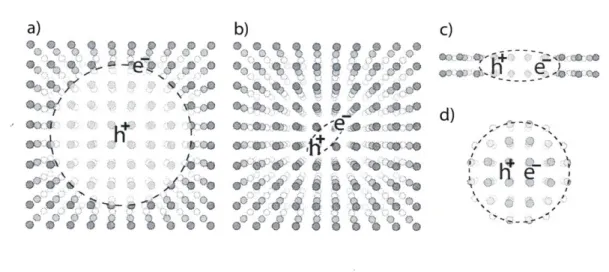
d)-Figure 2-1: Exciton varieties. (a) Bulk Wannier-Mott exciton (b) Bulk Frenkel ex-citon (c) An exex-citon confined in one dimension (d) An exex-citon confined in three dimensions
In materials with appreciable permittivities such as bulk inorganic semiconduc-tors (e.g. silicon, germanium, III-V semiconductors, metal oxides), the electron-hole Coulomb interaction is well screened and the binding energy is relatively small
(Ex < 100 meV). Such excitons, called Wannier-Mott excitons have large spatial
extent (~ 5 - 10 nm) and behave analogously to a hydrogen atom composed of
charges with reduced effective mass and with a strongly screened Coulomb interac-tion. Consequently, the exciton binding energy is much smaller than the hydrogen atom ionization energy. Some semiconductors exhibit a progression of excitonic states analogous to the electronic energy levels of a hydrogen atom, which can be observed using absorption spectroscopy at low temperature [38]. A Wannier-Mott exciton is illustrated in Fig. 2.1.1a.
In materials with small permittivities (such as polymer solids, organic crystals, and inorganic crystalline insulators) photoexcited electrons remain strongly correlated with the hole from which the electron originates. The Coulomb attraction is poorly screened and the exciton binding energy can consequently be quite large (Ex ~ 0.1-1 eV). In this regime, the exciton is highly localized; the bound exciton radius is less than a nanometer and often less than the crystal lattice constant. This type of exciton is called a Frenkel exciton, which is illustrated in Fig. 2.1.1b.
In nanostructured semiconductors, it is possible induce prominent electron hole interactions by spatially confining photoexcited charges. Monolayer transition metal dichalcogenides for instance have exciton binding energies on the order of 200-400 meV [39-41]. This is much larger than one might expect based on the bulk materials' large permittivities [42]. The surprisingly large binding energy is caused by inefficient screening in atomically thin materials. Though the material itself is highly polariz-able, the surrounding medium usually is not. Consequently, charges can still interact strongly by bypassing the polarizable medium in favor of the surrounding dielectric.
This idea is illustrated in Fig. 2.1.1c.
In spherical nanocrystals, electron-hole interactions are forced by confining the charges in all three dimensions. Though it can be difficult to decouple the size-dependent valence and conduction band edge from the size-size-dependent exciton binding energy in quantum dots, Meulenberg et al. measured the band alignments using X-ray absorption and photoelectron spectroscopy [43j. They found that the exciton binding energy in CdSe quantum dots ranged from 0.2 - 1 eV, which is much larger than the binding energy in bulk CdSe (15 meV) due to confinement of the electron and hole to the same region. This motif is illustrated in Fig. 2.1.1d.
The strength of a material's light-matter interaction with respect to a given tran-sition g -+ e is governed by the magnitude of the transition dipole moment, which
is mediated by the excited and ground state wavefunction overlap: Peg = (V'eIqr|,,).
Strongly bound excitons typically possess large transition dipole moments and appear in semiconductor absorption spectra as narrow features red shifted from the electronic band gap by the exciton binding energy. Similarly, excitons can emit, but this process occurs in competition with thermal exciton dissociation.
2.1.2
Transition Metal Dichalcogenides Background
Electronic properties of TMDs: In 2010, Mak et al. isolated atomically thin MoS2
[201, building upon the Nobel Prize winning isolation of graphene in 2004 [44j and expanding the field of two dimensional (2D) crystalline materials to include transi-tion metal dichalcogenides (TMDs). Similar to graphene, TMDs exhibit high carrier