- I
A Comparative Study of High Voltage Analog
i*'I4M
Switch Topologies
by
Angela N. Odongo
S.B. EE, M.I.T., 2013
Submitted to the Department of Electrical Engineering and Computer
Science
in partial fulfillment of the requirements for the degree of
Master of Engineering in Electrical Engineering and Computer Science
at the
MASSACHUSETTS INSTITUTE OF TECHNOLOGY
June 2014
@
Massachusetts Institute of Technology 2014. All rights reserved.
Signature redacted
A uthor ...
Department of Electrical Engineering and Computer Science
Certified by...
Signature redacted
May 23, 2014
Certified by...
Adam Shou
Design Engineer, Linear Technology Corporation
Thesis Supervisor
Signature redacted
/...
-
. ...
David J. Perreault
Professor of Electrical Engineering
Signature redacted
Thesis Supervisor
A ccepted by ...
Prof. Albert R. Meyer
Chairman, Masters of Engineering Thesis committee
MASSACHUSETTS INGimJTE OF TECHNOLOGY
JUL
15
2014
LIBRARIES
A Comparative Study of High Voltage Analog Switch
Topologies
by
Angela N. Odongo
Submitted to the Department of Electrical Engineering and Computer Science on May 23, 2014, in partial fulfillment of the
requirements for the degree of
Master of Engineering in Electrical Engineering and Computer Science
Abstract
The design of electrical switches continues to develop as the demand on performance specifications increases and device fabrication processes improve. They have applica-tion in automated test equipment, variable gain feedback amplifiers, sample and hold circuits, and other switched capacitor circuits. In this document, four high voltage analog instrumentation switches were designed using different topologies. The four switches were then compared with respect to various important switch performance characteristics.
Thesis Supervisor: Adam Shou
Title: Design Engineer, Linear Technology Corporation Thesis Supervisor: David J. Perreault
Acknowledgments
I would like to express my gratitude to Linear Technology for giving me the
oppor-tunity to work with their excellent engineers on this project. This project would not
have been completed without the help, training, and patient teaching of my thesis
supervisor at Linear Technology, Adam Shou. I would also like to thank Brian
Hamil-ton, for guiding me, keeping the project on track, and for making me start writing
up this document early enough.
I would also like to thank Professor David Perreault, my MIT thesis supervisor
for making sure my project stayed on track, and for reviewing this document. My
thanks go to the EECS department at MIT for the VI-A program.
My gratitude also goes to Tyler Hutchison and John Fiorenza for their help and
encouragement through the process. The car talks will always be remembered fondly.
Thilani and Wendi, your guidance was invaluable. Eko, thank you for making me get
my driver's license.
On a more personal note, I would like to express my sincere gratitude to my
family for always encouraging me through the toughest of times. I thank God for the
opportunities He has given me, and for giving me the support of a loving family to
take on challenges, even from thousands of miles away. For the family that's closer
to MIT, thank you for looking out for me.
And for all the wonderful people I have had the pleasure of meeting during my
time at this great Institute, I am grateful. I was blessed to have an ever supportive
academic advisor, Jing Kong, who took the time to make sure I stayed on the path
towards a fruitful and successful semester, every semester. For all the friends, and
my fellow course 6-1 students, thank you for the fun times that we had on this wild
Contents
1 Introduction 13
1.1 Thesis organization . . . . 14
1.2 Devices used . . . . 14
2 Topologies and operation 17 2.1 Drain coupled switch . . . . 18
2.2 Drain coupled switch v2 . . . . 19
2.3 Source coupled switch . . . . 20
2.4 Source coupled switch v2 . . . . 21
3 DC Characteristics 23 3.1 On Resistance . . . . 23
3.2 Leakage current . . . . 25
3.2.1 On Leakage . . . . 26
3.2.2 Off Leakage . . . . 28
3.3 Short circuit protection . . . . 29
3.3.1 Drain coupled switch VGS generator . . . . 30
3.3.2 Source coupled switch VGS generator . . . . 32
4 Charge Conservation 37 4.1 Diode ... ... 38
4.2 Vertical PNP .. ... .. . . . .. . . . .... .. . .. .. .. 41
4.3 Maxer circuit ... ... 43
5 Charge injection 47
5.1 Drain coupled switch turn off . . . . 49
5.2 Drain coupled switch turn on . . . . 50
5.3 Source coupled switch turn off . . . . 53
5.4 Source coupled switch turn on . . . . 54
6 Robustness and Protection 57 6.1 Drain coupled switch . . . . 57
6.2 Source coupled switch . . . . 62
7 Tests and Comparison. 63 7.1 On resistance . . . . 64
7.2 Leakage current . . . . 66
7.2.1 On leakage . . . . 68
7.2.2 Off leakage . . . . 69
7.3 Charge conservation . . . . 69
7.4 Charge vs step size . . . . 73
7.5 Charge injection . . . . 76 7.6 Insertion loss . . . . 78 7.7 Off Isolation . . . . 79 7.8 Overall comparison . . . . 81 7.9 Conclusion . . . . 81 7.10 Future work . . . . 81 7.10.1 VGS generators . . . . 81
7.10.2 Alternative slew boost . . . . 82
7.10.3 Multiplexer . . . . 84
List of Figures
1-1 Cross section of lateral HVPMOS device . . . .
2-1 Single HVPMOS switch ...
2-2 Simplified drain coupled switch topology . . . .
2-3 Simplified drain coupled switch topology, version 2
2-4 Simplified source coupled switch topology . . . .
2-5 Simplified source coupled switch topology, v2 . . . .
On resistance vs VSG . . . .
On leakage diodes . . . .
Off leakage diodes . . . . SC1 short circuit test . . . .
Simplified VGS generator for drain c
3-6 Simplified VGS generator for SC1
Simplified SC2 short circuit model
Source coupled switch current limitir
. . . . 24
. . . . 27
. . . . 28
. . . . 29
oupled switch topology . . . . . 31
. . . . 32 . . . . 33 g VGS generator. . . . . 34 Input charge . . . . Source follower . . . . Feed-forward capacitor . . . . HVPMOS vertical PNP data . . . . . Maxer circuit schematic . . . . Three input maxer circuit schematic . . 38 39 . 40 42 44 45 5-1 Charge injection test . . . . . . . . 47 15 . 17 . 18 . 19 . 20 . 21 3-1 3-2 3-3 3-4 3-5 3-7 3-8 4-1 4-2 4-3 4-4 4-5 4-6
5-2 Charge injection capacitive coupling
5-3 Maxer with comparator . . . . 52
5-4 Latch for DC2 turn on control. . . . . 52
5-5 Three way maxer comparator . . . . 54
5-6 Turn on latch . . . . 55
6-1 VGS clamp . . . . 59
6-2 Extra drain pull down and gate pull up currents . . . . 62
7-1 General switch symbol . . . . 63
7-2 Large signal on resistance test . . . . 64
7-3 Large signal on resistance . . . . 65
7-4 Small signal on resistance test. . . . . 66
7-5 Small signal on resistance over temperature test. . . . . 67
7-6 Off leakage current test setup. . . . . 68
7-7 On leakage diodes . . . . 68
7-8 On leakage current over temperature test . . . . 70
7-9 Off leakage diodes . . . . 71
7-10 Off leakage current over temperature test . . . . 72
7-11 Charge conservation test setup setup. . . . . 73
7-12 Charge conservation at rising slew . . . . 74
7-13 Charge conservation at falling slew . . . . 75
7-14 Charge vs step size . . . . 77
7-15 Turn off charge injection. . . . . 78
7-16 Bandwidth . . . . 79
7-17 Isolation . . . . 80
7-18 CTAT current source. . . . . 83
7-19 Alternative feed-forward. . . . . 84
A-1 Vertical PNP behavioral model . . . . 88
List of Tables
1.1 Table showing main transistors used in this project . . . . 15
2.1 Expected size comparison . . . . 21
3.1 VGS generator comparison . . . . 35
6.1 On-state protection cases in DC2. . . . . 58
6.2 Off-state protection cases in DC2 . . . . 61
Chapter 1
Introduction
High voltage analog switches have application in many fields, for example in medical
devices like ultrasounds, motor drive, power conversion and switched-mode power
supplies, and in automotive applications. They are also important in automated test
equipment (ATE) setups where it is important to be able to electrically control the
turn on and off behavior of the switches used. All characteristics of the switch that
affect the accuracy of the ATE measurements have to be taken into consideration.
The main difference between low voltage and high voltage switches is the range
of voltages that can be applied between the terminals of the switch. Low voltage
normally applies to up to 15V. The 150 volt switches discussed in this project can
take up to 150V between the two terminals T1 and T2, allowing a wide swing in
signal voltage.
There are two types of high voltage switches: power switches and
instrumenta-tion switches. Power switches are designed to carry large currents, therefore very
low on resistance, wide robust operating region, and good thermal behavior are the
most essential electrical characteristics. On the other hand, instrumentation switches
usually carry lower current, which leads to a requirement of relatively constant on
resistance over a wide range of currents, low charge injection, and very low leakage
current, which would lead to voltage offset, especially when used in current sensing
applications.
which provides bipolar, CMOS and DMOS (double diffused MOS) devices. However, using a non SOI process means that the parasitic devices, which could lead to latch up risks, have to be taken into account.
1.1
Thesis organization
Since the purpose of this project is a comparison of switch topologies, each chapter will cover a different aspect of the switch design, explain the concept, quantify the specification and perform a comparison of the expected behavior of each topology. Additional circuitry may be added to improve performance.
Chapter one introduces the topologies, and later chapters will cover important electrical characteristics for each switch topology, gradually increasing the function-ality and complexity of the switch from the simplest form to a complete system. Finally, tests will be performed side-by-side for a complete comparison of all four topologies.
1.2
Devices used
The high voltage PMOS (HVPMOS) devices are double diffused drain MOSFETs with a lightly doped drain profile. The spacing between the drain contact and the gate is long so that it can allow up to 150V between drain and source. These devices are large and take up a lot of space on the die because of the large spacing required for junction isolation between the drain and the body, and between the body and the substrate. They were used mainly in the input signal path and as high voltage cascode devices in the switch control circuitry. Figure 1-1 shows a simplified cross section of the HVPMOS device used in this project.
The P- region beside the drain is known as the drain extension area and takes over the blocking voltage. These devices have the disadvantage of a low current-load capacity because the P- area demands a large part of the surface of the semiconductor.
Source
Gate
o4~Drain
I-A
Il-N-epi
Buried N Layer
4
P Substrate
Figure 1-1: Cross section of lateral HVPMOS device
Other low voltage MOSFETs are also used in this project. These devices are
smaller and offer good device matching.[6] They are also more accurate because of
better parameter control in the process, and thus were used for more accurate current
mirrors and low voltage comparators.
Table 1.1 below summarizes the main transistors used in the design and schematics
shown in this document, and their maximum operating voltages. The extended drains
of the HVPMOS and HVNMOS are indicated on the symbol with three diagonal lines
for easy recognition.
Transistor Symbol VDS max VGS max VBS max
HVPMOS
150
15
13
LV PMOS
5
5
5
HVNMOS
150
15
0
LV NMOS
5
5
5
Table 1.1: Table showing main transistors used in this project
15
K-Chapter 2
Topologies and operation
A simple switch topology would use a single high voltage MOSFET between the
switch terminals. For example, with a single HVPMOS device, as shown in figure 2-1
below, with the drain-body and source-body diodes explicitly shown.
Figure 2-1: Single HVPMOS switch
This switch would only work for unipolar application, i.e one voltage is known to
be always higher than the other. If the body and the source are tied together, the
drain-body diode would be forward biased when the source voltage falls below that
at the drain. Additionally, this single MOSFET switch would carry some part of any
AC signal via the drain-body diode, even when the switch is off.
Since the HVPMOS devices in this process are not symmetric, the body-source
breakdown voltage is much lower than that at the body-drain junction. Thus two
PMOS devices were used in series between the switch terminals, enabling design
of symmetric bi-directional switches without this restriction, enabling the switch to
stand 150V in either direction. This also adds a middle node which allows more
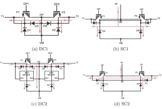
For this project, two main topologies are covered; drain coupled, and source
cou-pled switch topologies, which both provide a symmetric bi-directional switch. They
differ by which of the HVPMOS nodes are connected together.
2.1
Drain coupled switch
The first drain coupled switch topology (DC1) uses two HVPMOS devices connected
at their drains. A simplified version of the topology is shown below. Devices P1 and
P2 are 150V HVPMOS transistors, and their shared drain node is labeled DP. Their
gates will be referred to as GP1 and GP2 respectively.
N N Ggen C4 VGS
T14 T2
PI P2 IPD
Figure 2-2: Simplified drain coupled switch topology
The VGS generators shown in the schematic control the gate drive voltages for P1
and P2 depending on the external control voltage "ON" which signals for the switch
turn on/off behavior. For the switch to be turned off (open), pin ON is pulled low
(VM) and for the switch to be on (closed), it's pulled high (VM + 5V). Since P1
and P2 have independent source and gate voltages, two separate (but identical) VGS
generators are required. When the "ON" signal is high, both VGS generators turn
on P1 and P2, creating a low resistance channel path from T1 to T2.
When the switch is on and operating normally (low load current), the voltages at
T1, DP, and T2 are approximately equal, and with a VSG of about 5V, both P1 and
P2 are in triode mode of operation, behaving like linear resistors.
For switch turn off, node DP is pulled down to VM by current IPD to ensure that
T1 and T2.
This topology has limitations due to leakage current and the fact that the maxi-mum voltage across the terminals has to be limited to prevent turn on of the vertical PNP parasitic device that is part of the HVPMOS structure.
For the purpose of this study, the node labeled T1 was considered the input side and T2 the output, where the input is connected to a voltage source, and the output to the load.
2.2
Drain coupled switch v2
Figure 2-3 below shows a simplified schematic of the second drain coupled switch topology, DC2.
N ONG[g"n VGS eON ON
T1 DP _T2
INMAXEIN2 IN2 NM
11PD
Figure 2-3: Simplified drain coupled switch topology, version 2
Similar to DC1, this topology uses two HVPMOS devices connected at the drain. However, the body ties for P1 and P2 are changed to give a new topology, DC2. The body is biased to the higher of the drain and source voltage of P1 (and P2) by a maxer circuit. The behavior of a two input maxer is simply described by equation 2.1.
V(OUT) = max(V(IN1), V(IN2)) (2.1)
devices P1 and P2, and the maxer gave the higher voltage as output which was used to bias the body, ensuring that the parasitic vertical PNPs associated with the HVPMOS device structures can be kept off. P1 and P2 each require their own maxer circuit for their body. The maxer has a MOS gate at each input, thus it does not require input current that would be taken from the main signal path. The maxer circuit and other reasons/advantages for using a maxer will be discussed in section 4.3.
2.3
Source coupled switch
In contrast to the drain coupled topologies, this source coupled switch (SCI) uses the two HVPMOS devices connected at their sources. A simplified version of the switch topology is shown below. Similar to the drain coupled version, devices P1 and P2 are 150V PMOS transistors, and their shared source node is labelled SP. Since P1 and P2 share a source, with their gates connected (node GP), only one VGS generator is required.
The main operation of this topology is similar to that of the drain coupled switches previously described. However, for switch turn off, current IpU is used to pull up the middle node SP to VP voltage, ensuring that the body diodes of P1 and P2 are reverse biased when the switch is off.
VP
11PU
T1 P1 T2
VGS ON ON
2.4
Source coupled switch v2
The source coupled switch can also be implemented using a maxer for the body tie of the common bodies of P1 and P2 as shown below. This gives the fourth and final switch topology, SC2. Given the cormnon body node, this topology can be implemented with one three-input maxer whose output is the highest of the T1, T2 and SP voltages.
V(OUT)
=
max(V(IN1), V(IN2), V(IN3))
(2.2) This maxer ensures correct body bias even during the switch turn off transient as the source is pulled up to VP.VP IPU 1N2 INi MAXER P1 OUT IN3 P2 TI n- T2 VGS n ON ON
T
Figure 2-5: Simplified source coupled switch topology, v2
Given the topologies introduced above, some comparison points can already be
noted.
DC1 DC2 SCi
SC2
Number of VGS generators 2 2 1 1
Number of maxers 0 2 0 1
Table 2.1: Expected size comparison
From this, it can be expected that switch topology DC2 would have the largest die size when fabricated in silicon, and SCi the smallest. Depending on the imple-mentation of the VGS generators and maxers, the relative sizes will determine the
final size of the switch topologies. This is an important point to note since die size directly defines the cost of the final integrated circuit.
Chapter 3
DC Characteristics
This chapter deals with the DC characteristics of previously introduced switch
topolo-gies DC1, DC2, SCI, and SC2, namely; on resistance, on and off leakage current, and
short circuit current. These are very important characteristics in a switch. [5]
3.1
On Resistance
For a switch to more closely approximate ideal behavior, it is desired that the on
resistance is minimized, reducing the voltage drop across the switch when closed.
As previously mentioned, the HVPMOS features a lightly doped extended drain
which enables it to carry the full current when "on", and block high voltages when
"off" .
Total switch on resistance is a sum of the channel resistance Rch and the resistance
due to the drain extension, Rdd.
For a MOSFET in triode, the source-to-drain current is given by:
IWC(
V
DS(31 IDS ~~ -TloxkGS -th - )VDS (3.1)L 2
Assuming that the VDS is small when the switch is in triode, we can assume that
L
1
1
Rch = -- - - 1(-2
W pCox (VGS - Vth)
From this, it can be seen that the channel resistance is proportional to
y
wand
inversely proportional to the gate overdrive voltage. Assuming that the gate overdrive
voltage will be approximately the same for P1 and P2 in a given switch topology,
then the channel resistance will depend only on the l ratio of P1 and P2. Thus for
La fairer comparison between topologies, P1 and P2 have the same length and width
in all topologies considered in this project.
Figure 3-1 below shows the dependence of on resistance of a single HVPMOS
device on the gate-source voltage. The device used in this test has the same
Wratio
as P1 and P2 in the switch topologies.
Plot of on resistance vs VSG
E
(0 o
Figure 3-1: On resistance vs VSG
From figure 3-1, it can be seen that the dependence of on resistance on gate
overdrive voltage is greatly reduced at a VSG greater than 4V. The extended drain is
then the main factor in the on resistance of the switch, and is the limiting factor in
the total resistance. In order to have control over the switch resistance for current
limiting purposes, a VSG was chosen such that Rch was about 10% of the total switch
RON.
material, and the length of the drain extension region, Ldd.
w
Rddoc
(3.3)
Ldd
Given that Ldd is fixed in the device process, Rd can only be altered by changing the width of the device. Given the measurements in figure 3-1, the drain resistance can be approximated to be about 80Q.
Given the strong dependence of switch on resistances Reh and Rd on the width of the device, the same width was used in devices P1 and P2 in all switch topologies, in order for them to all have a approximately the same on resistance.
Total switch resistance is also known to be related to the breakdown voltage, VB
of the device, that partly determines the voltage rating of the device. [1]
RDS(ON) C .6(
The high voltage rating of the HVPMOS devices explains the relatively high on resistance of these switches.
This figure only shows the range of VSG values when the switch is sufficiently turned on. Not shown in the figure is the 165Mg resistance at VSG below 0.3V. Thus for switch turn off, VSG was set to -1V to ensure behavior close to ideal.
3.2
Leakage current
Leakage current is an important DC characteristic of a switch because of the loss of current and the voltage offset it causes. It is desirable to minimize the switch leakage current in both on and off states of the switch.
The main causes of leakage in the switches are the reverse biased diodes in the main switch path. At low reverse bias voltage, diode current is approximately independent of voltage, but increases with temperature. However, at a reverse bias greater than a few k, the diode reverse current is given by [7]
q
irev = Aqni W(v) (3.5) 27-0
where A is the area of the junction, ni is the intrinsic carrier concentration, To
is the carrier lifetime in the depletion region, and w is the width of the depletion
region, which depends on the applied reverse bias voltage, v. The intrinsic carrier concentration ni depends on temperature as shown in the equation below:
3
ni
oc T2 (3.6)It is thus expected that the leakage current of diodes in the HVPMOS devices will increase with size, temperature, and reverse bias voltage.
In the following sections, expected leakage current will be discussed with the aid of schematics of main switch path devices, explicitly showing the diodes. Actual behavior will depend on the implementation of all parts of the switch design and will be revisited and further discussed later.
3.2.1
On Leakage
When the switch is on and functioning normally in DC conditions, with low load current, it is expected that for the drain coupled switch, T1, DP and T2 will be at approximately the same voltage. And similarly for the source coupled switch, T1, SP and T2 voltages are expected to be very close.
Figure 3-2 below explicitly shows the diodes in the main switch path that
con-tribute to the leakage current when the switch is on. The pull up and pull down current sources have cascode devices that add high voltage drain-body diodes, which also contribute to leakage current and have thus also been included for each topology. Since the switch is on, the terminals and middle nodes (DP or SP) are expected to be at about the same voltage. Thus the drain-body and source-body diodes of P1 and P2 in all topologies are essentially shorted out and are not explicitly shown in
figure 3-2.
GP1 P1 T1 -D1 VI (a) DC1 GPI G 2 T1 P1 D P2 T2 ) Y BY M.ER ER
IN1 IN . IN1 IN2
it 3 D2 VA (c) DC2 GP2 GP 05 T2 P P2 T2 D3 D4 VM (b) SC1 VP
051
TP P TT SP N2 T2 VM (d) SC2Figure 3-2: On leakage diodes
to the expectation that leakage current will increase with increasing voltage at the
terminals T1 and T2 as this increases the reverse bias voltage across D1, D2 and D5.
Similarly, for DC2, D1, D2 and D3 are reverse biased. However, D1 and D2
currents are sourced by the maxer, and do not contribute to the leakage current
measured at the terminals. As T1 voltage increases, the reverse bias on D3 increases
as well, and as such, the leakage current is expected to increase with terminal voltage.
Less on leakage current is expected in DC2 than in DC1.
For SC1, D3, D4 and D5 are expected to be the main causes of leakage current.
D5 leakage current can provide the leakage current to D3 and D4 from VP, and any
extra (/deficit) current flows to (/from) the terminals and is measured as leakage.
Thus for SC1, it is expected that leakage current will increase with terminal voltage,
crossing the point of zero leakage when D5 current is exactly equal to the sum of D3
and D4 currents.
With the maxer in SC2, D3 and D4 currents are provided by the maxer and D5 is
expected to be the main cause of leakage current, whose magnitude is thus expected
to decrease with terminal voltage, to a final value of 0 when D5 has 0 volts across it.
27
GP1 G 2 VP
T
GP GP (a)DP P2 (b S I T1 T T2 6SP D3D4 N D1 D2 D3 D4Ak VM VM (a) DC1 (b) SC2 GPI GP2 T32 A __ DL T2 VP D b ? D5 I I2 INMB EIN2 T1T1P D1D2 D1 D3 D 2 \M VM (c) DC2 (d) SC2Figure 3-3: Off leakage diodes
3.2.2
Off Leakage
Off leakage depends on the behavior of the diodes shown in figure 3-3.
When a drain coupled switch is tuned off, the common drain node DP is pulled
down to VM. For DC1, the measured leakage current will thus depend on diodes D1,
D2, D3 and D4, and is expected to increase with increasing terminal voltage.
For DC2, reverse leakage current is supplied by the maxers. Only D4 and D5
currents are measured at the terminals. Since the maxers hold the bodies of P1 and
P2 close to their respective source/terminal voltages, D4 and D5 have only a small
reverse voltage across them. Thus the leakage current measured at the terminals is
expected to be small and approximately constant for DC2 in off state, over the range
of TI voltages.
For turn off of the two source coupled topologies, the sources and bodies of P1 and
P2 are pulled up to VP, thus the maxer is not needed and is not shown in figure 3-3.
As a result, the same diodes, Dl and D2, determine leakage current in both SCi
and SC2 topologies. Their reverse bias voltage reduces as terminal voltage increases,
leading to reduced leakage current measured at the terminals.
3.3
Short circuit protection
It is desirable that the switches are protected in the event of a short circuit. Take for example SCI, which is replicated below.
VP
PU
P1 P2
VGS nON ON
Figure 3-4: SC1 short circuit test
If T2 is tied to ground, and T1 voltage is slowly increased, then at low voltages, P1 and P2 are in triode and behave like resistors, and the voltage divides equally between the two devices. Assuming a body diode forward voltage of 0.7V, when T1 voltage reaches 1.4V, the body diode of P1 will be turned on, turning on its parasitic vertical PNP device. As T1 voltage is further increased, the voltage across P1 does not increase and most of the drop falls across P2, and the switch no longer behaves
resistively. Thus in order to prevent this from happening in SC1, assuming an RON
of 200Q the maximum current that the switch should carry is 7mA as derived below:
O.7V
_0.7_I OW--
100
= 7mA (3.7)2
Similarly for DC1, if T1 voltage is increased as T2 is tied to ground, when T1
reaches about 1.4V, the drain-body diode on P2 clamps its VDS to 0.7V and as T1 is
further increased, extra voltage falls across P1 while that across P2 is fixed.
However, the switches with maxers for body bias (DC2 and SC2) can go to much higher voltage difference between terminals without turn on of the vertical PNP of
P1 or P2. If the maximum VBS is clamped at 7V by the maxer, this would give a 10x
increase in the range of differential voltage in which switch behavior is resistive. In the case that the switch is forced into a short circuit condition, with a large
voltage applied between its terminals, it is important to protect the main switch
HVPMOS devices P1 and P2 from damage. A short circuit current limit was chosen
to prevent the body diode (and parasitic vertical PNP) from turning on in such a DC condition.
Different mechanisms may be used to limit the short circuit current. For the four topologies, these mechanisms were implemented within the VGS generator scheme, reducing the VSG in order to reduce the current that the switch will carry. The following subsections will introduce the VGS generator schemes used in each switch topology.
3.3.1
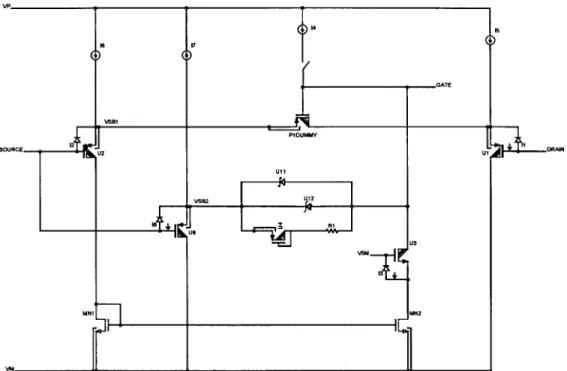
Drain coupled switch VGS generator
As previously mentioned, the VGS generator controls the turn on and turn off behav-ior of the switch, as well as the short circuit current limiting. For the drain coupled topologies, current limiting is implemented by reducing the gate overdrive voltage on P1 or P2 when a short circuit condition is sensed.
A simplified schematic of the VGS generator used for the drain coupled switch
topology is shown in figure 3-5 below.
The main switch HVPMOS devices, P1 and P2 each require a separate VGS generator in the drain coupled switch topologies. For each device, the source, gate and drain would be connected to the appropriately labeled terminals of the VGS generator.
When the switch is on and operating normally (low load current), the gate drive is generated by the voltage drop across resistor R1. The maximum VSG is clamped
by the zener diode, U12. Since node VSB2 is the buffered source voltage from P1,
the gate voltage generated will be referenced to the source as required.
For switch turn off, current source 14 is connected and the Schottky diode U11 is forward biased. The Schottky forward voltage drop, in addition to the VSG of the source follower device U9, ensure that the VSG of P1 is negative, ensuring complete
turn off of the HVPMOS.
VS411
I 17
SOVRCE U DRN
U1U1
MN1 MN2
Figure 3-5: Simplified VGS generator for drain coupled switch topology
step up of the VSG of the source follower has to be compensated for. This could be
done by increasing the resistor size, but use of the diode connected HVPMOS device,
U4 ensures that the source follower VSG is better canceled out over temperature and
process variations.
In the case of a short circuit condition, if for example T1 is pulled up to VP
and T2 is shorted to ground, most of the voltage drop occurs across P1, putting P1
in saturation and leaving P2 in triode, and the switch carries a large current. The
strategy used to limit the current in this topology is to reduce the gate overdrive
voltage on P1 to a value that limits the current to a known and acceptable amount.
The short circuit condition is sensed by replicating the gate, drain, and source voltages
of P1 onto PIDUMMY (in the VGS generator), an HVPMOS similar to P1. Thus
the current through P1DUMMY is representative of the P1 current. The - ratio ofL
PIDUMMY is scaled from that of P1 so that less current can be used in the VGS
generator during current limiting, saving on power consumption. This also saves some
space on the die since P1 and P2 have large width W to minimize on resistance.
sensed current, the loop stability was tested using Middlebrooks Null Double Injection Method [4], breaking the loop at the drain of device MN1. Using this method, the loop was found to be stable. Stability was also tested under different load, source and temperature conditions and the results showed loop stability in all the tested conditions.
The same VGS generator was used for both drain coupled switch versions; DC1 and DC2.
3.3.2
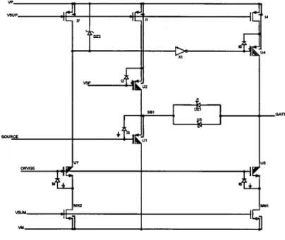
Source coupled switch VGS generator
For SC1, a simple VGS generator with Zener and Schottky diodes for turn on and turn off mechanisms was implemented, as shown in figure 3-6 below.
VP V5UP 1 17 , IDZ n 1 X1 w SOURC MN2 MNI
Figure 3-6: Simplified VGS generator for SC1
The main input to this VGS generator is the source voltage, which is buffered by HVPMOS Ul source follower. The output gate voltage used to drive the shared gate, node GP. The VGS generator turn on/off is controlled by node ONVGS, which goes up to VM + 5V, and for turn off, it goes to VM.
The Zener diode DZ1 is reverse biased to give a 5V VGS for switch turn on. For switch turn off, a small current from device 14 is used to pull the gate voltage above
the source, forward biasing the Schottky diode. The low Schottky forward voltage, in addition to the VG of the source follower creates a negative source-gate voltage, to ensure that P1 and P2 are completely off.
This VGS generator implements turn on and turn off of the switch, but does not include any short circuit current limiting. This adds to the advantage of SCi in simplicity and die space savings. It also aids in the comparison of topologies by enabling any shortcomings or advantages of the simplicity of this VGS generator scheme to be shown clearly in the final comparison.
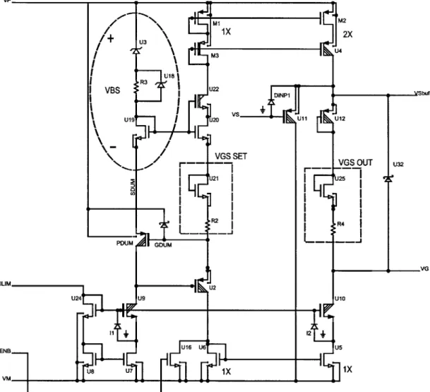
For switch topology SC2, with the maxer, a different VGS generator scheme was used to take advantage of the body bias scheme to incorporate short circuit protection. In the case of a short circuit, if for example TI is tied to VP and T2 is grounded, most of the voltage drop falls across P2, pushing P2 into saturation while P1 remains in triode. With the maxer, the bodies of P1 and P2 are essentially both connected to T1 voltage, which will be higher than T2. This creates a separation in the body and source voltages for P2. Simplifying P1 as a resistor, the main switch devices can be viewed as in figure 3-7.
1
R1 T2 RDSON T V(VP)Figure 3-7: Simplified SC2 short circuit model
From this representation, it can be seen that as the switch current increases, the source-body separation for P2 increases, and by the body modulation effect, P2's threshold voltage is increased, reducing the effective gate overdrive voltage and thus the drain-source current in the switch main devices P1 and P2. This topology thus has self-protecting behavior for short circuit conditions.
con-dition above is replicated in the VGS generator, as shown in figure 3-8 below, using scaled down dummy devices, a scaled amount of the short circuit current limit, and the maximum targeted body and source separation voltage. This VGS generator then creates a constant VGS that would limit the maximum switch current to 30mA, i.e a constant VGS of about 3.5V. VP ..
M1 I
U3 M3 RU181 VBS R3 U19 U20 -/ VGS SET 21 R2 PDUM GDUM U2719
2i 2 ENB U16 U6 U VMU8 U7 1X M2 2X -U4 DINPI U11 U12 VGS UT U25 R4 U110 1XFigure 3-8: Source coupled switch current limiting VGS generator.
Current ILIM shown in figure 3-8 is a scaled amount of the current limit and is drawn through a HVPMOS device PDUM, which is a scaled version of the main HVPMOS devices in the main switch path, P1 and P2. The VBS set by the circled devices is the chosen maximum VBS of 7V. The VGS of PDUM is therefore the VGS that would enables PDUM to carry current ILIM, as is shown as VGS SET in the
.. M Sbuf U32 L I VG ILIM U24 I I
dashed square. This voltage is then copied to VGS OUT, referencing it to the source voltage VS. The outputs of this VGS generator are thus VSbuf, a buffered copy of the source voltage, and VG, the gate drive voltage.
The table below summarizes the comparison of the DC characteristics discussed in this chapter. Since it is difficult to summarize the expected leakage current behavior, the table will only include expected on resistance and a comparison of the VGS
generators designed. The simplicity of the VGS generator circuit is expected to
correspond with the size of the circuit, especially where many HVPMOS devices are needed. The VGS generators can also be compared by whether each has current limiting capabilities. The current limits were all set to 30mA as previously described.
DC1 DC2 SCI SC2
RON (Q) 200 200 200 200
Simple VGS generator circuit / / / x
Current limiting / / x /
Table 3.1: VGS generator comparison
Given that the P1 and P2 devices in each topology have the same W, they are all expected to have a total on resistance, between terminals TI and T2, of about 200Q. The drain coupled topologies have both simplicity and current limiting abilities, whereas both of the source coupled versions have one or the other.
Chapter 4
Charge Conservation
An ideal switch passes all charge from the input to the output. In this study, charge
conservation refers to maintenance of the same input charge required by the switch
over a wide range of slew rates, for a fixed input voltage step size. Charge conservation
is a key design parameter for an instrumentation switch and is an important focus of
study in this document, because charge loss leads to a voltage offset. Charge loss that
is linear with input step size is tolerable in most applications as it causes a constant
gain error that can be fixed by calibration, whereas non-linear gain error is not easily
calibrated out.
The ideal input charge vs slew rate plot would be flat up to 1000V/Ps, as shown in
figure 4-1. This requires that even as the input slew rate increases, no extra charge is
taken from the signal path and lost in the switch's internal capacitances. The figure
also shows the measured behavior from switch topology SC1, which does not include
a maxer circuit.
The main sources of charge loss in all the switch topologies are:
* The protection diodes at fast slewing nodes which may be momentarily forward
biased during a slew transient.
" Turn on of the parasitic vertical PNP device that is part of the isolated high
voltage PMOS devices used in the main switch.
SC1 input charge X10 -Simulated 325 - --Ideal 3.15-341 2) 3.00 0)3 2.95- 2.9-2.85 0 100 200 300 400 500 600 700 000 900 1000
Slew Rate (V/jis)
Figure 4-1: Input charge
4.1
Diode
A protection diode was used from gate to source on HVPMOS source followers and
on HVPMOS cascode devices, as shown in figure 4-2, to prevent the gate voltage from
being pulled more than a diode drop above the source voltage, as shown in the figure.
If the input to a source follower (VIN) is connected to T1 during fast rising slew, and
its output is capacitively loaded, the gate of the HVPMOS U1 may be pulled more
than 5V above the source during slew, leading to gate oxide breakdown. By having
the diode between the gate and source, the source follower input directly charges the
load capacitance, pulling up the source of U1.
This diode therefore leads to charge loss when the source follower input is
con-nected to any of the nodes on the main signal path. If the diode is forward biased
during fast rising slew, a lot of current is directly taken from the main signal path
and used to charge up internal switch capacitances.
Figure 4-2 simplifies the source follower load as a capacitor Coad. The protection
diode is forward biased when all the source current (IS) is being used to charge the
load capacitance. Thus the maximum slew rate, below which the protection diode is
not forward biased, is determined by the current, IS, and the load capacitance.
V M1 IS V5P 12 UU2 VOUT VIN - u1i F 1SF V
Figure 4-2: Source follower
the protection diode on the source follower by ensuring that the protection diodes
are not forward biased during fast rising slew, and that the source followers have a
sufficient gate overdrive voltage and proper behavior is maintained within the range
of slew rates studied.
Method 1: Increasing the DC current to the source follower would keep the
protection diode reverse biased to a higher slew rate. This is however undesirable as
it also leads to an increase in the DC power consumption of the switch.
Method 2: To increase the current only during slew, without increasing DC
power consumption, a feed-forward capacitor is used to provide extra current during
fast rising slew, as shown in figure 4-3 below.
During rising slew of VIN, the capacitor provides current to the cascode device.
U3 stays in cutoff during this transient. The amount of added current is proportional
to the slew rate at VIN. The equations below demonstrate how this feed-forward
capacitor can be used to eliminate the dependence on slew rate.
SR4,, *
Cff +
IS = SRt * Cbmd + ISF (4.1)Assuming: SR,, = SRt = SR:
VP U3 V5P V5P 12 ,U2 VOUT VMN U1 0a 1ISF VM
Figure 4-3: Feed-forward capacitor
Thus by matching the feed-forward capacitor with the load capacitance, the turn on of the protection diode can theoretically be prevented at all slew rates. U1 also gets enough current to prevent collapse of its VSG, maintaining proper source follower behavior.
During fast slew current boost, the cascode device U2 has to carry a lot of extra
current and its VSG may increase transiently. This could force M1 into triode and
significantly reduce the amount of current (IS) it can source. U2 therefore is sized W
with high in order to minimize the variation of its VSG when the slew boost
feed-forward capacitor kicks in.
During falling slew, the feed-forward capacitor sinks current to the input of the source follower. Depending on the slew rate and capacitor size, the feed-forward capacitor may draw more current than the current source provides. This extra current would thus be drawn from forward biasing the protection diode on U2 at fast falling slew. Thus the low voltage NMOS, U3, was added so that the extra current is sourced from the power supply, VP, as shown in the figure. U3 is off at slow slew and turns on just before the cascode device is forced off. The U3 device size depends mainly on the size of the feed-forward capacitor and the amount of current from the current source. The larger the feed-forward capacitor size, the higher the - of U3. The larger theL
w
current source, the smaller the U3
ratio needed.
L
The main trade-off with this method is that it leads to increase in the input
capacitance of the switch.
Method 2, using only a feed-forward capacitor, was chosen due to its simplicity
and easy scalability. Method 1 is not easily scaled to prevent charge loss at fast
slew rates when the source follower is loaded with a large capacitor since that would
mean a large increase in DC power consumption. Additionally, since these protection
diodes are not the biggest source of charge loss, more space and care was taken with
the biggest source of charge loss, which is described in the next section.
4.2
Vertical PNP
The HVPMOS devices P1 and P2 between the terminals T1 and T2 have parasitic
ver-tical PNP devices associated with their layout. The base of the PNP is the HVPMOS
N-type body, the emitter is the P- drain extension, and the collector is the P-type
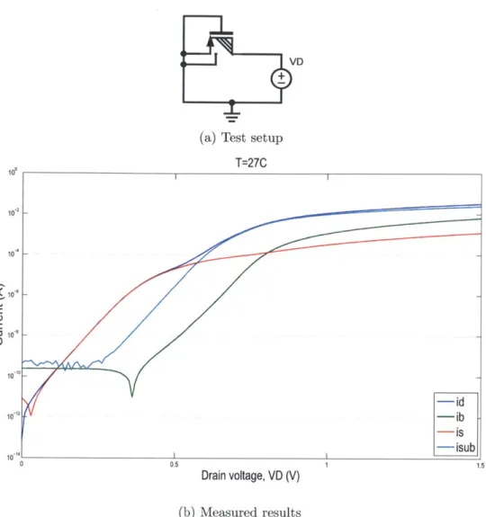
substrate. Measurements of the drain side PNP behavior are shown in figure 4-4.
The test setup shows that gate, body and source were tied together to ensure
that the channel between drain and source was turned off, and the body-source diode
shorted out. This measurement gives data about the drain-side vertical PNP
behav-ior, which is more significant than that of the source-side vertical PNP due to the
relative doping levels of the drain extension and the source.
From the figure, it can be noted that the drain and source currents (id and is) are
equal until a drain voltage of 0.5V. The drain side vertical PNP was measured to have
a high /3 (up to 273 from the measured data) and low turn on V of about 500mV.
This means that this PNP is very easily turned on transiently and will carry a lot of
current to the substrate instead of from T1 to T2 as is ideal for a switch. This parasitic
device is the main cause of charge loss in the switches, taking current directly from
the main signal path to the substrate. Substrate current is also undesirable because
it can lead to latch up issues due to other parasitic devices.
Assuming again that T1 is connected to a voltage source, and T2 is capacitively
..
IVD
....(a) Test setup T=27C -id -ib -is -isub 0.5 1.5 Drain voltage, VD (V) (b) Measured results
Figure 4-4: HVPMOS vertical PNP data
loaded, the input slew rate at which this PNP device is turned on will depend mainly
on the on resistance of the switches and the load capacitance. At a given load
capac-itance, the amount of current required to drive the output at the same slew rate, SR
is given by the product of the capacitance and the slew rate. With that current, and
a known switch on resistance, the slew rate at which the vertical PNP is turned on
is given by:
V=IR
(4.3)
(4.4)
Vbe = Cload *SR
* R,,. 100 102 10 < 10 10' 101c 10 12 10 14 0 1SR
= Vla(4.5)
Cload*
R.n
It can thus be expected that this turn on slew rate will be higher for lower switch on resistance, and lower load capacitance.
The available SPICE model for the HVPMOS device did not include a model for the vertical PNP device to the substrate. However, a behavioral model was made from the measured data shown in figure 4-4, using ideal current sources to model the instantaneous substrate current. The implementation of the model is shown in ap-pendix A. However, this simplified model does not include any dynamic components, like that body-drain capacitance and the body-substrate capacitance, due to their dependence on the device layout in silicon.
The behavioral model of the vertical PNP was added to the main switch devices P1 and P2 in order to see its effect on charge conservation as slew rate is varied. This vertical PNP charge lost to the substrate was found to be the major source of charge loss. Thus it was important to prevent this charge loss by preventing the vertical PNP from turning on transiently. This could be achieved by tying the device body to the higher of the drain or source voltage for P1 and P2. This required the design of a maxer circuit to create the body bias, and that the maxer is fast enough to maintain the vertical PNPs in an "off" state at high slew rates. The maxer is further discussed in the next section of this document.
4.3
Maxer circuit
The maxer circuit takes two voltages as inputs, and its output is the higher of the input voltages. An easy two-input maxer circuit would use two diodes and a pull down current. However, diodes tend to have long turn off times due to the reverse recovery charge, which would slow down a diode maxer as it switches between the two inputs. Thus, the current mirror based maxer circuit shown in figure 4-5 was used.
)IPU
IPD
Figure 4-5: Maxer circuit schematic
U33), before being fed to the mirror maxer. The behavior of the maxer shown above is mostly determined by the devices in the current mirror, M4, M5 and M6. Since the inputs to the maxer can be anywhere in the 150V range, low voltage devices are used in the mirror, and high voltage cascodes used to carry the extra voltage. IpU is chosen to be 2.5IPD. Since device M4 is diode connected, it is in saturation and
takes 1IPD. If INI is at a higher voltage than IN2, then M5 is in saturation and carries 1IPD and M6 is in triode and only gets the remaining
O.5IPD. Given that M6
is in triode, VMAXHiZ is close to IN1 voltage, so the buffered output of the maxer, VMAX, also follows IN1. Since IN1 is buffered by a source follower, VMAX is about
one HVPMOS
VSG
above IN1.The drain coupled switch topology requires two maxers since the sources of P1 and P2 are separate. Each maxer thus takes the source and drain voltages of a HVPMOS
as inputs, and outputs the body bias voltage. Given that the maximum VBS for these
devices is 13V, as in table 1.1, a voltage clamp was added between the buffered maxer input from the source, and the output node to the body. The clamps are especially needed during short circuit conditions when TI and T2 could be up to 150V apart, and also during very fast slewing of either terminal voltage when TI and T2 may be momentarily separated during slew.
since this should not affect the maxer output, the maxer does not need to be turned off when the drain coupled switch is turned off.
The source coupled switch can use one two-input maxer since P1 and P2 share source and body nodes. The inputs to this maxer would be T1 and T2, and the output would be the body bias voltage. This maxer would then have to be turned off with the switch, so that the body can be pulled up to VP with the source, preventing
VBS breakdown.
Alternatively, a three input maxer could be used. This maxer would take T1, T2, and the source SP as inputs, and output the highest of the three voltages, which would be used to bias the body. Since this maxer should be able to follow the source to VP during switch turn off, this maxer would not need to be turned off when the switch
is turned off. The maxer would follow the source and ensure that the VBS remains
within the accepted range. The three input maxer is based on the same mirror maxer, only adding one more stem to the mirror, and scaling up IpU to 3.5IPD, as depicted
in figure 4-6. .3.5 IPD M4 M7 U1 TIBY I _T2
T
SRCB ()IPD VMFigure 4-6: Three input maxer circuit schematic
Thus by simply adding feed-forward capacitors to all source followers at high slew rate nodes in the signal path, charge loss via the protection diode can be prevented in
all switch topologies. However, charge loss by the vertical PNP can only be prevented
Chapter 5
Charge injection
This chapter examines the turn on and turn off transient behavior of the switch topologies, and the turn off charge injection during this transient. Turn off charge injection is measured as the product of the load capacitance and the change in output voltage during the turn off transient.
X1
V5P. V5PUB2 ] / IAVT2
T1T1 T2 T2 ] V6M__ V6M
V6M ONcload
Figure 5-1: Charge injection test
From the test shown in figure 5-1, the charge injection would be measured as:
Qigj
= cload x AVT2 (5.1)This change in output voltage could affect ATE measurements and/or cause other unwanted behavior in the circuitry on the other side of the switch. It is therefore beneficial to minimize the effects of the turn off transient on the output voltage.
The voltage increase on the capacitively loaded output node T2 when the switch is turned off could be due to the HVPMOS channel charge, or a result of capacitive coupling. When the switch is on, P1 and P2 channels are filled with holes, and when the switch is turned off, the channel charge may move to the output, increasing the
amount of charge on the load capacitor, and thus the T2 voltage. This is known as charge injection.
To check if channel charge is the main cause of the AVT2, using source coupled switch topology SC1 for test, a VSG of -1V is applied to the output side device P2 to ensure that there is no channel charge between drain and source during the slew of the common source node, SP, to the top rail, VP. This reduced AVT2 by only 20% suggesting that channel charge is not the main cause of the rise in T2 voltage, but that the increase in the T2 voltage is mainly due to capacitive coupling from the gate and/or body. Furthermore, since the switch is designed to be symmetric, there is no pre-defined input or output terminal, and the timing of turning off the output side device, P2, before turn off of P1 cannot be implemented. It would however be applicable to a multiplexer where the input and output terminals are defined.
To determine which capacitor is the main contributor to the feed-through, an external capacitance is added in parallel with some of the HVPMOS capacitances as shown in figure 5-2.
DC1
T1 P T2
1
SC1T1 T2
Figure 5-2: Charge injection capacitive coupling
In switch topology SC1, the capacitances that affect the output voltage are Cgd and
Cdb. The charge injection is expected to follow the behavior shown in the equation:
These capacitances pull up the output at turn off since the gates, source and
body have to be pulled up to VP at turn off, i.e AVGD and A VDB could be up to
150V. By changing the external capacitance, the output voltage was found to be more
sensitive to feed-through from Cgd than that from Cdb. The effect of Cdb is further
reduced in SC2 due to the buffers at the maxer input that shield the effect of body
slew from the terminals.
For the drain coupled topology DCl, the AVT2 is dependent on C9 and Cb.
Qin(DC1) = (C., x AVGS) - (Cdb x AVDB) (5.3)
For this topology, during turn off, the gates are pulled up, while the drain is pulled
down. The AVGS is up to 6V (from 5V to -IV VSG), while AVDB could be up to
150V. Thus, this topology has much less charge injection at switch turn off.
Additionally with the maxer in DC2, the bodies of P1 and P2 are held at the
terminal voltages as the drain is pulled down, thus the effect of Ca is minimal.
Given this, turn on and turn off transient behavior are further discussed below for
each topology, with the goal of using a turn on/off timing sequence to minimize the
AVT2 during the transient.
5.1
Drain coupled switch turn off
In order to turn off the drain coupled switch, the VGS generators of P1 and P2 need
to be turned off, and the common drain, DP, pulled down to VM to ensure that the
body diodes of the HVPMOS devices stay reverse biased, irrespective of the voltage
levels of T1 and T2. As previously mentioned, the maxer does not need to be turned off as the bodies still need to follow the source voltages as they may change even as
the switch is off.
During the turn off transient, the goal is to minimize AVT2, while ensuring that
the P1 and P2 are also protected during the transient. To minimize AVT2 during
the drain pull down transient, drain pull down needs to start after P1 and P2's VSG
are both at -1V. This will ensure that the channels of both devices are off and reduce