Coupling Light to Superconductive Photon
Counters
by
Xiaolong Hu
Submitted to the Department of Electrical Engineering and Computer
Science
in partial fulfillment of the requirements for the degree of
Master of Science in Electrical Engineering and Computer Science
at the
MASSACHUSETTS INSTITUTE OF TECHNOLOGY
May 2008
@
Massachusetts Institute of Technology 2008. All rights reserved.
A uthor ...
... . .
...
Department of electrical Engineering and Computer Science
May 23, 2008
Certified by..
.I
-, JKarl K. Berggren
Associate Professor
Thesis Supervisor
Accepted by ...
Terry P. Orlando
Chairman, Department Committee on Graduate Students
ARMPWE
MASSACHUSETTS INSTrrUTEOF TEOHNOLOGY
JUL
0
12008
Coupling Light to Superconductive Photon Counters
by
Xiaolong Hu
Submitted to the Department of Electrical Engineering and Computer Science on May 23, 2008, in partial fulfillment of the
requirements for the degree of
Master of Science in Electrical Engineering and Computer Science
Abstract
Superconductive nanowire single-photon detectors (SNSPDs) are an emerging, ultra-sensitive photon counting technology which may enable fiber-based, long-haul quan-tum key distribution. Our group has successfully developed a robust process to fabricate SNSPDs, and has demonstrated device-detection-efficiency above 50% at near infrared wavelengths[1]. However, one remaining challenge must be taken - ef-ficiently coupling light into the detector. This step is difficult because of the small active area of the SNSPD and its low temperature operation. In this thesis, I have designed two experimental setups to couple the light from fiber to the detector at a cryogenic temperature of 4 K: one is for immersion device-testing in a dewar; another is for packaging the detector inside a cryocooler. In addition, I have designed and fabricated SNSPDs suitable for the coupling with single-mode fiber, based on my the-oretical calculation of the system detection-efficiency. Some important parameters to characterize the detectors such as system-detection-efficiency, dark-count rate, and counting rate vs. optical input power have been measured.
Thesis Supervisor: Karl K. Berggren Title: Associate Professor
Acknowledgments
I am greatly thankful to my advisor, Professor Karl Berggren, for his constant guid-ance, advice, and encouragement on this project. He helped me choose the topic, taught me many experimental skills, and more importantly, created a nurturing envi-ronment in which I could continuously extend my ability in doing scientific research. I would also like to express my sincere acknowledgement to a multitude of people who have contributed to this project in different ways.
To Dr. Franco Wang, our collaborator in this project, for many insightful discus-sions;
To Prof. Rajeev Ram for his generosity for allowing me to use the probe station in his laboratory;
To Prof. Henry Smith for his expertise in nanofabrication;
To Eric Dauler and Joel Yang for their help in device-fabrication and many thoughtful discussions;
To Dr. Andrew Kerman from Lincoln Laboratory for his help in mechanical designs and many helpful suggestions;
To Mark Mondol and James Daley for their technical assistance; To Tiffany Kuhn for her administrative assistance;
To Charles Herder for his assistance in immersion testing of detectors;
To Nicole Berdy and James White, two UROP students who have ever being working with me, for their help and assistance in device testing and packaging;
To my group mates, past and present, Dr. Kristine Rosfjord, Dr. Vikas Anant, Dr. Deborah Morecroft, Bryan Cord, Donald Winston, Jan Kupec, Joshua Leu for their friendship;
To Tim Savas, Dr. Euclid Moon, Charles Holzwarth, Sydney Tsai, Ta-Ming Shih, and all the other members of Nanostructure Laboratory, for sharing lab skills and experiences;
To IARPA, the sponsor of this project, for the financial support;
for their donation of the cryocoolers;
Last, but not the least, I would like to express my gratitude to my father, my mother, and all my family members in China for their continuous encouragement and support.
Contents
1 Introduction
1.1 Background . . . . 1.2 System-detection-efficiency of a superconductive nanowire single-photon detector . . . . 1.3 The challenges of coupling light to the detector . . . . 1.4 Summary of the work in this thesis . . . . 2 A theoretical model for coupling efficiency
2.1 Gaussian beam and its propagation ... 2.2 Coupling efficiency . . . .
2.2.1 A model for coupling efficiency . . .
2.2.2 Numerical results . . . . 2.2.3 Remarks on the model . . . . 2.3 Summary ...
3 Fabrication and screening of the detectors 3.1 Fabrication of the detectors . . . . 3.2 Screening the detectors . . . . 3.3 Summary ...
4 Immersion testing of the detector inside liquid helium 4.1 Experimental setup... ... 4.1.1 The dewar . . ... 15 15 17 18 19 21 . . . . . 21 . . . . . 24 . . . . . 24 . . . . . 27 . . . . . 32 ... 33
4.1.2 The nanopositioners . ... . 45
4.1.3 The fiber focuser . ... . 46
4.1.4 The mechanical design of the probe .. .... ... .. 47
4.2 Experimental results . ... . 49
4.3 Summary ... ... 53
5 Towards packaging the detector 55 5.1 The cryocooler .. ... . 55
5.2 A detector working in the cryocooler . ... . 58
5.3 Mechanical design of the chip holder . ... . 60
5.4 Summary ... ... .. 62
List of Figures
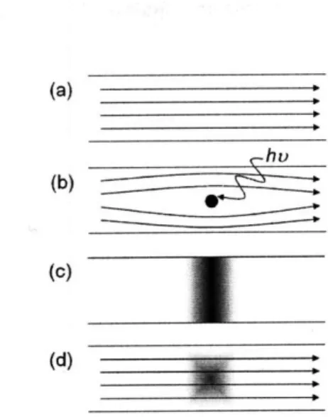
1-1 Schematics of a superconductive nanowire single-photon detector. . . 16 1-2 The hot-spot model for superconductive nanowire single-photon
detec-tors: (a) The 100 nm wide, 4 nm thick nanowire is biased close to its critical current. (b) Once a photon is absorbed by the nanowire, a re-sistive region called hot-spot is formed, and the current is squeezed into the sidewall around the hot-spot. (c) The cross section of the nanowire become resistive. Most of the current goes through low impedance channel, the transmission line (not shown), instead of the nanowire. (d) The energy dissipates, and the resistive region disappears... . 17 2-1 The fundamental Gaussian beam and its characteristic parameters. w:
spot-size; MFD: mode-field diameter; Obeam: spreading angle . . . . . 22 2-2 The relative position of the detector with a radius rd and the beam.
The detector is centered at the origin and the beam is centered at
(xg, yg, zg), while zg is not shown. The distance between the center of
the detector and the center of the beam in the XY plane is r0. The dashed line indicates the spot-size of the beam in the XY plane. Tilt is not considered . ... 25 2-3 The relative tilt between the detector and the beam. d and g are
the norm of the detector surface and the propagation direction of the beam, respectively. They are not necessarily parallel. (a) An XY view; (b) an XZ view . . . .. . . . .. . . . . 26 2-4 The model to treat the tilt as a tilting factor T(d, g) . . . . 27
2-5 The calculated dependence of the coupling efficiency on the radius of the detector. The radius of the detector fabricated is 1.5 - 5 jm, as
shown by two thin dashed lines . ... .. 29
2-6 The calculated dependence of the coupling efficiency on the longitudi-nal misalignment . ... . 29
2-7 The calculated dependence of the coupling efficiency on the lateral misalignment . ... . 30
2-8 The calculated dependence of the coupling efficiency on the angular misalignment . ... .. 31
2-9 The calculated tilting factors . ... .. 31
3-1 Top-down scanning electron micrograph of an 8 tm square supercon-ductive nanowire single-photon detector before dry etching. The image was taken using a Zeiss/Leo Gemini 982 scanning electron microscope with a magnification of 8000. The gun voltage was 5 kV, and the filament current was 199.8 jA . ... . 37
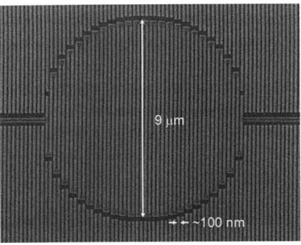
3-2 Top-down scanning electron micrograph of a 9 jm-in-diameter round superconductive nanowire single-photon detector before dry etching. The image was taken using a Zeiss/Leo Gemini 982 scanning electron microscope with a magnification of 8000. The gun voltage was 5 kV, and the filament current was 199.8 gA ... . . . . . . . . ..... 38
3-3 The probe station used for screening detectors . . . ..... .. 38
3-4 The room temperature resistance of the devices . . . ..... . 40
3-5 Linear fit (solid line) of the resistance of the nanowires with different lengths. The slope is proportional to the sheet resistance of the film as-suming the width of the nanowire is uniform. The error bars represent the standard deviations of the measurement .. . . . . . . . .... 40
3-6 The critical current of the devices. . ... 41
3-7 The IcA product of the devices . ... .. 41
4-1 A photograph of the dewar for immersion testing of the superconduc-tive nanowire photon-counters . ... ... .. 44 4-2 The working principle of the nanopositioner. A periodical voltage pulse
(b) is applied to the piezo (a), and due to the inertia, the mass M keeps moving along x-direction (c) . ... .. 45 4-3 The output beam from the fiber focuser measured by the beam scanner.
(a) A 2D graph: different lines indicates different intensities. The mode field diameter is about 6 pm. (b) A 3D graph. The beam is Gaussian-like. 48 4-4 The mode field diameters at different positions of the output of the
fiber focuser. (a) X-axis; (b) Y-axis. The error bars represent the standard deviations of the measurement. .... . . . . . . . . ..... 48 4-5 The mode field diameters at different positions of the output of a
single-mode fiber . (a) X-axis; (b) Y-axis. The error bars represent the standard deviations of the measurement . ... ... .. 48 4-6 The probe for immersion testing with back-illumination . . . . 49 4-7 Bias and readout circuit, and the optical illumination . . . . 50 4-8 Resistance vs. temperature. Above critical temperature, the resistance
of NbN film increases while the temperature is dropping. The critical temperature is about 10.7 K and the residue resistance is about 150 Q. 51 4-9 Output voltage pulses of the detector . ... ... 51 4-10 A single output voltage pulse . ... . 52 4-11 System-detection-efficiency (solid square) and dark-count rate (circle)
of the detector at different bias current. ... . . . . . . . . ..... 52 4-12 The count rate increase linearly with the input optical power... . 53 5-1 A photograph of the cryocooler used for this project . . . . 56 5-2 A schematics of Gifford-MaMahon cryocooler, reproduced from [2]. . 57 5-3 Gifford-MaMahon cycle, reproduced from [2] . . . ..... . 57
5-4 System-detection-efficiency and the dark-count rate as a function of bias current. The error bars represent the standard deviations of the m easurement . ... .... ... 59 5-5 A log-log plot of counting rate vs. optical input power at large bias
current 20 RA. The solid squares are measured data, and the sold line is the linear fitting. ... 60 5-6 A log-log plot of counting rate vs. optical input power at low bias
current 13.4 RA. The solid squares are measured data, and the sold lines are the linear fittings ... 61 5-7 The mechanical part designed for integrating the chip, the fiber focuser
List of Tables
3.1 Categories of devices with different I, and R . . . ..... .. 39
Chapter 1
Introduction
1.1
Background
In many photonic systems for quantum information processing, efficient photon coun-ters are extremely important because any dissipation or loss in such systems will even-tually make the systems degenerate and revert to classical behavior, and many inter-esting quantum properties of photons would therefore become unavailable. Quantum entanglement[3] is one of the most intriguing phenomena in quantum mechanics, and fundamentally, it is the basis for almost all the applications in quantum information science and technology. A good example of such an application is quantum key distri-bution(QKD) based on entangled photons, which has already been demonstrated in metropolitan area networks[4, 5]. However, extending QKD to "long-haul" distances requires simultaneous availability of both bright sources and high-efficiency detec-tors; optical loss in the quantum channel will eventually cause the degeneration of the entanglement and will limit the distance of the QKD. Therefore, a long-distance, large-capacity quantum key distribution system still does not exist because of the lack of the above-mentioned bright entangled photon source and high efficiency receiver.
For any fiber-based, long-haul optical communication system, the major optical loss is caused by the absorption of the fiber. Therefore, to minimize this loss, the wavelength of the light must meet the lowest absorption window of the fiber, which is at 1550 nm. However, an efficient infrared photon counter is difficult to achieve,
Figure 1-1: Schematics of a superconductive nanowire single-photon detector.
compared with its visible counterparts because the energy of a single infrared photon is much smaller than that of a visible one. Some existing technologies, such as semi-conductor PIN photon counters, suffer from low efficiency and high dark-count rates.
Superconductive nanowire single-photon detectors (SNSPD) are an emerging, ultra-sensitive photon-counting technology that is especially useful at infrared wavelengths. SNSPDs are usually made of thin niobium nitride (NbN) film (about 4 nm thick) on top of sapphire substrate, and the NbN film is fabricated into a structure of nanowire (about 100 nm wide) meander, as schematically shown in Figure 1-1. Its working principle is described by the so-called hot-spot model[6}, as shown in Figure 1-2. The nanowire is biased close to its critical current [Figure 1-2 (a)], and once a photon is absorbed by the nanowire, the photon will generate thousands of quasi-particles. These quasi-particles will then diffuse and form a resistive region, a hot-spot [Fig-ure 1-2 (b)]. Therefore, the current will be squeezed into the sidewall around the hot-spot, and the equivalent current density will increase. If this current density ex-ceeds the critical current density of the nanowire, the whole cross section will become resistive [Figure 1-2 (c)}. Thus, a detectable voltage signal will be generated. It is this multiplication process intrinsic to the superconductive nanowire, in which one photon generates thousands of quasi-particles, that makes SNSPD very efficient. Its
(a)
(b)
(c)
(d)
Figure 1-2: The hot-spot model for superconductive nanowire single-photon detectors: (a) The 100 nm wide, 4 nm thick nanowire is biased close to its critical current. (b) Once a photon is absorbed by the nanowire, a resistive region called hot-spot is formed, and the current is squeezed into the sidewall around the hot-spot. (c) The cross section of the nanowire become resistive. Most of the current goes through low impedance channel, the transmission line (not shown), instead of the nanowire. (d) The energy dissipates, and the resistive region disappears.
low-temperature operation (usually 4 K or 2 K) makes the dark-count rate negligibly small so that the detector can conveniently work in a free-running mode. Due to these advantages, an SNSPD was successfully used in a single-photon-based QKD demo-system recently[7].
1.2
System-detection-efficiency of a
superconduc-tive nanowire single-photon detector
The system-detection-efficiency of an SNSPD, q, can be expressed as[1]
R= 1k X 17A X Pr, (1.1)
where qc is the coupling efficiency, determined by the spatial overlap between the optical mode and the active area of the detector; 7A is the absorptance of the NbN
film, determined by factors such as the thinkness of the NbN film, the incident angle (d)
-of the photon and whether there is a microcavity integrated; Pr is the probability -of generating a detectable voltage pulse by one absorbed photon, in other words, not every absorbed photon necessarily generates a voltage pulse. 7A X Pr is referred to as device-detection-efficiency. Because the system-detection-efficiency of an SNSPD is the product of 7c, 7A and Pr, these three factors are equally important, and
there-fore, to enhance the system-detection-efficiency, q, of an SNSPD, one must carefully optimize c, 77A, and Pr.
1.3
The challenges of coupling light to the detector
Our group has successfully developed a robust process to fabricate SNSPDs and has demonstrated device-detection-efficiency above 50% at near infrared wavelengths[8, 1, 9]. One remaining challenge, however, is how to efficiently couple light to the SNSPD. It is challenging because of two reasons. First, the detector works at a cryogenic temperature of 4 K; therefore, the coupling is not as straightforward as that at room temperature. Most optical components are either immersed in liquid helium or stay in a cryocooler, and one needs to control and adjust these optical components from outside. Second, the active area of the detector is small. The detection mechanism determines that the width of the nanowire has to be on a 100 nm scale; therefore, to cover a large area, it requires a very long nanowire, which is difficult to fabricate. So far, the most efficient SNSPD has a 3 tm by 3 jm active area, which is much smaller than the mode field of a single-mode fiber, which is about 10 tm in diameter.
Several steps should be taken to approach high coupling efficiency. First of all, one needs to enlarge the area of the SNSPD without losing detection efficiency, and shrink the spot-size of the light from fiber. Second, one needs a cryogenic setup to characterize the performance of the detectors. Finally, to make the detector truly accessible by other users for various applications, one needs to package the detector so that the light is well coupled to the detector once the fiber is connected.
1.4
Summary of the work in this thesis
This thesis focuses on testing and packaging of SNSPDs, with an emphasize on how to couple light to the detectors.
The thesis begins with a theoretical discussion of the coupling of a single-mode Gaussian beam to a detector, proposes a analytical model, calculates the possible coupling efficiency for certain detector and beam configuration using the model, and obtains the suitable sizes of the detector as well as the sensitivity of the coupling efficiency to the misalignments. These theoretical discussions are the major content of Chapter 2.
In Chapter 3, fabrication of SNSPDs suitable for coupling with a single-mode fiber is described. The screening process used to select devices with good performance is also concisely described.
In Chapter 4, helium-immersion testing of SNSPDs inside a dewar using a probe designed by the author is described. In such a probe are integrated a chip-holder, a fiber-focuser, three nanopositioners, a temperature sensor, and electrical connections. The fiber-focuser is used to shrink the spot-size of the light from a single-mode fiber down to 5 Ipmn, and the nanopositioners are used to accurately adjust the position of the spot in situ three-dimensionally. The detector is directly connected with an SMA connector through wire bonding. The detector is characterized by measuring its resistance as a function of temperature, system-detection-efficiency, dark-count rate, and the counting-rate vs. optical input power.
In Chapter 5, a more convenient, plug-in SNSPD system based on a closed-cycle, two-stage cryocooler is discussed. The major advantage of the cryocooler over the dewar is that it does not need filling with liquid helium. Therefore, this SNSPD system can facilitate many experiments in the field of quantum optics.
Chapter 6 summarizes and concludes the thesis, and possible directions of future work are briefly outlined.
Chapter 2
A theoretical model for coupling
efficiency
To couple light to a detector, one needs to maximize the overlap of the spatial mode of the light with the active area of the detector. Misalignments can decrease this overlap, and therefore, decrease the coupling efficiency. There are three types of misalignments: longitudinal, lateral, and angular. In this chapter, these three mis-alignments and how they affect the coupling efficiency are discussed in detail. A model for coupling efficiency is proposed, which guides the design of the testing setup for superconductive photon counters.
2.1
Gaussian beam and its propagation
One of the simplest beam solutions of Maxwell equations in a homogenous medium is[10]
wo kT2
E(x,y,z) = Eo exp{-i[kz - (z)]- i - }, (2.1)
w(z) 2q(z)
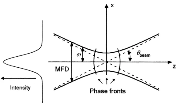
which is referred to as the fundamental Gaussian beam solution. The intensity profile of a propagating Gaussian beam towards z-direction is shown in Figure 2-1. In Eq. 2.1, E is the electrical field, w0 is the spot-size at the beam waist, w(z) is the spot-size at the position z, k is the wave vector, q(z) is the phase parameter, and q(z) is the q
Z
Figure 2-1: The fundamental Gaussian beam and its characteristic parameters. w: spot-size; MFD: mode-field diameter; Obeam: spreading angle.
parameter. Some useful and important relations among these parameters are listed below to facilitate further discussions:
21rn
k
=
,
(2.2)
where A is the wavelength and n is the refractive index of the medium.
z2
w
2(z)
=
o(1 +
-),
(2.3)
zo
where zo = " A . We define mode-field diameter (MFD) as 2w(z), which is also a
commonly used parameter for Gaussian beam, as shown in Figure 2-1.
Obeam tan-1 ( A ) •• (2.4)
7"won 7"won
where the approximation is valid if 9beam <7r/2.
1 1 A
q(z) - R(z) 7rnw2(z)' (2.5)
22
A
where R(z) is the radius of the phase front at z. Eq. 2.5 is the definition of the q parameter.
Several remarks are necessary: (1) For a given wavelength A and a medium (n), the only free parameter for a fundamental Gaussian beam is wo, i.e., the spot-size at its beam waist. Once wo is given, the shape of the fundamental Gaussian beam is fully characterized. (2) The spreading angle Obeam is inversely proportional to wo as shown in Eq. 2.4. This relation is fundamentally due to Heisenberg's uncertainty relation, indicating that a fundamental Gaussian beam with a smaller spot-size at its beam waist will diverge faster. (3) Finally, q(z), summarizing the information of both intensity and phase, is an important parameter that is routinely used to describe the propagation of the Gaussian beam.
The propagation of the fundamental Gaussian beam in a lens-like medium is described by the ABCD law:
Aq + B (2.6)
q2 = Cq .+D (2.6)
Cq2 + D'
The lens-like medium includes optical components such as free-space, thin lenses, dielectric interface, and spherical mirror. Each medium has an ABCD matrix M
A B
M =
(2.7)
C D
associated with it. Eq. 2.6 shows the input-output relation of a fundamental Gaussian beam traveling through a lens-like medium. When a beam propagates through several lens-like media, their matrices can be multiplied together as if the beam were traveling through an equivalent medium with an equivalent matrix:
M = MnMn-1...M1. (2.8)
The simple ABCD law is powerful in describing the propagation of a fundamental Gaussian beam in lens-like media except for one limitation: only a few media are lens-like; therefore, most media cannot be described by a 2 x 2 matrix. For example, if a thin lens is not aligned well so that its norm is not parallel to the
propagation-direction of the beam, ABCD law cannot be applied to such a tilted system. Instead, a generalized matrix can be used[11. However, for most media, neither an ABCD matrix or a generalized matrix can be used.
2.2
Coupling efficiency
In this section, a model for coupling efficiency is proposed, and the effect of three types of misalignments on the coupling efficiency are discussed.
2.2.1
A model for coupling efficiency
Coupling efficiency is determined by the spatial overlap between the optical beam and the active area of the detector. One needs to maximize this overlap in order to minimize the optical loss due to the coupling. Theoretically, complete coupling can be achieved only if the active area of the detector is infinitely large because the Gaussian beam extends to infinity in the XY plane. However, simple calculation shows that 86.5% of the energy is within the spot r < w(z) for the fundamental Gaussian beam. Because of this, the spot-size w(z) is an appropriate spatial scale to which the dimension of the detector should be compared.
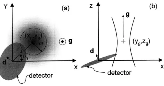
I propose here a simple, but general, model to investigate the coupling efficiency. Consider an SNSPD that has a round-shaped active area with a radius rd. Its center is located at (Xd, Yd, Zd); the normal vector of its surface is d. For the fundamental Gaus-sian beam, the center of the beam waist is at (xg, yg, zg) and its propagation-direction is g. Its spot-size at the beam waist is wo. There are three types of misalignments: (1) longitudinal misalignment: zg / Zd, i.e., the detector is not at the beam waist; (2) transverse misalignment: (xg, yg) 5 (Xd, Yd), i.e., the detector and the beam are not concentric; (3) angular misalignment: d - g
$
1, i.e., there is a certain relative tilt between the detector and the beam. That is why one needs to perform a five-dimension adjustment (x, y, z, and two angular five-dimensions) to achieve good optical alignment.Yt
X
Figure 2-2: The relative position of the detector with a radius rd and the beam. The detector is centered at the origin and the beam is centered at (xg, yg, zg), while zg is not shown. The distance between the center of the detector and the center of the beam in the XY plane is r0. The dashed line indicates the spot-size of the beam in
the XY plane. Tilt is not considered.
and lateral misalignment first. We center the detector at the origin of the coordinate system, i.e., (Xd, Yd, Zd) = (0, 0, 0), and center the beam at (Xg,yg, zg), as shown in
Figure 2-2.
The overlap integral is therefore:
Overlap =
JA
exp{-2[(x - xg)2 + (y - yg)2]/[w(z = 0)]2}dS (2.9)where A is the active area of the detector, w(z = 0) = wo 01 + (0 - zg)2/z2, dS is
the area-element, and the factor 2 inside the bracket of the exponential is due to the intensity integral. To obtain the coupling efficiency, this overlap integral should be normalized by the total flux of the Gaussian beam:
Flux =
J
exp{-2[(x - xg)2 + (y - yg)2]/[w(z = 0)]2}dS (2.10) We treat the tilt as a tilting factor T(d, g). Physically, tilt makes the effectiveY
(a)
X
-U L•..oiLUI
Figure 2-3: The relative tilt between the detector and the beam. d and g are the norm of the detector surface and the propagation direction of the beam, respectively. They are not necessarily parallel. (a) An XY view; (b) an XZ view.
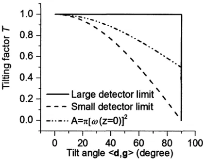
area of the detector smaller because the effective active area is projected onto the XY plane, as shown in Figure 2-3. Avoiding making the integral complicated, an approximation is proposed here to treat the tilt by multiplying the coupling efficiency by this tilting factor. Let us discuss two extreme cases for T as below:
Case 1: A/[w(z)J -- c0, Tz = 1 if d -g = 1; T, = 0, otherwise.
Case 2: A/[w(z)] - 0, T2 = d -g = cos(< d, g >), where < d,g > is the angle
between d and g.
The tilting factors for these two cases are accurate; for all other cases, i.e., 0 <
A/[w(z = 0)] < c0, T satisfies T2 < T < T1. In reality, the active area of our detector is comparable to the spot-size at the beam waist. In this case, we approximate T(d, g) by:
AT1 + ir[w(z = 0)2 (2.11)
T(dg) A + A r[w(z = 0)]2
that is, T1 and T2 are weighted by the area A of the detector and the characteristic area of beam r[w(z = 0)12, respectively. Using Eq. 2.11 for the case that A = w[w(z = 0)]2,
1.0-
0.8-04
0.6-
S0.4-
0.2-
0.0-I I j I I I I I p I I0
20
40
60
80
100
Tilt angle <d,g> (degree)
Figure 2-4: The model to treat the tilt as a tilting factor T(d, g)
angle because Tl-line and T2-line are close to each other. Thus, applying the above discussion to our round-shape detector, an analytical expression for the coupling efficiency is obtained:
Tf
fAexp{-2[(x - xg)2 + (y - yg)21/[w(z)]2}dS(rdT)
f
f%
exp{-2[(
xg) 2+
(y - yg)2]/[W(Z = 0)]2}dS(2.12) where the dependence on the area of the detector (rd), the shape of the beam (w0), the longitudinal misalignment (zg), the lateral misalignment(xg and yg), and the tilt
(T) are explicitly shown. Therefore, Eq. 2.12 summarizes all the discussions in this
section.
2.2.2 Numerical results
A numerical integral was used to examine the dependence of 7ic on other parameters. In reality, two types of Gaussian beams are important: the first is the output beam of a single-mode fiber with w0 = 5 in, the beam waist of which is exactly at the facet of the fiber; the second one is the output beam from a fiber focuser with wo = 2.5 Wm, the
%% %%
-
Large detector limit
- - -
Small detector limit
"beam waist of which is several millimeters away from the output lens (this distance is called working distance). Therefore, we set wo = 5 ýtm and 2.5 ýtm in our discussion and focus on these two cases. Now let us discuss the effect of the size of the detector, as well as the longitudinal, transversal and angular misalignments, respectively.
Size of the detector
Assume w(z = 0) = wo, ro = 0, and T = 1, i.e., there is no misalignment, and the only
parameter that determines the coupling efficiency is the radius of the detector. As shown in Figure 2-5, the coupling efficiency monotonically increases with the increase of the size of the detector, sharply at the beginning, then reaches a plateau and slowly approaches the upper bond of one. In addition, the dashed line for the fiber focuser is above the full line for the fiber, meaning that for the same detector, the coupling efficiency for the small spot is higher, which matches the intuitive analysis. Furthermore, the radius of the detector fabricated is 1.5-5 ýLm (shown as thin dashed lines in Figure 2-5); to make the coupling efficiency reach the plateau, a fiber focuser is necessary and the radius of the detector should be 3.5 - 5 ýtm.
Longitudinal misalignment
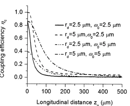
Now let us focus on the longitudinal misalignment zg. As representative examples, four combinations of (rd and wo) are calculated and shown in Figure 2-6. One can see that the coupling efficiency decreases quickly with the longitudinal misalignment. For example, consider this scenario: if we perform back illumination using a bare fiber, due to the 500 tm thickness of the sapphire substrate, the minimum longitudinal misalignment is therefore 500 jtm. For simplicity, we do not take into account the refractive index of the sapphire. In this case, the coupling efficiencies are all below 10% for all four cases. Considering the requirement of back-illumination, we see that a fiber focuser is important. On the other hand, the beam from the fiber focuser diverges faster, and therefore has more stringent requirements on the longitudinal alignment. One can see that the beam with a waist of wo = 2.5 jm decreases more quickly in coupling efficiency than its wo = 5 jim counterpart.
1.0
> 0.8 o 0 • 0.6 0) 0.4 0 0.2 0 0.0 0 1 2 3 4 5 6 7 8Radius of the detector (trm)
Figure 2-5: The calculated dependence of the coupling efficiency on the radius of the detector. The radius of the detector fabricated is 1.5 - 5 rtm, as shown by two thin dashed lines. 1.0
-
0.8-)0.6-) 0.4-C 0
O
0.0
o
0.0-\
S
-rd=2.5
~tm,w=2.5 Pm
.
--
rd=5
ýim,%=2.5
pm
-...
rd=2.5 pm,
Jom=5
m
S\ ---rd=jm,
(,,=5jtm
' I I I I I0
100
200
300
400
500
Longitudinal distance z ('m)Figure 2-6: The calculated dependence of the coupling efficiency on the longitudinal misalignment.
1.0-> 0.8-0 .$
S0.4-
0.6-•-
0.2-
0.0-rd= 2 .5 pm, co0=2. prm N2. S,, - - rd= 5 1m,(o=2.5 ptm re=2.5 pLm, c,=5 -tm , *r- rd= 25 . pm, )o=5 pm \\ = - N. -. =\0
2
4
6
8
10
Lateral misalignment r
o(pm)
Figure 2-7: The calculated dependence of the coupling efficiency on the lateral mis-alignment.
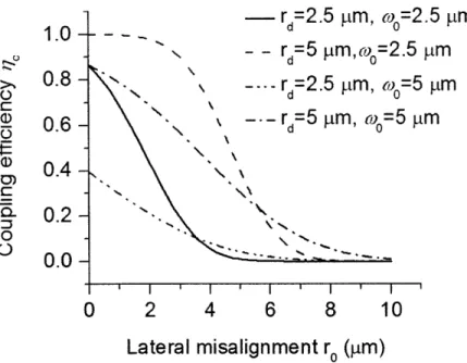
Lateral misalignment
Suppose we now have only lateral misalignment. As shown in Figure 2-7, the result of 10 ýtm lateral misalignment is that almost no light is coupled. In addition, a large
detector and a small beam (rd = 5 jtm, w0 = 2.5 jim) are favorable because this
con-figuration not only achieves high coupling efficiency but also allows more lateral mis-alignment tolerance. From this figure, we learn that if we use positioners/translation stages to adjust the beam, the step size has to be smaller than 1 jtm.
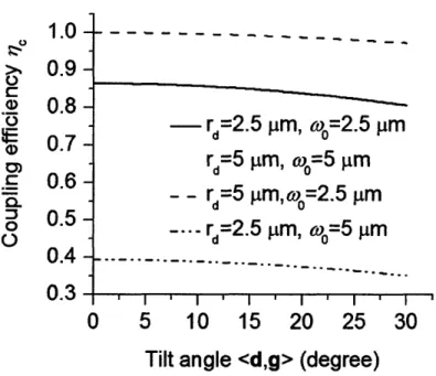
Angular misalignment (tilt)
Figure 2-8 shows the dependence of the coupling efficiency on tilt within a tilt-angle range from 0 to 30 degrees. Larger tilting angles can be avoided by a careful mechan-ical design; therefore, they are not important in our calculation. One can see that the tilt only affects the coupling efficiency slowly, meaning that the tilt has relatively large tolerance compared with longitudinal and lateral misalignment. The tilting factors are separately shown in Figure 2-9.
1.0 0.9
0.8- 0.7- 0.6-
0.5-
0.4-0.3rd=
2.5 pm,
%=2.5
pm
rd=5pm, %=5
pm
- - rd=5
prm,%=2.5 pjm
. rd=
2.5
pm,w=5 prm
0
5
10
15
20
25
30
Tilt angle <d,g> (degree)
Figure 2-8: The calculated dependence of the coupling efficiency on the angular misalignment.
1.00-
0.98-
0.96-
0.94-
0.92-0.90
0.88
rd=2.5 m,
c%=2.5
pjin..
rd=5 pm, %=5pJm
- - rd=5gm,%=2.5
p
mrd=
2.5 im, %=5
pm
I I I I II0
5
10
15 20
25
S3030Tilt angle <d,g> (degree)
Figure 2-9: The calculated tilting factors.
>, :oU 0 0') ._ 0 0 . I ' I ' I ' I ' I ' IT
-2.2.3
Remarks on the model
Several remarks are necessary:(1) We have discussed the dependence of the coupling efficiency on the detector size, the longitudinal, lateral, and angular misalignments, respectively. In reality, however, these factors coexist and not separable, and therefore, one needs to use Eq. 2.12 to calculate the coupling efficiency if necessary. However, the significance of this model does not rest on predicting the efficiency exactly because the misalignments are difficult to measure in our experiment. The significance of the model is to predict the trends, calculate the bounds of the coupling efficiency for different configurations, determine the important parameters, and therefore guide the design of the experiment
setup.
(2) The calculation above shows that for the experiment, a fiber focuser is neces-sary, the detector size should be rd C [3.5 [im, 5 im], the tilt is not as important as the lateral and longitudinal alignment, and the step size for the positioners for lateral misalignment correction should be on the order of hundreds of nanometers. These conclusions serve as the guides for the design of the experiment setup.
(3) The model proposed and discussed above can be trivially modified so that it can be applied to a square detector. Because a square detector is less symmetrical compared with a round detector, some discussions will become slightly more compli-cated; for example, the coupling efficiency will obviously become direction-dependent on the lateral misalignment. However, the trends discussed above for round detectors apply to the square detectors.
(4) We have discussed alignment between the beam and the detector, but have not elaborated how the beam propagates, for instance, through the sapphire substrate, although the ABCD law is briefly outlined. To discuss the propagation, one can implement the ABCD law.
(5) The beam at the detector surface may not necessarily be a perfect fundamental Gaussian beam, considering the scattering of the dust or defects on the lens and on the detector. Essentially, we only consider the effect of the spatial overlap here. The
scattering loss by the dust or defects on the lenses is included in the loss of the fiber, and the scattering loss by the dust or defects on the detectors is included in the absorption of the detector. Both of them are out of the scope of the discussion in this chapter.
(6) Finally, it is noteworthy that not only the coupling efficiency, ?c, but also the absorptance of the NbN film, rA, depend on the tilt. The effect of the tilt on the absorption of the NbN film is out of the scope of the discussion here.
2.3
Summary
In this chapter, the coupling efficiency has been discussed theoretically and a general, analytical model is proposed. This model can be applied to any light-to-detector coupling problem. The major advantage of this model is that the treatment of the tilt is greatly simplified.
Based on the calculation of the dependence of the coupling efficiency on the detector-size, longitudinal, lateral, and angular misalignments, it is recommended that (1) a fiber focuser is necessary; (2) the detector size should be rd E [3.5 .m, 5 mi); (3) the tilt is not as important as the lateral and longitudinal alignment; (4) the step size for the positioners for lateral misalignment correction should be on the order of hundreds of nanometers or smaller.
Chapter 3
Fabrication and screening of the
detectors
Our group has developed a robust process for fabricating NbN superconductive nanowire single-photon detectors[8, 1]. This process includes three major parts in sequence:
(1) fabrication of gold pads; (2) fabrication of nanowires; and (3) addition of cavities as well as anti-reflection coating (ARC). Each part is composed of several steps.
Although the process is simple and straightforward, the yield is not 100% due to the imperfection of the film and of the process. In particular, the yield decreases with increasing size of the detector, and therefore there is a compromise between achiev-ing a large-area detector for couplachiev-ing and the probability of obtainachiev-ing such a large area detector with high device-detection-efficiency. Because the yield is not 100%, a screening process is necessary to select good devices before testing and packaging. The major apparatus for this screening process is a probe station.
3.1
Fabrication of the detectors
A round detector has the largest possible overlap with a Gaussian beam compared with other types of detectors that have the same length of nanowire. Furthermore, it is concluded in Chapter 2 that the radius of the detector should be between 3.5 jtm and 5 ltm. As we do not know exactly how fast the yield decreases with the increase
of the length of the nanowire, we fabricated several different types of detectors for this project, including (1) square detectors with dimensions of 3 xmx3 jim, 6 jmx6 pm, 7 m x 7 pm, 8 jmmx8 jm, and 9 m mx9 pmrn; (2) round detectors with diameters of 6 jm, 7 Rm, 8 in, and 9 gm as well as (3) 5 im x 10 im detector pairs.
The first part of the process was making gold pads. A wafer from Moscow State Pedagogical University or from Lincoln Laboratory was cut into 8 x 8 gm2 square. The
chips were cleaned using acetone so that no more than 1 or 2 particles are inspected under the microscope. Pattern exposure was done by contact optical lithography (Tamarack) with an intensity of 3.3 mW/cm2 and 15 second exposing time, and the
resist used here is S1813, spun at 6 krpm to make a one micrometer thick layer. To create an undercut structure to facilitate the liftoff process, one important step before developing the pattern using Microposit 3552 NaOH developer (3 minutes) was dipping the chip in chlorobenzene for 15 minutes. After development, 10 nm Ti and 50 nm Au were evaporated followed by a liftoff process in hot N-methyl pyrolidinone
at 90 VC.
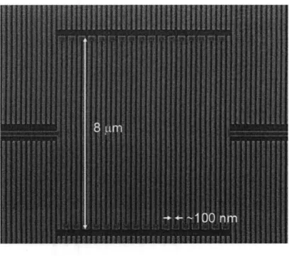
The second part of the process was making meanders. The pattern was defined by scanning electron-beam lithography (Raith) using a negative tone resist hydrogen-silsesquioxane (HSQ). Before spinning HSQ, the chip was immersed in 25% Tetram-ethylammonium hydroxide(TMAH) for 4 minutes to remove contamination leftover from photoresist, which helped avoid adhesion problems of HSQ on NbN. The thick-ness of HSQ on the chip was targeted at 100 nm. The meander was exposed on Raith at 30 KeV using an appropriate dose selected by running a dose matrix. The proximity-effect was corrected by adding redundant nanowires around the meander of the detector[121. After 4-minute development inside 25% TMAH, RIE (Plasmath-erm) CF4 dry etching with voltage of 20 V and power of 100 W was performed for 90 seconds, followed by the inspection using scanning electron microscope(SEM). Figure 3-1 and Figure 3-2 show SEM images of an 8 jm square and a 9 jm-in-diameter round detectors, respectively, before dry etching.
The last part of the process was adding a cavity on the top and ARC on the back of the substrate. The major steps were: (1) spinning HSQ with an appropriate thickness
Figure 3-1: Top-down scanning electron micrograph of an 8 pum square superconduc-tive nanowire single-photon detector before dry etching. The image was taken using a Zeiss/Leo Gemini 982 scanning electron microscope with a magnification of 8000. The gun voltage was 5 kV, and the filament current was 199.8 tiA.
on top of the device; (2) e-beam exposure to define the cavity; (3) evaporation of Ti/Au layer; (4) a metal liftoff process to deposit the mirror; (5) ARC coating on the back. For details of the processing, one can refer to reference [1]. It is noteworthy that the thickness of the HSQ should be carefully controlled because this cavity length determines the central wavelength of the absorption.
3.2
Screening the detectors
There were more than 200 devices on one chip, among which some best candidates were selected for further testing and packaging. This step was screening, performed in a probe station as shown in Figure 3-3. The chip was mounted on a chip-holder using some silver-paint, the function of which was not only to attach the chip onto the chip-holder, but also ensured a good thermal contact between them. The chip-holder was mounted in the probe station.
IcR product is the criteria for selecting good devices, where Ic is the critical current
8 UM
Figure 3-2: Top-down scanning electron micrograph of a 9 Lm-in-diameter round superconductive nanowire single-photon detector before dry etching. The image was taken using a Zeiss/Leo Gemini 982 scanning electron microscope with a magnification of 8000. The gun voltage was 5 kV, and the filament current was 199.8 IpA.
Table 3.1: Categories of devices with different Ic,, and R. Device category Ic R Cross section
A large large Appropriate, uniform, and nonrestricted B small large Too small or restricted
C large small Too large, or many footings
D small small Too large or many footings, and restricted
and R is the room temperature resistance. IcR product gives the information of the quality of the nanowire fabricated, as shown in table 3.1. A nanowire with a large IcR product is with an appropriate width, uniform, and nonrestricted; the corresponding detector usually has a good device efficiency. To compare different types of devices with different lengths but the same width of the nanowires in this project, IcA product should be used, where A is the resistance per unit length of a nanowire.
The room temperature resistance is shown in Figure 3-4. Note that if the nanowire is broken, its resistance is infinite; but on Figure 3-4, the resistance is set to be zero for this case to make the figure more readable. On this chip, several types of devices were fabricated, and one can see the linear increase of the resistance of the nanowire with its length, based on which the sheet resistance can be obtained by a linear fitting of the resistance-length data, as shown in Figure 3-5. The sheet resistance at room temperature is about 371 Q/0.
After cooling the devices in the probe station down to 4.1 K, the critical current of each device was measured, as shown in Figure 3-6. The critical current was measured by slowly increasing the bias current, and once the current suddenly drops, the current before dropping was the critical current. The measurement was repeated on each device three times to eliminate the errors due to the noise and the fluctuation. From Figure 3-6 one can see that the critical currents for most devices are around 15
pA. Occasionally, the critical current is too large or too small, indicating that the corresponding devices are useless.
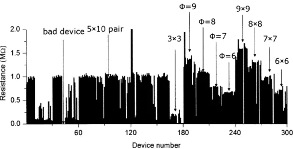
IcA product is shown in Figure 3-7. The devices with large IcA products presum-ably had no processing defects and had good local film quality. The statistics of the IcA products for the whole chip with 300 devices in total is shown in Figure 3-8. One
2.0- bad device 5x10 pair 1.5 1.0- 0.5- 0.0-60 120
0=9
0=83x3| 0=7,
1809x9
8x8
7x7
240 300 Device numberFigure 3-4: The room temperature resistance of the devices.
1.6
1.2-0.8
0.4
0.0
----
slope=0.00371
0100
200
300
400
Length of the nanowire (pm)
Figure 3-5: Linear fit (solid line) of the resistance of the nanowires with different lengths. The slope is proportional to the sheet resistance of the film assuming the width of the nanowire is uniform. The error bars represent the standard deviations
of the measurement.
25 20 15 10 5 0
I
I
60 120 180 240 Device number 300Figure 3-6: The critical current of the devices.
0.08 0.06 0.04 0.02 0.00 50 100 150 200 250 Device number 300
Figure 3-7: The IcA product of the devices.
can see that about 8% of the devices have IcA products larger than 0.7 ýtAMQ/ýLm, and the following testing and measurement will focus on these devices. 50% of the devices have medium IcA products between 0.5 and 0.7 ýtAMQ/ptm, and 13% of the devices are "dead" devices with very low IcA products smaller than 0.1 pAMQ/p.m.
3.3
Summary
In this chapter, the fabrication and the screening of the detectors are described. Round-shaped detectors with appropriate sizes have been fabricated for this project.
I
80
70
60
50
40
30
20
10
n
13%
6%
5
25% 25%
E%<
1%
0.00 0.02 0.04 0.06 0.08 0.10 ICA (pA MfYpm)Figure 3-8: The statistics of the IcA product of the devices fabricated.
It has been pointed out that normalized IcA product is the number to characterize the quality of the film and of the process.
L__~
~ -4
k---Chapter 4
Immersion testing of the detector
inside liquid helium
When the superconductive nanowire single-photon counter is working, its temperature much be kept below the critical temperature, which is about 11 K. One way to keep such a low temperature is to immerse the device inside liquid helium, and therefore, the device temperature stays at the boiling temperature of the liquid helium, around 4 K. A widely used apparatus to perform this immersion testing of superconductive devices is a dewar, named after its inventor, a Scottish chemist and physicist, Sir James Dewar (1842-1923). The advantage of the dewar, compared with a cryocooler, is that it is easy to keep a constant temperature as long as the device is immersed. The disadvantage is that it consumes liquid helium fast, and therefore, one needs to continue refilling the dewar as the experiment progresses.
This chapter is devoted to the discussion of immersion-testing of the SNSPD in-side a dewar. In this step, the detector is characterized by measuring its resistance as a function of temperature, system-detection-efficiency, dark-count rate, and the counting-rate vs. optical input power. The design of the experiment setup is elabo-rated, and the experiment results are presented.
Figure 4-1: A photograph of the dewar for immersion testing of the superconductive nanowire photon-counters.
4.1
Experimental setup
The apparatus to perform immersion-testing is composed of two major parts: a dewar and a probe. The dewar was purchased from Janis Research Company and set up by another student Charles Herder in our group. The probe, designed by the author, integrates the chip, the temperature sensor from Lakeshore, the nanopostioners from Attocube, the fiber focuser from Ozoptics, RF connectors and cables. The fabrication of the detectors was introduced in Chapter 3. In this section, the remaining parts are described.
4.1.1
The dewar
The dewar is composed of two chambers: the outer chamber is for liquid nitrogen for thermal insulation, and the inner chamber is for liquid helium. A photo of the dewar for immersion testing is shown in Figure 4-1.
The correct procedure to manipulate the dewar is summarized in the following six steps: (1) fill the inner chamber with liquid nitrogen; (2) fill the outer chamber with
V
AL
(b)
t
Xf
plezzo
Figure 4-2: The working principle of the nanopositioner. A periodical voltage pulse (b) is applied to the piezo (a), and due to the inertia, the mass M keeps moving along x-direction (c).
liquid nitrogen; (3) use nitrogen gas to pump out the liquid nitrogen from the inner chamber; (4) pump the inner chamber so that its pressure drops below certain level; (5) fill the inner chamber with helium gas; and (6) fill the inner chamber with liquid helium. The sequence of these steps must be rigourously followed to avoid possible condensations of either water vapor in the air or of the nitrogen residue. The conden-sations have large heat capacities; therefore, the chamber with these condenconden-sations can only stay around 4 K for a short time.
4.1.2
The nanopositioners
To accurately control the position of the beam waist, we use three nanopositioners to move the fiber focuser in three dimensions. The core of the nanopositioner is a piezo, and the working principle is based on stick-slip inertial motion. When increasing voltage is applied to the piezo, it will extend in one direction. The mass sticks on the piezo, and moves with the piezo in the same direction. When the voltage is shut off suddenly, the piezo will contract back to its original length very quickly, but the mass stands still due to its large inertia, in other words, the mass slips relative to the piezo. This stick-slip process makes the nanopositioner move one step. By repeating this process at a certain frequency
f,
one can continuously move the nanopositioner step by step. The working principle is illustrated schematically in Figure 4-2.Table 4.1: Specifications of the nanopositioners
Temperature t (K) C t (nF)
f'
(Hz)
Step-size (nm) Voltage * (V)300 X=878 single step or 1-80000 50-2000 0-70
4.2 X=146 single step or 1-80000 10-500 0-70
Data source: t measured; ý manufactural data sheet[13J.
The step size of the nanopositioner is dependent on the voltage applied to it and its capacitance C. The capacitance further depends on the temperature, the voltage, and the frequency
f.
The typical values of these parameters are listed in Table 4.1. The traveling range of each nanopositioner is 5 mm.The nanopositioner can be either controlled by a controller unit or by a computer through the control unit. One can easily tune the frequency and the voltage, measure the capacitance of the piezo in each channel, and drive each nanopositioner continu-ously or in a single step manner using the controller. Using the computer to control the nanopositioners, however, one can benefit by two additional functions: one can specify the number of steps, and can program the voltage increasing pattern, that is, linear, exponential, and logarithm.
For our application, the most important parameters are the step-size and the traveling range. The step size should be smaller than the spatial sensitivity discussed in Chapter 2. Fortunately, if we set the voltage low enough, each step with even several 10 nm is possible. The traveling range requires one to make sure that the initial transverse and longitudinal misalignments between the center of the beam and the center of the detector are small enough (< 5mm). Good initial alignments must be ensured by mechanical design.
4.1.3
The fiber focuser
Chapter 2 concluded that the fiber focuser is necessary for the coupling. In this experiment, the fiber focuser is made by Ozoptics: the manufactural specifications
are that the spot-size is 2.5 pnm and the working distance is 3.5 mm. The spot-size of the fiber focuser was measured using a simple experimental setup. The major
apparatus was a beam scanner, which could measure the profile of the beam in situ. Firstly, the beam scanner was aligned with the fiber focuser so that the beam received by the scanner was a Gaussian, as shown in Figure 4-3. The beam scanner could be moved on a track while maintaining the alignment. Secondly, the displacement of the beam scanner was measured by a calibrator and at each position, the spot-size was measured by the beam scanner. Note that the absolute distance between the fiber focuser and the beam scanner is difficult to measure because the sensitive area of the beam scanner is inside a plastic shield. But the relative displacement of the beam scanner can be measured accurately. In this way, one can scan the beam along z-direction, and the spot-size vs. the displacement is shown in Figure 4-4. A linear fitting of the data yields the diverging angle Obeam = tan-lk and the spot-size. However, the directly measured spot-size may not be accurate because the accuracy of the calibrator is not enough for this measurement. Instead, Eq. (2.6) is used to obtain the spot-size:
A
Wo=.
7rtan(½tan-1k)(4.1)
(4.1)Here k is taken to be the average of the 4 slopes (see Figure 4-4) obtained by the fitting, i.e., k = Ei Ikil/4. In this way, the spot-size calculated at the beam waist is 2.85 tm, which is consistent with the data in the manufactural specification.
As shown in Figure 4-5, we use the same method and obtain the spot-size at the beam waist from a single-mode fiber, which is 5.65 tm, or equivalently, the MFD is
11.3 im, which is also consistent with the MFD of the single-mode fiber.
4.1.4
The mechanical design of the probe
The mechanical design of the probe is the part of this project with a simple prin-ciple but a difficult practice. In this project, the major challenge is that the probe needs to integrate several apparatuses together in a small space. Considering back illumination, the probe is designed as shown in Figure 4-6.
Figure 4-3: The output beam from the fiber focuser measured by the beam scanner. (a) A 2D graph: different lines indicates different intensities. The mode field diameter is about 6 gm. (b) A 3D graph. The beam is Gaussian-like.
fiber focuser, x-axis
k=-0.371, b=6.0672 SA'\k=0.346, S b=6.4283 i,,
-1000 -500
0 500
Position (pnm) 400 - 300- 200- 10 0-10 t~' 1000 (b)fiber focuser, y-axis
k=-0.364, ' b=6.54pm k=0.345, l O b=6.615gm q D -1000 -500 0 500 1000 Position (pm)
Figure 4-4: The mode field diameters at different positions of the output of the fiber focuser. (a) X-axis; (b) Y-axis. The error
the measurement. 1000 -800 -600 - 400- 200 -ner
- Linear nI=u. I I O, •oo. UrL
bars represent the standard deviations of
1000- 800- 600- 400- 200-O'
bare fiber, y-axis
ner |,m 0 2000 4000
(a)
Position (pm) (b) 0 2000 Position (pnm)Figure 4-5: The mode field diameters at different positions of the output of a single-mode fiber. (a) X-axis; (b) Y-axis. The error bars represent the standard deviations of the measurement. 400- 300- 200- 100-0 -100 (a)
4000
(a)
6 LIM
-- IvyV I II ~r·~c~iI
u . . ,Chip
-Fiber
focuser
Nano-positioners
Figure 4-6: The probe for immersion testing with back-illumination.
4.2
Experimental results
Several measurements, including resistance vs. temperature, system efficiency and dark count rate vs. bias current, count rate vs. optical input power, were performed to characterize the detector.
The circuit for biasing the detector and the readout, as well as the optical elements, is shown in Figure 4-7. It is composed of a low-noise current source, two bias-Ts to further reduce possible noise from the source, an attenuator to decrease the dark counts, two amplifiers to enhance the output signal, and the oscilloscope to display the pulse or a universal counter to measure the counting rate. After the detector is bonded to an SAM connector as well as ground (not shown in the figure) by gold wires, it is illuminated by a 1550 nm cw laser with an adjustable attenuation. Meanwhile, the light spot is shrunk by a fiber focuser, which has been discussed in detail in section 4.1.2., and the polarization of the incident laser is controlled by a manual polarization controller.
The resistance of the NbN thin film increases as the temperature is decreasing, shown in Figure 4-8. This increase in resistance is probably due to the granular
Bias T1
__ ~ Bias T2 Amplifiers
Current source
Figure 4-7: Bias and readout circuit, and the optical illumination.
property of the NbN film: One mechanism of the transportation of the electron in such a system is "hopping", which is assisted by thermal excitation. Therefore, as the temperature is dropping, this excitation becomes weak so that the film becomes less conductive. When the critical temperature is reached, which is about 10.7 K, the resistance drops abruptly, and there is a small residue resistance of about 150 Q. The origin of this residue resistance is not clear to the author yet, but it should not be larger than 200 Q; otherwise, the detector will become unstable or latched, and all the measurements may not be accurate.
After the laser was turned on and attenuated so that the input optical power was 100 nW, series of pulses were observed on the oscilloscope, as shown in Figure 4-9. A single pulse is shown in Figure 4-10. The pulses were counted using an Angilent universal counter . In this way, the system-detection-efficiency and dark-count rate were measured at different bias currents. The position of the light spot was adjusted by the three nanopositioners. As shown in Figure 4-11, both the system-detection-efficiency and the dark-count rate increased with the bias current exponentially, and approached 10-6 and 104 per second, respectively, when the current got close to the critical current 15.5 IA. The device efficiency of this detector measured at Lincoln