HAL Id: hal-03100915
https://hal.laas.fr/hal-03100915
Submitted on 6 Jan 2021
HAL is a multi-disciplinary open access
archive for the deposit and dissemination of sci-entific research documents, whether they are pub-lished or not. The documents may come from teaching and research institutions in France or
L’archive ouverte pluridisciplinaire HAL, est destinée au dépôt et à la diffusion de documents scientifiques de niveau recherche, publiés ou non, émanant des établissements d’enseignement et de recherche français ou étrangers, des laboratoires
Parseval’s Theorem Used for the Inductor Analysis in
High-Frequency Boost Converters
A. Gutiérrez, Emmanuel Marcault, Corinne Alonso, Jean Paul Laur, David
Trémouilles
To cite this version:
A. Gutiérrez, Emmanuel Marcault, Corinne Alonso, Jean Paul Laur, David Trémouilles. Parseval’s Theorem Used for the Inductor Analysis in High-Frequency Boost Converters. ELECTRIMACS 2019 Selected Papers, pp.347-362, 2020, 978-3-030-56970-9. �10.1007/978-3-030-56970-9_26�. �hal-03100915�
Parseval’s Theorem for the Inductor Analysis in
High-Frequency Power Converters
A. Gutierrez 1∗ , E. Marcault 1, C. Alonso 2, J-P. Laur 2, D. Tremouilles 2
1CEA-Tech Occitanie, Toulouse - France. 2LAAS-CNRS, Toulouse - France
Abstract
Advances in GaN-HEMT devices have encouraged the development of power converters at megahertz-level. However, inductors for high-frequency power converters require innovative approaches to overcome challenging con-straints in both power and frequency. In this context, this paper presents an extension of the Parseval’s theorem for the inductor analysis based on the energy conservation principle in the time and the frequency domains. Our approach aims to provide insights about the inductor power losses using high-frequency parameters and the inductor current harmonics. The pro-posed approach disaggregates the power losses in the frequency-domain for the inductor power signals in the time-domain. Main findings from the pre-sented methodology provide useful selection criteria for inductors in power converters given parameters of quality factor (Q) and Self Resonance Fre-quency (SRF ). Simulation results show the impact of the inductor behavior on the switching losses. An experimental setup validates the proposed ap-proach. A high-frequency boost converter is presented as a study case. Keywords: Power Inductor, Quality Factor, Self Resonance Frequency, Boost Converter, GaN-HEMT.
1. Introduction
Traditional analysis of power converters requires design tools intended to 1
deal with operation frequencies around hundreds of kilohertz [1]. However, 2
outstanding advances in Gallium Nitride - High Electron Mobility Transis-3
tors (GaN-HEMTs) enlarge the operation condition of power converters to 4
the range of megahertz [2][3]. Indeed, this extended bandwidth requires in-5
novative design methodologies to achieve a trade-off between high-frequency 6
and high-power conditions [4]. Additionally, these new generation of power 7
converters should incorporate power inductors with both high current han-8
dling and high operation frequency [5][6]. 9
10
As result, high-frequency parameters become more and more important 11
for the analysis and selection of inductors during the design process of power 12
converters [7][8]. Usually, applications of inductors in high-frequency take 13
into account the manufacturer parameters of Self Resonance Frequency (SRF ) 14
and quality factor (Q). These SRF and Q parameters allow describing the 15
inductor operation bandwidth and the associated power losses. However, 16
these inductor parameters are few analyzed in the conventional design of 17
power converters at kilohertz-level. Conversely, operation at megahertz-level 18
should include the SRF and Q parameters in the design stage. 19
20
Additionally, the switching improvements provided by GaN-HEMTs can 21
extend the operation frequency of power inductors to levels usually dedi-22
cated to radio-frequency applications. However, manufacturing constrains 23
associated to ferromagnetic cores limit the scope of power inductors in high-24
frequency applications [9]. Therefore, manufacturing features and power-25
frequency behavior require a suitable trade-off to improve the inductor per-26
formance in high-frequency power converters [10][11]. 27
28
In this context, we proposed an innovative approach using the Parseval’s 29
theorem as a means to associate the power losses in the time-domain and the 30
inductor behavior in the frequency-domain. The developed framework aims 31
to be complementary to conventional and well known methodologies for the 32
inductor selection and design of power converters. This approach provides 33
insights about the impact of the quality factor (Q) and the Self Resonance 34
Frequency (SRF ) on the inductor current harmonics and the power losses. 35
Simulation results suggest suitable criteria for a trade-off between the quality 36
factor (Q) and the power losses given feasible manufacturing features. Fur-37
thermore, this paper proposes an inductor model incorporating the Q and 38
SRF parameters into a circuital model useful for the analysis of power con-39
verters. 40
41
This paper is organized as follows. Section 2 describes the power and fre-42
quency behavior of power inductors considering high-frequency parameters. 43
Section 3 presents the theoretical approach based on the Parseval’s theorem 44
to study the relation between power and frequency. Section 4 describes the 45
proposed inductor model including SRF and Q parameters. Section 5 ex-46
plains in detail the experimental setup to validate the proposed approach. 47
Finally, an experimental high-frequency boost converter is implemented. 48
2. Power inductor behavior in high-frequency 49
This section describes the inductor behavior in a high-frequency power 50
converter taking into account the quality factor (Q) and the Self Resonance 51
Frequency (SRF ). A high-frequency boost converter is presented as an il-52
lustrative example. 53
54
Fig. 1 shows the designed boost converter as a study case using a com-55
mercial reference of a power inductor. The switching frequency is set to 56
30MHz to take advantage of the switching characteristics of GaN-HEMTs. 57
This boost converter increases the voltage from 200V to 400V with output 58
power of 400W and load of 400Ω. In this design, the inductor is set to 59
8.2µH and the output capacitance is set to 220pF. Furthermore, the studied 60
converter focuses on the inductor performance considering ideal the other 61
components to avoid their influence in the developed analysis. 62
63
Figure 1: High-frequency boost converter with actual inductor and ideal associated com-ponents.
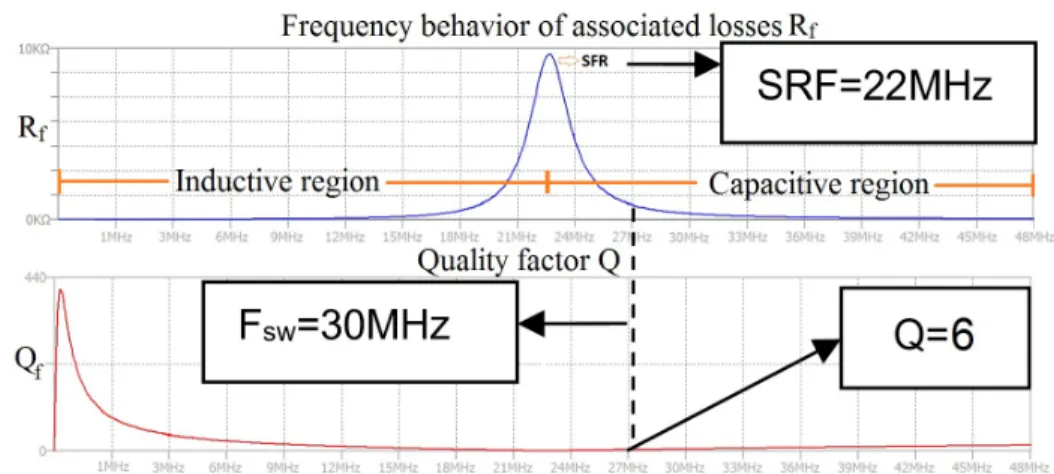
Fig. 2 depicts the frequency behavior of the associated inductor losses 64
Rf and the quality factor Qf for the power inductor of 8.2µH used in the
65
designed boost converter. Additionally, Fig. 2 shows the SRF of the stud-66
ied power inductor. The inductive characteristics prevail in the region of 67
frequencies lower than the SF R and the capacitive characteristics prevail 68
in frequencies higher than the SRF . Rf and Qf of Fig. 2 are calculated
69
using the inductor model provided by the manufacturer. The Rf and Qf
70
parameters depend on the actual inductor impedance Z = |Z| ∠θ. The as-71
sociated losses Rf are defined as the real part of the inductor impedance
72
by Rf = |Z| cosθ. The quality factor Qf expresses the relation between the
73
stored and dissipated energy. The quality factor Qf in an inductor is given
74
by Qf = XL/Rf = tanθL, where XL= |Z| sinθ.
75 76
Figure 2: Frequency behavior of Rf and Qf for the power inductor used in the designed
boost converter.
The power inductor under study accomplish the requirements of induc-77
tance and current in the range of KHz. However, it has a low performance 78
in the range of MHz as shown in Fig. 2. The proposed analysis intentionally 79
begins with this unsuitable inductor to assess and understand the influence 80
of the high-frequency parameters in the inductor performance. This analysis 81
is the first step to define selection criteria for high-frequency power inductors 82
with a suitable trade-off between performance and feasibility. 83
84
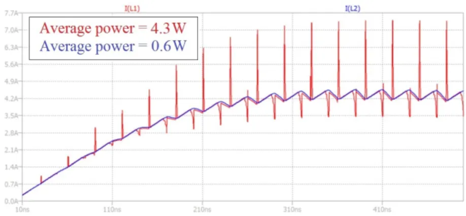
Fig. 3 shows the simulation results comparing the inductor current in the 85
case of an ideal inductor in series with a low resistance and the manufacturer 86
model for the studied inductor. In addition, Fig. 4 illustrates the current har-87
monic spectrum of the inductor under analysis. Results from Fig. 2 to Fig. 88
4 show that the unsuitable SRF causes distortion in the inductor current 89
given the harmonics in the capacitive region beyond of the SRF of 22MHz. 90
Figure 3: Inductor current. Color nomenclature: blue − ideal inductor in series with a low resistance, red − inductor under study.
Figure 4: Current harmonic spectrum for the studied inductor.
In addition, the low Q parameter causes important power losses in compari-91
son with the ideal inductor in series with a low resistance. These power losses 92
in the time-domain are associated to the interactions between the inductor 93
harmonics and the inductor behavior in high-frequency. Next section will 94
discuss these interactions using the Parseval’s theorem, which describes the 95
energy conservation in the frequency-domain and the time-domain. 96
3. Parseval’s theorem approach 98
As described in the previous study case, the wrong selection of the power 99
inductor leads to low signal quality and higher losses in high-frequency power 100
converters. As a result, the following theoretical approach provides insights 101
about the relation between power and frequency of inductors suitable for 102
high-frequency power converters. 103
104
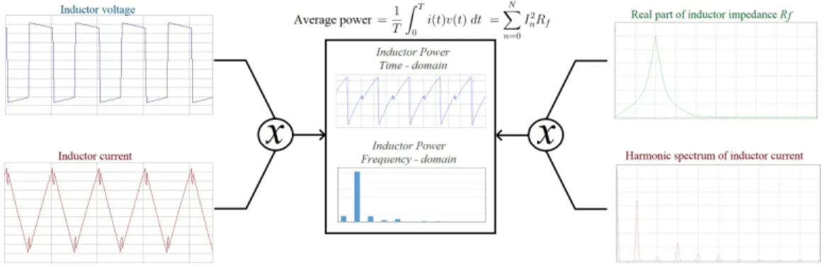
Considering the approach described in [12] and defining the inductor cur-105
rent i(t) and the inductor voltage v(t), the electrical energy ULfor an inductor
106
in the time-domain is given by eq.(1). 107 108 UL= Z ∞ −∞ p(t) dt = Z ∞ −∞ i(t)v(t) dt (1) 109 110
In the frequency-domain, the convolution theorem applied to the power 111
expression i(t)v(t) of eq.(1) is given by eq.(2), 112
113
F {i(t)v(t)} = I(f) ∗ V (f) (2) 114
115
where I(f ), V (f ) are the complex valued Fourier transforms. F denotes 116
Fourier transform, and ∗ denotes convolution. By definitions of Fourier trans-117
form F and convolution, the eq.(2) becomes eq.(3), 118 119 Z ∞ −∞ i(t)v(t) e−j2πσ dt = Z ∞ −∞ I(f )V (σ − f ) df (3) 120 121
the evaluation of the Fourier transform at the origin (σ = 0) equals the 122
integrals over all their domains [REF REF]. Thus, the electrical energy UL
123
from eq.(1) can be expressed by eq.(4), where V (f ) is the complex conju-124
gated of V (f ), 125
Z ∞ −∞ i(t)v(t) dt = Z ∞ −∞ I(f )V (f ) df (4) 127 128 therefore, 129 130 Z ∞ −∞ i(t)v(t) dt = Z ∞ −∞ I(f )[I(f )Z(f )] df = Z ∞ −∞ I(f )2Z(f ) df (5) 131 132
given that Z(f ) = Rf + jXL is the complex impedance of the inductor
133
and XL is an odd function [12],
134 135 Z ∞ −∞ i(t)v(t) dt = Z ∞ −∞ |I(f )|2(Rf − jXL) df = Z ∞ −∞ |I(f )|2Rf df (6) 136 137
the result in eq.(6) illustrates the energy conservation between the time 138
and the frequency domains. Therefore, eq.(6) can be seen as an extension 139
of the Parseval’s theorem [12]. The physical interpretation of eq.(6) is that 140
the total energy UL of the inductor can be calculated by integrating power
141
over time or by the spectral power across frequency known the current and 142
the associated losses. The Parseval’s identity define the relation between the 143
average power of a signal h(t) and their Fourier coefficients as, 144 145 1 T Z T /2 −T /2 |h(t)|2dt = ∞ X n=−∞ |Cn|2 (7) 146 147
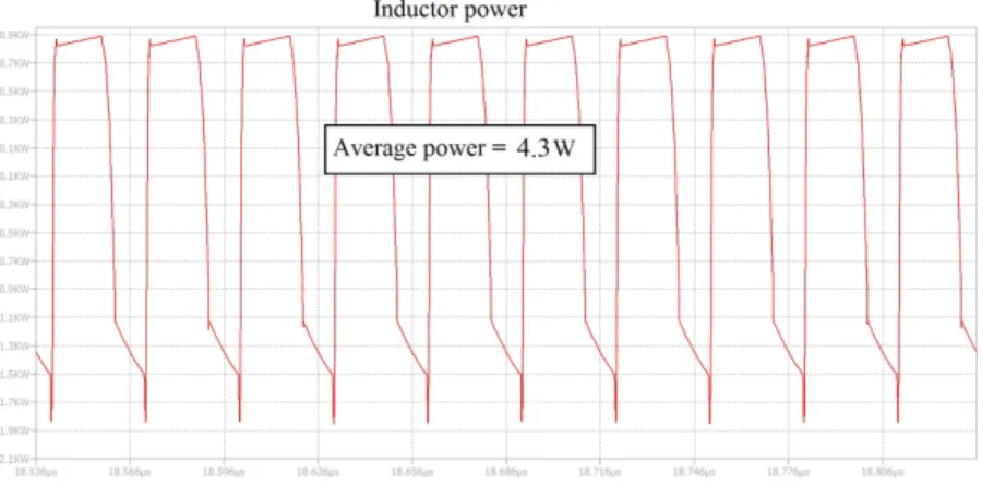
therefore, the average inductor power can be expressed from eq.(6) by, 148 149 PAV G = 1 T Z T 0 i(t)v(t) dt = N X n=0 In2Rf (8)
150 151
Figure 5: Extension of Parseval’s theorem for the inductor analysis in power converters.
As a result, the average inductor power depends on the current harmonics 152
In and the associated inductor losses Rf from the real part of the inductor
153
impedance in the frequency-domain. Fig. 5 depicts an illustrative interpre-154
tation of the developed concept about the equivalence between the power 155
in the time and the frequency domains. The right side criterion of eq.(8) is 156
applied to the designed boost converter by means of the associated inductor 157
losses Rf and the current harmonics (see Fig. 2 and Fig. 4). The results
158
for the average power in the time and frequency domains are summarizes in 159
Fig. 6 and Fig. 7. These results agree with the expected energy conservation 160
criterion. 161
162
Fig. 7 depicts the distribution of power losses in the frequency domain. 163
Results in Fig. 7 show that harmonics higher than eight times the switching 164
frequency Fsw have a negligible impact on the power losses. In addition, this
165
figure allows highlighting the contribution to the power losses of the cur-166
rent at the switching frequency. In this case, the higher losses are given at 167
the switching frequency Fsw despite of the very high ratio between the DC
168
current and the current at Fsw. The relative high value of Rf explains this
169
power losses at the switching frequency Fsw. Therefore, it is fundamental
170
to increase the quality factor Q to decrease the Rf losses at the switching
171
frequency Fsw in order to improve the global inductor efficiency.
172 173
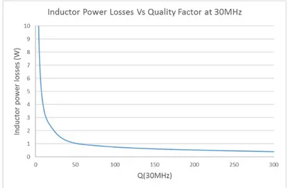
Fig. 8 shows the relation of the power losses in the time domain against 174
the quality factor at the switching frequency Q(Fsw),
Figure 6: Inductor power in the time-domain.
Figure 7: Inductor power in the frequency-domain.
176 Q(Fsw) = XL(Fsw) Rf(Fsw) (9) 177 178
The plot is calculated from eq.(8) by assuming that the highest contri-179
bution to the power losses comes from the fundamental frequency at the 180
switching frequency. To plot this figure, the SRF is assumed to be eight 181
times the switching frequency Fsw and the Q factor is evaluated at 30MHz
182
for a fixed current spectrum. Results in Fig. 8 allow concluding that increas-183
ing considerably the Q factor has low impact in the power losses since the 184
reduction in power losses becomes negligible. Therefore, it is necessary an 185
approach to the suitable selection of the Q factor. In this context, the next 186
section will propose a circuital model to include the SRF and Q parameters 187
in the converter design process to assess their impact in the converter per-188
formance and to further inductor selection or manufacturing. 189
190
Figure 8: Inductor losses and quality factor Qsw at the switching frequency Fsw.
4. Proposed inductor model including SRF and Q 191
Currently, development of power electronics requires power inductors able 192
to operate in high-frequency with high current capabilities. Therefore, the 193
manufacturing specifications of SRF and Q should be useful to both power 194
converter designers and inductor manufactures. As a result, this section pro-195
vides a framework to integrate these parameters in the design process of 196
power converters. 197
198
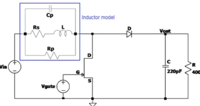
Fig. 9 describes a circuital model for actual inductors usually used for 199
the circuit simulation tools. This model includes an ideal inductor L, a series 200
resistance Rs, a parasite capacitance Cp, and a parallel losses resistance Rp.
201 202
For the inductor model of Fig. 9, the inductor impedance Z is given by 203
the eq.(10) at the switching frequency Fsw and ωsw = 2πFsw,
204 205
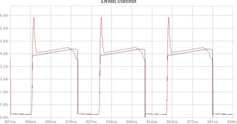
Figure 9: Boost converter with inductor model. Z = 1 1 Rp +1 − ω 2 swLCp+ jωswCpRs Rs+ jωswL (10) 206 207
considering the real and imaginary parts of Z and solving for Qsw, where
208
Qsw is defined as the quality factor at the switching frequency Q(Fsw), we
209 have, 210 211 Qsw = Im(Z) Re(Z) = −Rp(ωswCpR2s− ωswL + ω3swCpL2) R2 s+ ω2swL2+ RpRs (11) 212 213 solving for Rp, 214 215 Rp = Qsw(Rs2+ ωsw2 L2) −ω3 swCpL2+ ωswL − ωswCpR2s − QswRs (12) 216 217
Additionally, the SF R is defined by the inductor resonance frequency. 218
Thus, the Cp capacitance is given by,
219 220
Cp =
1
221 222
Eq.(12) and eq.(13) allow including in the circuital inductor model the 223
high-frequency parameters of Self Resonance Frequency (SRF ) and the qual-224
ity factor at the switching frequency Qsw. Therefore, these expressions are
225
useful to simulate and evaluate the impact of the SRF and Q parameters on 226
the power converter performance. 227
228
As illustrative example, the boost converter of Fig. 9 is simulated for 229
Fsw=30MHz, L=8.2µH, and Rs=0.2Ω. Rpand Cpare calculated from eq.(12)
230
and eq.(13). Qsw=100 in the analyzed cases. The simulation results of Fig.
231
10 show the impact on the drain current of the GaN-HEMT transistor when 232
SRF is evaluated for 30MHz and 250MHz. These results depicts the in-233
creasing in the drain current by around 50% which lead to an increase in 234
the switching losses by around 20%. This phenomenon is mainly generated 235
by the increase of the parasitic capacitance Cp when the SRF parameter is
236
lower. 237
238
Figure 10: Impact of the SRF on the drain current. Color nomenclature: blue - drain current for SRF =250MHz, red - drain current for SRF =30MHz.
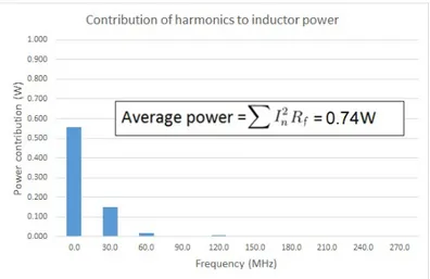
Fig. 11 depicts the frequency behavior of the associated inductor losses 239
Rf and the quality factor Qf for a power inductor of 8.2µH, Q(30MHz) = 100
240
and SRF = 250MHz. Fig. 12 shows the inductor current for the aforemen-241
tioned specifications in comparison with an ideal inductor. The frequency 242
distribution of power losses are plotted in Fig. 13. This figure shows that 243
the selected inductor drastically decreases the power losses at the switching 244
frequency. 245
246
Figure 11: Frequency behavior of Rf and Qf for the modeled inductor.
Figure 12: Inductor current. Color nomenclature: blue – ideal inductor with low series resistance, red – power inductor considering Q(30MHz) = 100 and SRF = 250MHz.
The proposed analysis for power inductors has been described through 247
this document. The simulated results have shown a suitable trade-off be-248
tween power and frequency performance. Next section will introduce the 249
experimental setup to validate the proposed approach. 250
Figure 13: Inductor power distribution in the frequency-domain for Q(30MHz)=100 and SRF = 250MHz.
5. Experimental results 251
This section describes the performed tests. First, the power inductors 252
are measured and the circuital models are validated. Then, an experimental 253
setup allows verifying the described power equivalence between the time and 254
frequency domains. Finally, an experimental boost converter provides results 255
about the performance of a conventional power inductor in a relative high-256
frequency. 257
5.1. Inductor circuital model and characterization 258
This test employs an impedance analyzer Agilent 4294A to measure the 259
parameters of several power inductors. The impedance analyzer sweeps the 260
frequency from 40Hz to 110MHz and it measures Z − θ, R − X and L − Q. 261
Table 1 summarizes the measured and calculated parameters. Rp and Cp
262
calculated from eq.(12) to eq.(13) selecting the Q factor at 10MHz in all 263
cases. Fig. 14 depicts the simulated and measured Rf (the real part of the
264
inductor impedance) for the inductor SRP5015TA. The MAPE (Mean Ab-265
solute Percentage Error) evaluates the model accuracy using eq.(14) where 266
MK is the measured value and Sk is the simulated value. As listed in Table
267
1, the MAPE shows a partial agreement between the experimental data and 268
the circuital model. 269
M AP E = 1 n n X k=1 Mk− Sk Mk (14) 271 272
However, Fig. 14 allows concluding that values for frequencies farther to 273
the selected Q at 10MHz have less agreement than values around the selected 274
Q. Therefore, the circuital model can slightly lose accuracy in a wide range 275
of frequencies. 276
277
Table 1: Characterization and modeling of inductors
Measure Calculation
Inductor Ref. L Rs Q SRF Rp Cp MAPE
(µH) (mΩ) (10MHz) (MHz) (KΩ) (pF)
SRP5015TA-8R2M 7.8 190 25.5 24.2 15.3 5.6 0.28 SRR1210-8R2Y 7.3 4.1 15.4 21.1 9.1 7.9 0.27 7447713082 7.7 29 13.2 29.8 7.2 3.7 0.28 744314850 8.2 24 7.7 35.4 4.3 2.5 0.15
5.2. Inductor power in the time-domain and the frequency-domain 278
In this experimental setup, a waveform generator (33612A Keysight) pro-279
vides a square signal of 5Vpp to the inductor under test. The current probe 280
(Tektronix CT2) measures the inductor current, and the active probe(RT-281
ZS20 R&S) measures the voltage. The oscilloscope (RTO-1044 R&S) records 282
the waveforms and calculates the average power in the time domain and the 283
inductor current FFT (Fast Fourier Transform) in the frequency domain. 284
The test is carried out at 10MHz and 30MHz. The aim of this test is to 285
validate the power equivalence using the proposed approach. 286
287
Fig. 15 depicts the waveforms for square signals of case (a) for 10MHz 288
and case (b) for 30MHz for the power inductor SRP5015A. In the case (a), 289
the fundamental frequency is lower than the SRF . Therefore, the inductor 290
is able to store energy as a magnetic field with relative low power loss. In 291
contrast, the case (b) has a fundamental frequency higher than the SRF . As 292
result, the inductor behaves as a capacitor distorting the current signal and 293
increasing the power loss. 294
295
Fig. 16 shows the FFT for the inductor current of case (a) in Fig. 15a. 296
In Table 2, the contribution of each harmonic is calculated from the mea-297
sured Rf (see Fig. 14) and the FFT (see Fig. 16) for the fundamental and
298
harmonic frequencies using expression eq.(15). Results from Fig. 15a and 299
Table 2 agree with the expected correlation between the power in the time 300
and frequency domains. 301 302 PAV G = 1 T Z T 0 i(t)v(t) dt = N X n=0 In2Rf (15) 303 304
Table 2: Inductor power frequency-domain (SRP5015A). Test at 10MHz - square signal.
Freq.(MHz) 0 10 30 50 70 90 Total Ph(µW) 0.03 197 14 4.8 2.9 1.7 220
(a) Test at 10MHz. Pavg = 239µW.
Time-scale: 40ns/div
(b) Test at 30MHz. Pavg = 848µW.
Time-scale: 10ns/div Figure 15: Test inductor SRP5015A at 10MHz and 30MHz.
Figure 16: FFT of inductor current for test at 10MHz - square signal. Inductor reference SRP5015A.
Table 3 summaries the power results for the measured inductors. These 305
results confirm the duality between the inductor power in the time-domain 306
and the frequency-domain. However, differences between theoretical and 307
experimental results are mainly caused by the shifting of the SRF given the 308
parasitic capacitance and inductance of the current and voltage probes. 309
5.3. Boost converter at 1MHz 310
This test implements a boost converter at 1MHz. The boost converter 311
specification are Vin=30V, Vout=60V, Pout=40W, and inductor current IL=1.5A
Table 3: Inductor power in the time and frequency SRP5015TA-8R2M SRR1210-8R2Y 10MHz 30MHz 10MHz 30MHz Power time (µW) 239 848 257 925 Power freq.(µW) 220 760 235 857 7447713082 744314850 10MHz 30MHz 10MHz 30MHz Power time (µW) 285 1380 299 818 Power freq.(µW) 262 1140 283 767
considering an efficiency η=0.9. The design uses and inductor SRR1210-8R2 313
given its favorable quality factor Q(1MHz)=30 and SRF =22MHz. The se-314
lected inductor SRR1210-8R2 has a series resistance Rs=17mΩ and a
sat-315
uration current of 7.5A. The switching frequency is set to 1MHz to ensure 316
the eight harmonic lower than the SRF . A GaN-HEMT is used as a switch-317
ing device. The achieved results harmonize with the theoretical framework. 318
However, the slight deviation between the temporal and frequency responses 319
can be overcame by improving the experimental setup decreasing the para-320
sitic elements. 321
322
Figure 17: Experimental results for 1MHz boost converter. Inductor SRR1210-8R2. Pavg=492mW.
Fig. 17 shows the inductor waveforms. The inductor average power in the 323
time-domain is Pavg=492mW. Fig. 18 depicts the harmonic spectrum for the
324
inductor current. Table 4 lists the power contribution of each harmonic to 325
the total power. The total power in the frequency-domain is Pavg=447mW.
326
Results from Fig. 17 and Table 4 validate the equivalence between the power 327
in the time and frequency domains. In additions, the results allow identifying 328
that the behavior at the fundamental frequency is the main cause of the 329
inductor power loss. 330
Figure 18: FFT for the inductor current of 1MHz boost converter.
Table 4: Inductor power in the frequency domain
Freq.(MHz) 0 1 2 3 4 5 Total Ph(mW) 14 418 0.4 11 0.05 2.7 447
5.4. Boost converter for 400V - 400W at 30MHz 331
This section shows the results of implementing a high-frequency boost 332
converter. A power inductor was designed for this experimental setup. The 333
designed inductor has specifications of L=8µH, Isat=3.5A, Q(30M Hz)=25
334
and SRF =200MHz. The switching device is a GaN-HEMT. 335
336
The boost converter is tested first at Vout=60V - Pout=10W and after at
337
Vout=400V - Pout=400W. The test is carried out first in relative low power
338
to use available current probe (Tektronix CT2) because current probes for 339
high-current, high-voltage and high-frequency are currently under develop-340
ment. This represents a research challenge. In the second case, the inductor 341
current is not measure for previous reasons. However, the global power con-342
verter results shows the suitable performance of the designed inductor. 343
344
In the first test, the specifications of the boost converter are Vin=30V,
345
Vout=60V, and Pout=10W at 30MHz. Fig. 19 shows the waveforms for the
346
power inductor. In this case, the average power was Pavg=780mW in the
347
time-domain and Pavg=700mW in the frequency-domain.
348
(a) Inductor current test at 60V - 30MHz (b) Inductor current and voltage Figure 19: Inductor current and voltage for boost converter 60V - 10W at 30MHz
Figure 20: Experimental setup boost converter 400V - 400W at 30MHz.
For the second test, the implemented high-frequency boost converter has 349
specifications of Vin=200V, Vout=400V, Pout=400W at 30MHz. Fig. 20 shows
350
the experimental setup for the high-frequency boost converter. Additionally, 351
result of Fig. 21 depicts the behavior of the output voltage. As shown in Fig. 352
21, the designed boost converter is able to increase the input voltage from 353
200V to 400V with an output load of 400W. The switching frequency is set to 354
30MHz to assess the GaN-HEMT devices at high-voltage and high-frequency 355
given a suitable performance. As a consequence, these results confirm the 356
pertinence of the developed modeling approach to analyze and design power 357
inductors to take advantages of the switching characteristics of GaN-HEMT 358
devices. 359
360
Figure 21: Output voltage of boost converter 400V - 400W at 30MHz.
6. Conclusions 361
The reported methodology has associated the analysis in the time and 362
frequency domains for inductors in power converters using an extension of 363
the Parseval’s theorem. The proposed approach is complementary to con-364
ventional methodologies for the design of power converters. This analysis 365
methodology allowed determining suitable criteria for the selection and sim-366
ulation of inductors according to expected power losses. The proposed ap-367
proach allowed disaggregating the power losses in the frequency-domain for 368
complex inductor power signals in the time-domain. The study of the quality 369
factor Q allowed concluding that increasing considerably Q has low impact 370
on the power losses since the reduction in power losses becomes negligible. 371
Therefore, a moderate Q factor can be selected to achieve a trade-off between 372
inductor performance and manufacturing feasibility. Additionally, the Self 373
Resonance Frequency SRF around eight times the switching frequency is a 374
suitable criterion to avoid inductor current distortion. The proposed model 375
in this work included frequency parameters of inductors in the design process 376
of power converters. The experimental results have validated the proposed 377
approach. However, the experimental setup should decrease the parasitic 378
inductance and capacitance to minimize the measurement disturbances at 379
high-frequency. 380
Acknowledgments 381
This work has been partially funded by the Region Occitanie Pyrenees-382
Mediterranee. 383
References 384
[1] P. Ning, T. Yuan, Y. Kang, C. Han, and L. Li, “Review of si igbt 385
and sic mosfet based on hybrid switch,” Chinese Journal of Electrical 386
Engineering, vol. 5, pp. 20–29, Sep. 2019. 387
[2] J. Kashiwagi, A. Yamaguchi, Y. Moriyama, and K. Nakahara, “Hys-388
teretic control embedded boost converter operating at 25-mhz switch-389
ing,” IEEE Transactions on Circuits and Systems II: Express Briefs, 390
vol. 66, pp. 101–105, Jan 2019. 391
[3] A. Hariya, K. Matsuura, H. Yanagi, S. Tomioka, Y. Ishizuka, and T. Ni-392
nomiya, “Five-megahertz pwm-controlled current-mode resonant dc–dc 393
step-down converter using gan-hemts,” IEEE Transactions on Industry 394
Applications, vol. 51, pp. 3263–3272, July 2015. 395
[4] M. Rodr´ıguez, Y. Zhang, and D. Maksimovic, “High-frequency pwm 396
buck converters using gan-on-sic hemts,” IEEE Transactions on Power 397
Electronics, vol. 29, pp. 2462–2473, May 2014. 398
[5] A. Hilal and B. Cougo, “Optimal inductor design and material selec-399
tion for high power density inverters used in aircraft applications,” in 400
2016 International Conference on Electrical Systems for Aircraft, Rail-401
way, Ship Propulsion and Road Vehicles International Transportation 402
Electrification Conference (ESARS-ITEC), pp. 1–6, Nov 2016. 403
[6] W. Liang, L. Raymond, and J. Rivas, “3-d-printed air-core inductors for 404
high-frequency power converters,” IEEE Transactions on Power Elec-405
tronics, vol. 31, pp. 52–64, Jan 2016. 406
[7] A. F. Jaimes, F. L. Cabrera, and F. R. de Sousa, “Characterization of 407
high- q inductors up to its self-resonance frequency for wireless power 408
transfer applications,” IEEE Microwave and Wireless Components Let-409
ters, vol. 28, pp. 1071–1073, Dec 2018. 410
[8] D. C. Corrˆea, U. C. Resende, and F. S. Bicalho, “Experiments with 411
a compact wireless power transfer system using strongly coupled mag-412
netic resonance and metamaterials,” IEEE Transactions on Magnetics, 413
vol. 55, pp. 1–4, Aug 2019. 414
[9] Kaiwei Yao, Yang Qiu, Ming Xu, and F. C. Lee, “A novel winding-415
coupled buck converter for high-frequency, high-step-down dc-dc conver-416
sion,” IEEE Transactions on Power Electronics, vol. 20, pp. 1017–1024, 417
Sep. 2005. 418
[10] E. L. Barrios, A. Urtasun, A. Urs´ua, L. Marroyo, and P. Sanchis, “Op-419
timal dc gapped inductor design including high-frequency effects,” in 420
IECON 2015 - 41st Annual Conference of the IEEE Industrial Elec-421
tronics Society, pp. 003928–003933, Nov 2015. 422
[11] R. Barrera-Cardenas, T. Isobe, and M. Molinas, “Optimal design of air-423
core inductor for medium/high power dc-dc converters,” in 2016 IEEE 424
17th Workshop on Control and Modeling for Power Electronics (COM-425
PEL), pp. 1–8, June 2016. 426
[12] S. S. Kelkar, L. L. Grigsby, and J. Langsner, “An extension of parseval’s 427
theorem and its use in calculating transient energy in the frequency do-428
main,” IEEE Transactions on Industrial Electronics, vol. IE-30, pp. 42– 429
45, Feb 1983. 430